Computational Investigation of the Folded and Unfolded Band Structure and Structural and Optical Properties of CsPb(I1−xBrx)3 Perovskites

 ,
,  , and
, and
Abstract
:1. Introduction
2. Computational Method
3. Results and Discussions
3.1. Structural Properties
3.2. Electronic Properties
3.3. Density of States
3.4. Optical Properties
4. Conclusions
Supplementary Materials
Author Contributions
Funding
Acknowledgments
Conflicts of Interest
References
- Mao, X.; Sun, L.; Wu, T.; Chu, T.; Deng, W.; Han, K. First-Principles Screening of All-Inorganic Lead-Free ABX3 Perovskites. J. Phys. Chem. C 2018, 122, 7670–7675. [Google Scholar] [CrossRef]
- Im, J.H.; Lee, C.R.; Lee, J.W.; Park, S.W.; Park, N.G. 6.5% Efficient Perovskite Quantum-Dot-Sensitized Solar Cell. Nanoscale 2011, 3, 4088–4093. [Google Scholar] [CrossRef] [Green Version]
- Gao, P.; Gratzel, M.; Nazeeruddin, M.K.; Online, V.A.; Gao, P.; Nazeeruddin, M.K. Environmental Science Organohalide lead perovskites for photovoltaic applications. Energy Environ. Sci. 2014, 7, 2448–2463. [Google Scholar] [CrossRef]
- Correa-Baena, J.P.; Abate, A.; Saliba, M.; Tress, W.; Jesper Jacobsson, T.; Grätzel, M.; Hagfeldt, A. The rapid evolution of highly efficient perovskite solar cells. Energy Environ. Sci. 2017, 10, 710–727. [Google Scholar] [CrossRef]
- Zhao, Y.; Zhu, K. Organic-inorganic hybrid lead halide perovskites for optoelectronic and electronic applications. Chem. Soc. Rev. 2016, 45, 655–689. [Google Scholar] [CrossRef] [PubMed]
- Sum, T.C.; Mathews, N. Advancements in perovskite solar cells: Photophysics behind the photovoltaics. Energy Environ. Sci. 2014, 7, 2518–2534. [Google Scholar] [CrossRef] [Green Version]
- Eidsvåg, H.; Rasukkannu, M.; Vajeeston, P.; Velauthapillai, D. Bandgap engineering in CsSnxPb(1−x)I3 and their influence on light absorption. Mater. Lett. 2018, 218, 253–256. [Google Scholar] [CrossRef]
- Maqbool, M.; Rehman, G.; Ali, L.; Shafiq, M.; Iqbal, R.; Ahmad, R.; Khan, T.; Jalali-Asadabadi, S.; Maqbool, M.; Ahmad, I. Structural, electronic and optical properties of CsPbX3 (X = Cl, Br, I) for energy storage and hybrid solar cell applications. J. Alloys Compd. 2017, 705, 828–839. [Google Scholar]
- Afsari, M.; Boochani, A.; Hantezadeh, M. Electronic, optical and elastic properties of cubic perovskite CsPbI3: Using first principles study. Optik (Stuttg). 2016, 127, 11433–11443. [Google Scholar] [CrossRef]
- Jishi, R.A.; Ta, O.B.; Sharif, A.A. Modeling of lead halide perovskites for photovoltaic applications. J. Phys. Chem. C 2014, 118, 28344–28349. [Google Scholar] [CrossRef] [Green Version]
- Ilyas, B.M.; Elias, B.H. A theoretical study of perovskite CsXCl3 (X = Pb, Cd) within first principles calculations. Phys. B Condens. Matter 2017, 510, 60–73. [Google Scholar] [CrossRef]
- Moore, D.T.; Kamino, B.A.; Patel, J.B.; Miranda, L.; Johnston, M.B.; Parrott, E.S.; Haghighirad, A.A.; Hörantner, M.T.; Sutton, R.J.; Snaith, H.J.; et al. Bandgap-Tunable Cesium Lead Halide Perovskites with High Thermal Stability for Efficient Solar Cells. Adv. Energy Mater. 2016, 6, 1502458. [Google Scholar]
- Duan, J.; He, B.; Li, Y.; Tang, Q.; Zhao, Y.; Yuan, H. Lattice Modulation of Alkali Metal Cations Doped Cs1−xRxPbBr3 Halides for Inorganic Perovskite Solar Cells. Sol. RRL 2018, 2, 1800164. [Google Scholar]
- Chen, X.; Han, D.; Su, Y.; Zeng, Q.; Liu, L.; Shen, D. Structural and Electronic Properties of Inorganic Mixed Halide Perovskites. Phys. Status Solidi Rapid Res. Lett. 2018, 12, 1800193. [Google Scholar] [CrossRef]
- Shi, J.; Yun, S. First-Principles DFT Calculations for Perovskite Solar Cells. In Counter Electrodes for Dye—Sensitized and Perovskite Solar Cells, II; Yun, S., Hagfeldt, A., Eds.; Wiley-VCH Verlag GmbH & Co. KGaA: Weinheim, Germany, 2018; pp. 487–509. [Google Scholar]
- Umari, P.; Mosconi, E.; De Angelis, F. Relativistic GW calculations on CH3NH3PbI3 and CH3NH3SnI3 Perovskites for Solar Cell Applications. Sci. Rep. 2014, 4, 4467. [Google Scholar] [CrossRef] [Green Version]
- Li, B.; Zhang, Y.; Fu, L.; Yu, T.; Zhou, S.; Zhang, L.; Yin, L. Surface passivation engineering strategy to fully-inorganic cubic CsPbI3 perovskites for high-performance solar cells. Nat. Commun. 2018, 9, 1076. [Google Scholar] [CrossRef]
- Wang, P.; Zhang, X.; Zhou, Y.; Jiang, Q.; Ye, Q.; Chu, Z.; Li, X.; Yang, X.; Yin, Z.; You, J. Solvent-controlled growth of inorganic perovskite films in dry environment for efficient and stable solar cells. Nat. Commun. 2018, 9, 2225. [Google Scholar] [CrossRef]
- Liu, C.; Hu, M.; Zhou, X.; Wu, J.; Zhang, L.; Kong, W.; Li, X.; Zhao, X.; Dai, S.; Xu, B.; et al. Efficiency and stability enhancement of perovskite solar cells by introducing CsPbI3 quantum dots as an interface engineering layer. NPG Asia Mater. 2018, 10, 552–561. [Google Scholar] [CrossRef]
- Wang, K.; Jin, Z.; Liang, L.; Bian, H.; Bai, D.; Wang, H.; Zhang, J.; Wang, Q.; Liu, S. All-inorganic cesium lead iodide perovskite solar cells with stabilized efficiency beyond 15%. Nat. Commun. 2018, 9, 4544. [Google Scholar] [CrossRef] [Green Version]
- Chen, M.; Ju, M.G.; Garces, H.F.; Carl, A.D.; Ono, L.K.; Hawash, Z.; Zhang, Y.; Shen, T.; Qi, Y.; Grimm, R.L.; et al. Highly stable and efficient all-inorganic lead-free perovskite solar cells with native-oxide passivation. Nat. Commun. 2019, 10, 16. [Google Scholar] [CrossRef] [Green Version]
- Kohn, W.; SHAM, L.J. Self-Consistent Equations Including Exchange and Correlation Effects. Phys. Rev. 1965, 140, A1133. [Google Scholar] [CrossRef] [Green Version]
- Perdew, J.P.; Burke, K.; Ernzerhof, M. Generalized gradient approximation made simple. Phys. Rev. Lett. 1996, 77, 3865–3868. [Google Scholar] [CrossRef] [PubMed] [Green Version]
- Tran, F.; Blaha, P. Accurate band gaps of semiconductors and insulators with a semilocal exchange-correlation potential. Phys. Rev. Lett. 2009, 102, 226401. [Google Scholar] [CrossRef] [PubMed] [Green Version]
- Bylander, D.M.; Kleinman, L. Good semiconductor band gaps with a modified local-density approximation. Phys. Rev. B 1990, 41, 7868–7871. [Google Scholar] [CrossRef]
- Bechstedt, F.; Fuchs, F.; Kresse, G. Ab-initio theory of semiconductor band structures: New developments and progress. Phys. Status Solidi Basic Res. 2009, 246, 1877–1892. [Google Scholar] [CrossRef]
- Camargo-Martínez, J.A.; Baquero, R. The band gap problem: The accuracy of the wien2k code confronted. Rev. Mex. Fis. 2013, 59, 453–459. [Google Scholar]
- Heyd, J.; Peralta, J.E.; Scuseria, G.E.; Martin, R.L. Energy band gaps and lattice parameters evaluated with the Heyd-Scuseria-Ernzerhof screened hybrid functional. J. Chem. Phys. 2005, 123, 174101. [Google Scholar] [CrossRef]
- Koller, D.; Tran, F.; Blaha, P. Improving the modified Becke-Johnson exchange potential. Phys. Rev. B Condens. Matter Mater. Phys. 2012, 85, 155109. [Google Scholar] [CrossRef] [Green Version]
- Perdew, J.P.; Zunger, A. Self-interaction correction to density-functional approximations for many-electron systems. Phys. Rev. B 1981, 23, 5048–5079. [Google Scholar] [CrossRef] [Green Version]
- Yuan, Y.; Xu, R.; Xu, H.T.; Hong, F.; Xu, F.; Wang, L.J. Nature of the band gap of halide perovskites ABX3(A = CH3NH3, Cs; B = Sn, Pb; X = Cl, Br, I): First-principles calculations. Chinese Phys. B 2015, 24, 116302. [Google Scholar] [CrossRef]
- Ray, D.; Clark, C.; Pham, H.Q.; Borycz, J.; Holmes, R.J.; Aydil, E.S.; Gagliardi, L. Computational Study of Structural and Electronic Properties of Lead-Free CsMI3 Perovskites (M = Ge, Sn, Pb, Mg, Ca, Sr, and Ba). J. Phys. Chem. C 2018, 122, 7838–7848. [Google Scholar] [CrossRef]
- He, M.; Ding, L.; Liu, S.; Shao, G.; Zhang, Z.; Liang, X.; Xiang, W. Superior fluorescence and high stability of B-Si-Zn glasses based on Mn-doped CsPbBrxI3−x nanocrystals. J. Alloys Compd. 2019, 780, 318–325. [Google Scholar] [CrossRef]
- Eperon, G.E.; Stranks, S.D.; Menelaou, C.; Johnston, M.B.; Herz, L.M.; Snaith, H.J. Formamidinium lead trihalide: A broadly tunable perovskite for efficient planar heterojunction solar cells. Energy Environ. Sci. 2014, 7, 982–988. [Google Scholar] [CrossRef]
- Castelli, I.E.; García-Lastra, J.M.; Thygesen, K.S.; Jacobsen, K.W. Bandgap calculations and trends of organometal halide perovskites. APL Mater. 2014, 2, 081514. [Google Scholar] [CrossRef] [Green Version]
- Goesten, M.G.; Hoffmann, R. Mirrors of Bonding in Metal Halide Perovskites. J. Am. Chem. Soc. 2018, 140, 12996–13010. [Google Scholar] [CrossRef] [PubMed]
- Kang, B.; Biswas, K. Exploring Polaronic, Excitonic Structures and Luminescence in Cs4PbBr6/CsPbBr3. J. Phys. Chem. Lett. 2018, 9, 830–836. [Google Scholar] [CrossRef] [PubMed]
- Wolf, C.; Lee, T.W. Exciton and lattice dynamics in low-temperature processable CsPbBr3 thin-films. Mater. Today Energy 2018, 7, 199–207. [Google Scholar] [CrossRef]
- Zhang, M.; Zheng, Z.; Fu, Q.; Chen, Z.; He, J.; Zhang, S.; Chen, C.; Luo, W. Synthesis and single crystal growth of perovskite semiconductor CsPbBr3. J. Cryst. Growth 2018, 484, 37–42. [Google Scholar] [CrossRef]
- Stoumpos, C.C.; Malliakas, C.D.; Peters, J.A.; Liu, Z.; Sebastian, M.; Im, J.; Chasapis, T.C.; Wibowo, A.C.; Chung, D.Y.; Freeman, A.J.; et al. Crystal growth of the perovskite semiconductor CsPbBr3: A new material for high-energy radiation detection. Cryst. Growth Des. 2013, 13, 2722–2727. [Google Scholar] [CrossRef]
- Yaffe, O.; Guo, Y.; Tan, L.Z.; Egger, D.A.; Hull, T.; Stoumpos, C.C.; Zheng, F.; Heinz, T.F.; Kronik, L.; Kanatzidis, M.G.; et al. The nature of dynamic disorder in lead halide perovskite crystals. In Physical Chemistry of Interfaces and Nanomaterials XV, SPIE Nanoscience + Engineering, 28 August–1 September 2016; Bakulin, A.A., Lovrincic, R., Banerji, N., Eds.; SPIE: San Diego, CA, USA, 2016; Volume 9923, p. 99231B. [Google Scholar]
- Akkerman, Q.A.; Motti, S.G.; Srimath Kandada, A.R.; Mosconi, E.; D’Innocenzo, V.; Bertoni, G.; Marras, S.; Kamino, B.A.; Miranda, L.; De Angelis, F.; et al. Solution Synthesis Approach to Colloidal Cesium Lead Halide Perovskite Nanoplatelets with Monolayer-Level Thickness Control. J. Am. Chem. Soc. 2016, 138, 1010–1016. [Google Scholar] [CrossRef] [PubMed] [Green Version]
- Paul, T.; Chatterjee, B.K.; Maiti, S.; Sarkar, S.; Besra, N.; Das, B.K.; Panigrahi, K.J.; Thakur, S.; Ghorai, U.K.; Chattopadhyay, K.K. Tunable cathodoluminescence over the entire visible window from all-inorganic perovskite CsPbX3 1D architecture. J. Mater. Chem. C 2018, 6, 3322–3333. [Google Scholar] [CrossRef]
- Liu, Z.; Peters, J.A.; Stoumpos, C.C.; Sebastian, M.; Wessels, B.W.; Im, J.; Freeman, A.J.; Kanatzidis, M.G. Heavy metal ternary halides for room-temperature X-ray and gamma-ray detection. In Hard X-ray Gamma-ray Neutron Detect. Phys. XV, Proceedings of SPIE—The International Society for Optical Engineering, 25–29 August 2013; Fiederle, M., Burger, A., Franks, L., James, R.B., Eds.; SPIE: San Diego, CA, USA, 2013; Volume 8852, p. 88520A. [Google Scholar]
- Koller, D.; Tran, F.; Blaha, P. Merits and limits of the modified Becke-Johnson exchange potential. Phys. Rev. B 2011, 83, 195134. [Google Scholar] [CrossRef] [Green Version]
- Rubel, O.; Bokhanchuk, A.; Ahmed, S.J.; Assmann, E. Unfolding the band structure of disordered solids: From bound states to high-mobility Kane fermions. Phys. Rev. B Condens. Matter Mater. Phys. 2014, 90, 115202. [Google Scholar] [CrossRef] [Green Version]
- Maspero, R.; Sweeney, S.J.; Florescu, M. Unfolding the band structure of GaAsBi. J. Phys. Condens. Matter 2017, 29, 075001. [Google Scholar] [CrossRef]
- Medeiros, P.V.C.; Stafström, S.; Björk, J. Effects of extrinsic and intrinsic perturbations on the electronic structure of graphene: Retaining an effective primitive cell band structure by band unfolding. Phys. Rev. B Condens. Matter Mater. Phys. 2014, 89, 041407. [Google Scholar] [CrossRef] [Green Version]
- Hohenberg, P.; Kohn, W. Inhomogeneous Electron Gas. Phys. Rev. 1964, 134, B864. [Google Scholar] [CrossRef] [Green Version]
- Nordström, L.; Madsen, G.K.H.; Blaha, P.; Schwarz, K.; Sjöstedt, E. Efficient linearization of the augmented plane-wave method. Phys. Rev. B Condens. Matter Mater. Phys. 2001, 64, 195134. [Google Scholar]
- Blaha, P.; Schwarz, K.; Luitz, G.K.H.M.D.K.J.; Tran, R.L.F.; Marks, L.D. An Augmented Plane Wave Plus Local Orbitals Program for Calculating Crystal Properties, 3rd-9501031st-ed.; Schwarz, K., Ed.; Vienna University of Technology: Vienna, Austria, 2019; Volume 2, ISBN 3-9501031-1-2. [Google Scholar]
- Momma, K.; Izumi, F. VESTA 3 for three-dimensional visualization of crystal, volumetric and morphology data. J. Appl. Crystallogr. 2011, 44, 1272–1276. [Google Scholar] [CrossRef]
- Ghaithan, H.M.; Alahmed, Z.A.; Qaid, S.M.H.; Aldwayyan, A.S. First principle-based calculations of the optoelectronic features of 2 × 2 × 2 CsPb(I1−xBrx)3 perovskite. Superlattices Microstruct. 2020, 140, 106474. [Google Scholar] [CrossRef]
- Trots, D.M.; Myagkota, S.V. High-temperature structural evolution of caesium and rubidium triiodoplumbates. J. Phys. Chem. Solids 2008, 69, 2520–2526. [Google Scholar] [CrossRef] [Green Version]
- Eperon, G.E.; Paternò, G.M.; Sutton, R.J.; Zampetti, A.; Haghighirad, A.A.; Cacialli, F.; Snaith, H.J. Inorganic caesium lead iodide perovskite solar cells. J. Mater. Chem. A 2015, 3, 19688–19695. [Google Scholar] [CrossRef]
- Ghaithan, H.M.; Alahmed, Z.A.; Qaid, S.M.H.; Hezam, M.; Aldwayyan, A.S. Density Functional Study of Cubic, Tetragonal, and Orthorhombic CsPbBr3 Perovskite. ACS Omega 2020, 5, 7468–7480. [Google Scholar] [CrossRef] [PubMed] [Green Version]
- Murtaza, G.; Ahmad, I. First principle study of the structural and optoelectronic properties of cubic perovskites CsPbM3 (M = Cl, Br, I). Phys. B Condens. Matter 2011, 406, 3222–3229. [Google Scholar] [CrossRef]
- Sandor, E.; Wooster, W.A. Crystal Structure and Photoconductivity of Cæsium Plumbohalides. Nature 1958, 182, 1436. [Google Scholar]
- Dixit, H.; Saniz, R.; Cottenier, S.; Lamoen, D.; Partoens, B. Electronic structure of transparent oxides with the Tran-Blaha modified Becke-Johnson potential. J. Phys. Condens. Matter 2012, 24, 205503. [Google Scholar] [CrossRef]
- Fan, S.W.; Ding, L.J.; Yao, K.L. Electronic structure and ferromagnetism of boron doped bulk and surface CdSe: By generalized gradient approximation and generalized gradient approximation plus modified Becke and Johnson calculations. J. Appl. Phys. 2013, 114, 113905. [Google Scholar] [CrossRef]
- Traoré, B.; Bouder, G.; Lafargue-Dit-Hauret, W.; Rocquefelte, X.; Katan, C.; Tran, F.; Kepenekian, M. Efficient and accurate calculation of band gaps of halide perovskites with the Tran-Blaha modified Becke-Johnson potential. Phys. Rev. B 2019, 99, 035139. [Google Scholar] [CrossRef] [Green Version]
- Popescu, V.; Zunger, A. Effective band structure of random alloys. Phys. Rev. Lett. 2010, 104, 236403. [Google Scholar] [CrossRef]
- Popescu, V.; Zunger, A. Extracting E versus Effective band structure from supercell calculations on alloys and impurities. Phys. Rev. B Condens. Matter Mater. Phys. 2012, 85, 085201. [Google Scholar] [CrossRef] [Green Version]
- Chen, M.X.; Weinert, M. Revealing the substrate origin of the linear dispersion of Silicene/Ag(111). Nano Lett. 2014, 14, 5189–5193. [Google Scholar] [CrossRef] [PubMed] [Green Version]
- Lang, L.; Yang, J.H.; Liu, H.R.; Xiang, H.J.; Gong, X.G. First-principles study on the electronic and optical properties of cubic ABX3 halide perovskites. Phys. Lett. A 2014, 378, 290–293. [Google Scholar] [CrossRef] [Green Version]
- Heidrich, K.; Schäfer, W.; Schreiber, M.; Söchtig, J.; Trendel, G.; Treusch, J.; Grandke, T.; Stolz, H.J. Electronic structure, photoemission spectra, and vacuum-ultraviolet optical spectra of CsPbCl3 and CsPbBr3. Phys. Rev. B 1981, 24, 5642–5649. [Google Scholar] [CrossRef]
- Wang, K.; Yang, Q.; Duan, J.; Zhang, C.; Zhao, F.; Yu, H.; Hu, B. Spin-Polarized Electronic Transport through Ferromagnet/Organic–Inorganic Hybrid Perovskite Spinterfaces at Room Temperature. Adv. Mater. Interfaces 2019, 1, 1900718. [Google Scholar] [CrossRef]
- Qaid, S.M.H.; Al-Asbahi, B.A.; Ghaithan, H.M.; AlSalhi, M.S.; Al dwayyan, A.S. Optical and structural properties of CsPbBr3 perovskite quantum dots/PFO polymer composite thin films. J. Colloid Interface Sci. 2020, 563, 426–434. [Google Scholar] [CrossRef]
- Ghebouli, M.A.; Ghebouli, B.; Fatmi, M. First-principles calculations on structural, elastic, electronic, optical and thermal properties of CsPbCl3 perovskite. Phys. B Condens. Matter 2011, 406, 1837–1843. [Google Scholar] [CrossRef]
- Amin, B.; Ahmad, I.; Maqbool, M.; Goumri-Said, S.; Ahmad, R. Ab initio study of the bandgap engineering of Al1−xGaxN for optoelectronic applications. J. Appl. Phys. 2011, 109, 023109. [Google Scholar] [CrossRef] [Green Version]
- Xu, B.; Li, X.; Sun, J.; Yi, L. Electronic structure, ferroelectricity and optical properties of CaBi2Ta2O9. Eur. Phys. J. B 2008, 66, 483–487. [Google Scholar] [CrossRef]


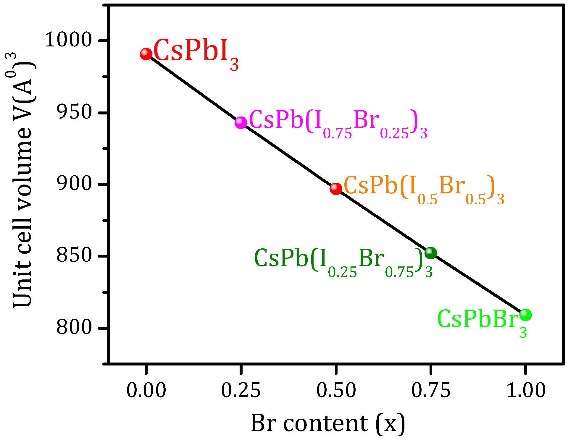
| CsPb(I1−xBrx)3 | Lattice Constants (Å) | Unit-Cell Volume V(Å)3 | B (GPa) | B’ | ||
|---|---|---|---|---|---|---|
| This Study | Previous Studies (Exp.) | This Study | This Study | Previous Studies | This Study | |
| CsPbI3 | 6.28 | 6.40 [9] (PBE-GGA) 6.4004 [53] (PBE-GGA) 6.14 [9] (LDA) 6.25 [9] (PBEsol-GGA) 6.39 [14] (PBE-GGA) (6.29) [54] (6.18) [55] | 990.69 | 14.5770 | 14.3971 [9] (PBE-GGA) 20.220 [9] (LDA) 16.910 [9] (PBEsol-GGA) | 4.502 |
| CsPb(I0.75Br0.25)3 | 6.1775 | 6.395 [14] (PBE-GGA) | 942.97 | -- | -- | -- |
| CsPb(I0.5Br0.5)3 | 6.075 | 5.990 [14] (PBE-GGA) | 896.81 | -- | -- | -- |
| CsPb(I0.25Br0.75)3 | 5.9725 | 5.997 [14] (PBE-GGA) | 852.17 | -- | -- | -- |
| CsPbBr3 | 5.87 | 6.0051 [8] (PBE-GGA) 6.00549 [53] (PBE-GGA) 6.009 [31] (PBE-GGA) 5.875 [56] (PBEsol-GGA) 6.046 [31] (HSE) 5.999 [14] (PBE-GGA) 5.84 [57] (WC-GGA) (5.874) [58] | 809.05 | 18.7612 | -- | 4.2192 |
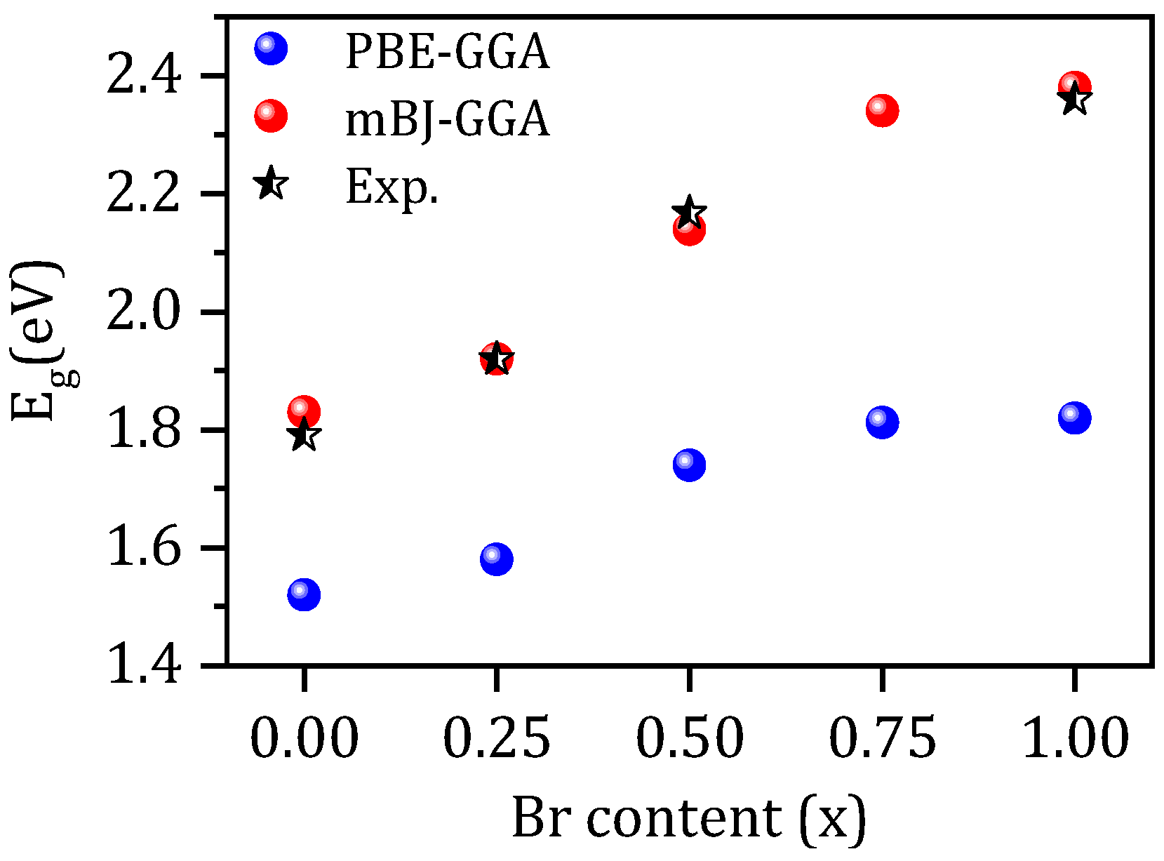
| CsPb(I1−xBrx)3 x = | Eg(eV) | |||
|---|---|---|---|---|
| This Study | Other Calculations | |||
| PBE-GGA | mBJ-GGA | Theoretical | Experimental | |
| 0.00 | 1.52 | 1.83 | 1.485 [32] (PBE-GGA) 1.938 [32] (HSE06) 1.359 [31] (PBE-GGA) 1.56 [9] (PBE-GGA) 1.879 [9] (mBJ-GGA) 1.478 [8] (PBE-GGA) 1.75 [8] (nTmBJ) 1.90 [53] (PBE-GGA) | 1.791 [33] 1.73 [34] |
| 0.25 | 1.58 | 1.92 | -- | 1.92 [12] |
| 0.50 | 1.74 | 2.14 | -- | 2.167 [33] |
| 0.75 | 1.81 | 2.34 | -- | -- |
| 1.00 | 1.82 | 2.38 | 1.60 [57] (WC-GGA) 2.41 [65] (HSE) 1.482 [14] (PBE-GGA) 1.764 [31] (PBE-GGA) 2.50 [53] (PBE-GGA) | 2.30 [66] 2.36 [67] 2.32 [13] 2.282 [68] |
© 2020 by the authors. Licensee MDPI, Basel, Switzerland. This article is an open access article distributed under the terms and conditions of the Creative Commons Attribution (CC BY) license (http://creativecommons.org/licenses/by/4.0/).
Share and Cite
Ghaithan, H.M.; Alahmed, Z.A.; Lyras, A.; Qaid, S.M.H.; Aldwayyan, A.S. Computational Investigation of the Folded and Unfolded Band Structure and Structural and Optical Properties of CsPb(I1−xBrx)3 Perovskites. Crystals 2020, 10, 342. https://0-doi-org.brum.beds.ac.uk/10.3390/cryst10050342
Ghaithan HM, Alahmed ZA, Lyras A, Qaid SMH, Aldwayyan AS. Computational Investigation of the Folded and Unfolded Band Structure and Structural and Optical Properties of CsPb(I1−xBrx)3 Perovskites. Crystals. 2020; 10(5):342. https://0-doi-org.brum.beds.ac.uk/10.3390/cryst10050342
Chicago/Turabian StyleGhaithan, Hamid M., Zeyad A. Alahmed, Andreas Lyras, Saif M. H. Qaid, and Abdullah S. Aldwayyan. 2020. "Computational Investigation of the Folded and Unfolded Band Structure and Structural and Optical Properties of CsPb(I1−xBrx)3 Perovskites" Crystals 10, no. 5: 342. https://0-doi-org.brum.beds.ac.uk/10.3390/cryst10050342