Article

Polarization Splitter-Rotator Based on Multimode Waveguide Grating

1
Laboratory of Biomedical Photonics & Engineering, Life Science Institute, Guangxi Medical University, Nanning 530021, China
2
State Key Laboratory of Optoelectronic Materials and Technologies, School of Electronics and Information Technology, Sun Yat-Sen University, Guangzhou 510275, China
3
Laboratory of Biomedical Photonics & Engineering, School of Basic Medical Sciences, Guangxi Medical University, Nanning 530021, China
4
Department of Physics, East Carolina University, Greenville, NC 27858-4353, USA
5
School of Economics and Commerce, South China University of Technology, Guangzhou 510640, China
6
Longgang Center for Disease Control and Prevention, Shenzhen 518172, China
*
Author to whom correspondence should be addressed.
Submission received: 7 September 2021 / Revised: 20 September 2021 / Accepted: 24 September 2021 / Published: 26 September 2021
(This article belongs to the Special Issue Photonic Crystals and Their Applications)

Abstract

:
We demonstrate a polarization splitter rotator (PSR) based on multimode waveguide grating (MWG) on a silicon-on-insulator (SOI) platform. Bloch mode hybridization in mini-stopband is exploited to achieve high polarization conversion efficiency. The fabricated device yields a high extinction ratio of > 53 dB and > 31 dB, low crosstalk of < −26.4 dB and < −40 dB for the injected TE0 and TM0 mode, with average insertion loss of 1.2 dB and 1.5 dB in the wavelength regime 1552 nm–1562 nm. Such a device shows great design flexibility and an easy fabrication process, serving as a good candidate in integrated polarization diversity circuits, especially for applications requiring spectra manipulation. Additionally, the polarization conversion approach provides opportunities to develop novel polarization management devices.

1. Introduction

Silicon-on-insulator (SOI) has become one of the most promising platforms for photonic integration benefiting from its low cost, high-density integration, and compatibility with CMOS fabrication processes. However, the high index contrast introduces significant polarization dependence, which makes silicon photonic devices incompatible with fiber communication applications where the polarization state in optical fiber is typically random. One efficient solution to eliminate the polarization sensitivity is to use a polarization splitter-rotator (PSR) [1,2,3,4,5], in which the TE0 mode and TM0 mode can be separated into two individual waveguides. Meanwhile, one of the polarization states will be converted to the orthogonal one, normally chosen as TE0 mode considering that most devices are optimized only for TE0 polarization. Such a polarization handling device is also desired on other material platforms, and has been demonstrated on platforms including InP [6,7], SiN [8] and lithium-niobate-on-insulator (LNOI) [9,10]. Vertical asymmetrical structures are normally required to implement polarization conversion schemes including covering different cladding material [1], fabricating a bi-level taper [11,12], or introducing additional top structures such as gold [13] and SiN [14]. The operation principle of PSRs can be classified into two categories of mode coupling [15] and mode evolution [16,17], according to the energy exchange path when polarization rotation. For mode coupling based PSRs, phase-matching condition should be satisfied. The typical structures adopted are asymmetrical directional coupler (ADC) [18], tapered DC [19], bend DC [20,21], and so on. For mode evolution ones, mode hybridization between TM0 mode and forward TE1 mode can occur when light propagates along the adiabatic taper or multimode waveguide [22]. It should be noted that all the reported PSRs are designed for broadband operation, aiming as universal schemes for realizing polarization-transparent photonic integrated circuits (PICs). However, for some critical applications such as polarization insensitive wavelength division (de)multiplexer [23,24], wavelength selective devices such as arrayed waveguide gratings (AWGs) are subsequently required to implement wavelength multiplexing [25], inevitably incurring extra insertion loss and footprint and design complexity to the whole on-chip system. Exploiting novel polarization conversion mechanisms and developing new functional devices are desirable for PICs application.
Mini-stopband (MSB) is derived from the anti-crossing between Bloch modes [26,27]. There have been numerous interesting applications based on MSB, mostly in two dimensional photonic crystal (2D-PhC) such as pulse compression [28], coarse wavelength selection [29], optical filters [30], and selective mirroring in PhC lasers [31,32]. Several functional components based on MSB have also been demonstrated including polarization beam splitter [33] and tunable optical band stop filters [34], in one dimensional photonic crystal (1D-PhC). However, the authors have never considered in particular the coupling between Bloch modes with different polarization, and resultant polarization conversion in multimode waveguide grating (MWG).
In this paper, we demonstrate a novel MWG-based PSR. An anti-crossing of Bloch modes in MSB is exploited to archive highly efficient polarization rotation. The proposed PSR boasts a high extinction ratio, low crosstalk, an easy fabrication process, and great design flexibility. Additionally, such a device can be further cascaded with grating assisted contra-directional couplers (contra-DCs) [35,36], paving the way for critical applications such as polarization insensitive wavelength division (de)multiplexer [23,24] and multichannel polarization-multiplexed differential quadrature phase-shift keying (PM-DQPSK) transceiver [37,38].

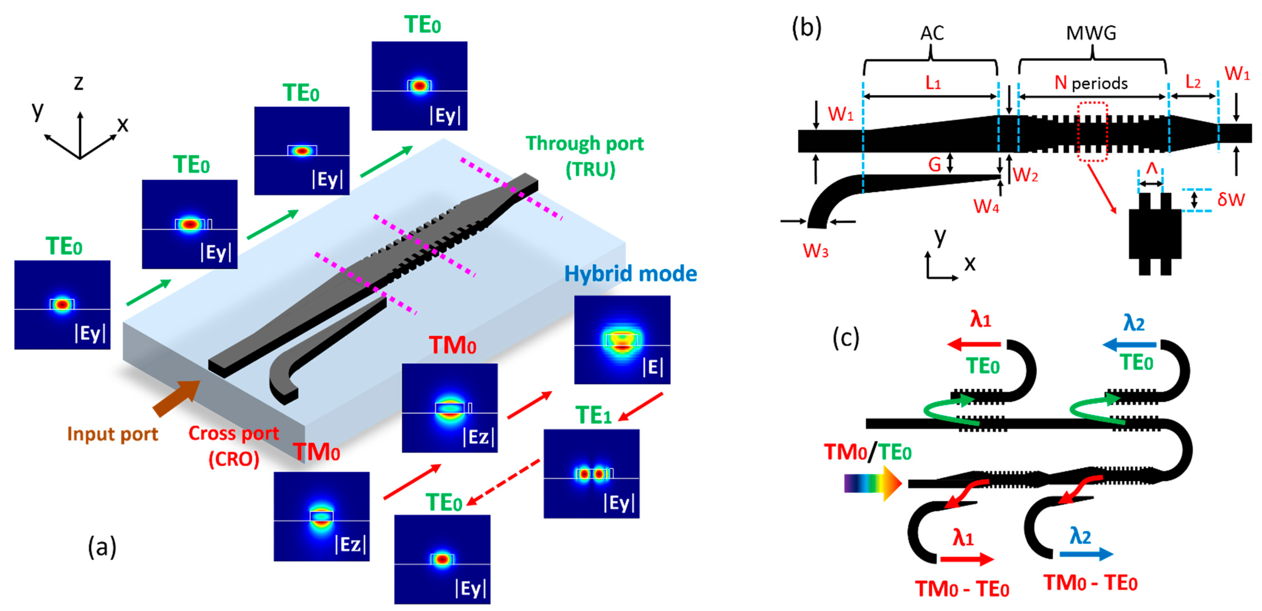
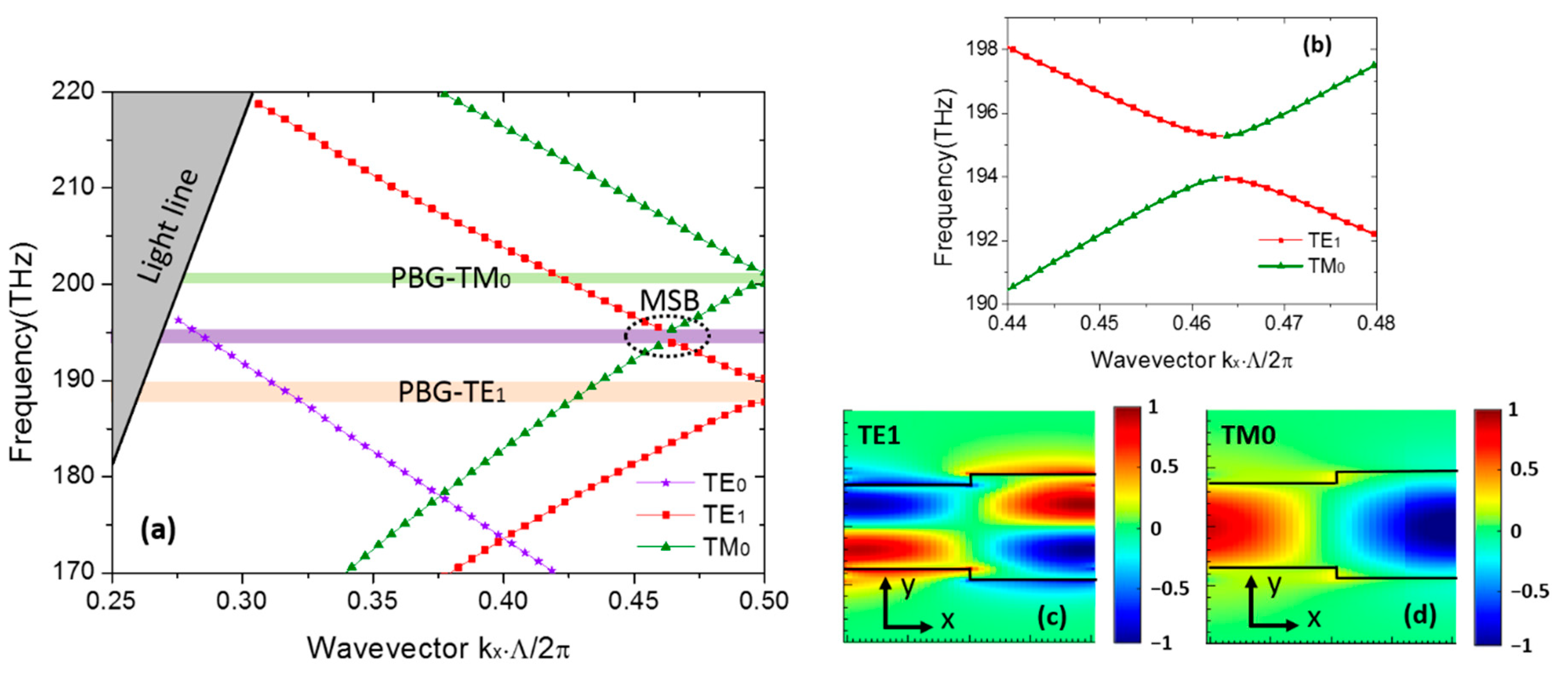
2. Device Structure and Working Principle

The proposed PSR is schematically illustrated in Figure 1, and consists of a linearly tapered multimode waveguide grating (MWG) and adiabatic coupler (AC). The silicon strip waveguides are 220 nm high sitting on a 2 μm buried oxide layer with air cladding, for the demand of vertical symmetry breaking. For the injected TE0 mode, the light beam keeps propagating along AC, MWG, and linearly tapered waveguide (length L2), then exits at the through (TRU) port. In the case of TM0 input, the mode is first preserved in the AC region (length L1, Gap G), then reversely coupled to be the TE1 mode by MWG due to the satisfied phase-matching condition and Bloch mode hybridization. In the AC section, the backward TE1 mode finally evolves into a TE0 mode of the isolated bottom taper waveguide (width from W4 to W3) and bends away to the cross (CRO) port.
The structure parameters of width, period, grating number, and corrugation width in the uniform MWG region are denoted by W2, ᴧ, N, and δw, respectively, as labeled in Figure 1b. As a potential application scenario, we also propose an easy architecture of a polarization insensitive wavelength duplexer, simply by cascading MWG-based PSR and grating assisted contra-directional coupler. As depicted in Figure 1c, the injected TM0 mode will be backward converted to TE0 by PSR and dropped at different ports because of the different grating period ᴧ. Meanwhile, the injected TE0 mode propagates through the whole PSRs region, is then dropped to different ports by contra-DCs. Note that the longitudinal-apodization design is normally requires suppressing the sidelobe of the spectra and reducing channel crosstalk.
To illustrate the working principle of the proposed PSR, we calculated the photonic band structure of uniform MWG using the three-dimensional finite-difference time-domain (3D-FDTD) method, with structure parameters: = 414 nm, W2 = 900 nm, δw = 100 nm, fill factor ff = 0.5. For the unit cell, non-uniform meshing is utilized with minimum mesh sizes Δxmin = Δymin = 10 nm, and Δzmin = 20 nm. Bloch periodic boundary conditions are imposed on the two surfaces perpendicular to the x-axis, and perfectly matched layer (PML) boundary conditions are applied on the other surfaces. Figure 2a shows the band structure of TE0, TE1, and TM0 Bloch mode. The photonic band gaps (PBGs) are located at 187.8 THz–190.2 THz, 200.07 THz–201.2 THz, respectively, which means that there is no allowed mode in uniform MWG. Anti-crossing between TM0 and TE1 modes can also be observed, giving rise to a MSB at frequencies ranging from 194.0 THz to 195.3 THz (or wavelengths from 1.536 μm to 1.547 μm). Hence, the input TM0 mode located in MSB can be converted to backward TE1 Bloch mode, and vice-versa. Note that the conversion between the TM0 and TE1 Bloch modes in the uniform MWG should satisfy the phase matching condition: λc/ᴧ = (Neff1 + Neff2), where Neff1 and Neff2 represent the effective refractive indices of the two coupled Bloch modes, and λc is central wavelength. The group indices NgTE1 and NgTM0 of both modes can be extracted from the slope of their dispersion relation, taken far from the coupling region [27]. The value of coupling coefficient κ can be derived by the following expression [39]:
κ = π N g Δ λ / λ c 2
where Δ λ is bandwidth of MSB, and N g = ( N g T E 0 + N g T M 1 ) / 2 . For the uniform MWG considered above, the parameters extracted from the dispersion diagram of Figure 2a are NgTE1 = 5.05, NgTM0 = 4.11, and Δ λ / λ c 2 = 0.463 × 10 3 m 1 , leading to κ = 6.66 × 10 3 m 1 . This value is lower than the one of common waveguide Bragg gratings without polarization conversion, typically > 50 × 10 3 m 1 [40]. Additionally, we can effectively tune κ by using lateral phase delay modulation [41], for the purpose of apodization design. Figure 2b shows the local picture of MSB associated to the coupling between TM0 and TE1 Bloch modes. The electric field patterns are represented in Figure 2c,d.
Figure 3a shows the transmission and reflection spectra of uniform MWG with N = 100 when TE0 and TM0 mode are injected. The results are calculated using uniform meshing with Δxmin = Δymin = Δzmin = 20 nm, which ensure accuracy and calculation efficiency. One MSB ranging from 1.541 μm to 1.551 μm is observed; the reflection of the TM0 mode is about 96%. We note that the transmission of input TE0 mode is near 96% in MSB, while the major component of backward fields is TM1 mode. However, this crosstalk is negligible due to the weak reflection and large propagation loss of TM1 mode for the proposed device.
We further simulate light propagation profiles in uniform MWG using 3D-FDTD, at typical wavelengths of 1.546 μm, 1.509 μm, and 1.496 μm, which are presented in Figure 3b–f. As predicted in the band structure, the launched TE0 mode can maintain its polarization and propagate through uniform MWG (Figure 3b), at a wavelength of 1.546 μm. Meanwhile, the TE0 mode will be gradually attenuated as a radiation mode being located above the light line (Figure 3c), at a wavelength of 1.509 μm (198.8 THz), with a transmission of 83%. For the launched TM0 mode at 1.546 μm, the major component of backward field is TE1 mode, as shown in Figure 3d. TM0 mode is gradually attenuated at a wavelength of 1.496 μm due to being located in the PBG (Figure 3f), while freely propagating at a wavelength of 1.509 μm as a purely Bragg-guided mode (Figure 3e).
To reduce insertion loss and suppress back-reflection incurred by mode mismatch between strip waveguide and uniform MWG, two linearly tapered gratings are utilized at both ends of the uniform MWG with minimum sidewall corrugation δwmin, minimum period min, and grating number N , as seen in Figure 4a. The TM0 –TE1 conversion efficiency is equal to the fraction of power reflected into TE1 mode, which can be extracted utilizing the Mode Expansion Monitor. The transmission and reflection as a function of min are shown in Figure 4b. We can see that there is a linear variation region (340 nm < min < 390 nm) for TE0 mode, and a local minimum reflection of −46 dB for TM0 mode when min = 380 nm, which corresponds to the highest TM0 –TE1 conversion efficiency. This means that we need to make a trade-off between the transmission of TE0 mode and the reflection of TM0 mode. Here, the optimal ᴧmin is determined to be 380 nm, which guarantees an acceptable transmission of 94.2% for TE0 mode and the lowest reflection of TM0 mode, and the highest conversion efficiency of TM0 –TE1. In the following simulation, linearly tapered gratings with δwmin = 10 nm, ᴧmin = 380 nm and N = 20 are adopted.
We investigate the influence of grating number N on spectra, keeping ᴧ = 0.414 μm, W2 = 0.9 μm, δw = 0.1 μm, and ff = 50%, as shown in Figure 5a. It is seen that as N increases, the stopband edge becomes much steeper, and the maximum reflection increases significantly. Figure 5b presents the conversion efficiency and transmission as a function of grating number. As seen, the transmission of TE0 mode is higher than 92% (−0.36 dB) when N = 200, and the conversion efficiency of TM0 –TE1 is improved by up to 98% (−0.22 dB). The transmission of TM0 mode is about −46.9 dB at 1.546 μm, which could be even lower by increasing the grating number.
Next, we change the grating period ᴧ while keeping W2 = 0.9 μm, δw = 0.1 μm and N = 200. The reflection spectra shown in Figure 6a indicates that stopband is red-shifted significantly as ᴧ increases. Slight ripple (lower than 1%) in stopband caused by mode mismatch is observed. Figure 6b presents the dependence of central wavelength λc and 1-dB bandwidth on grating period quantitatively. As seen, when ᴧ increases from 0.414 μm to 0.432 μm, λc increases linearly from 1.545 μm to 1.573 μm with slope d λ c d = 1.5, and the bandwidth increases monotonously from 13 nm to 15 nm. Therefore, one can design operation wavelength of PSR by tuning grating period.
The effect of corrugation width δw on reflection spectra is investigated when W2 = 0.9 μm, ᴧ = 0.414 μm, and N = 200. As shown in Figure 7a, the stopband is red-shifted significantly as δw decreases, due to a variation of the effective refractive index in MWG. The reflection of central wavelength is diminished from 0.98 to 0.8 because of the decreasing grating strength. Figure 7b presents the dependence of central wavelength λ c and 1-dB bandwidth of the stopband on the δw quantitatively. As seen, when δw increases from 50 nm to 112.5 nm, λ c decreases with δw linearly from 1.578 μm to 1.535 μm with a slope d λ c d δ w = −0.693, and the 1-dB bandwidth increases monotonously from 6 nm to 14 nm. This indicates that the MWG-based PSR is intrinsically characterized by a narrow operation bandwidth, due to the wavelength dependence of the grating.

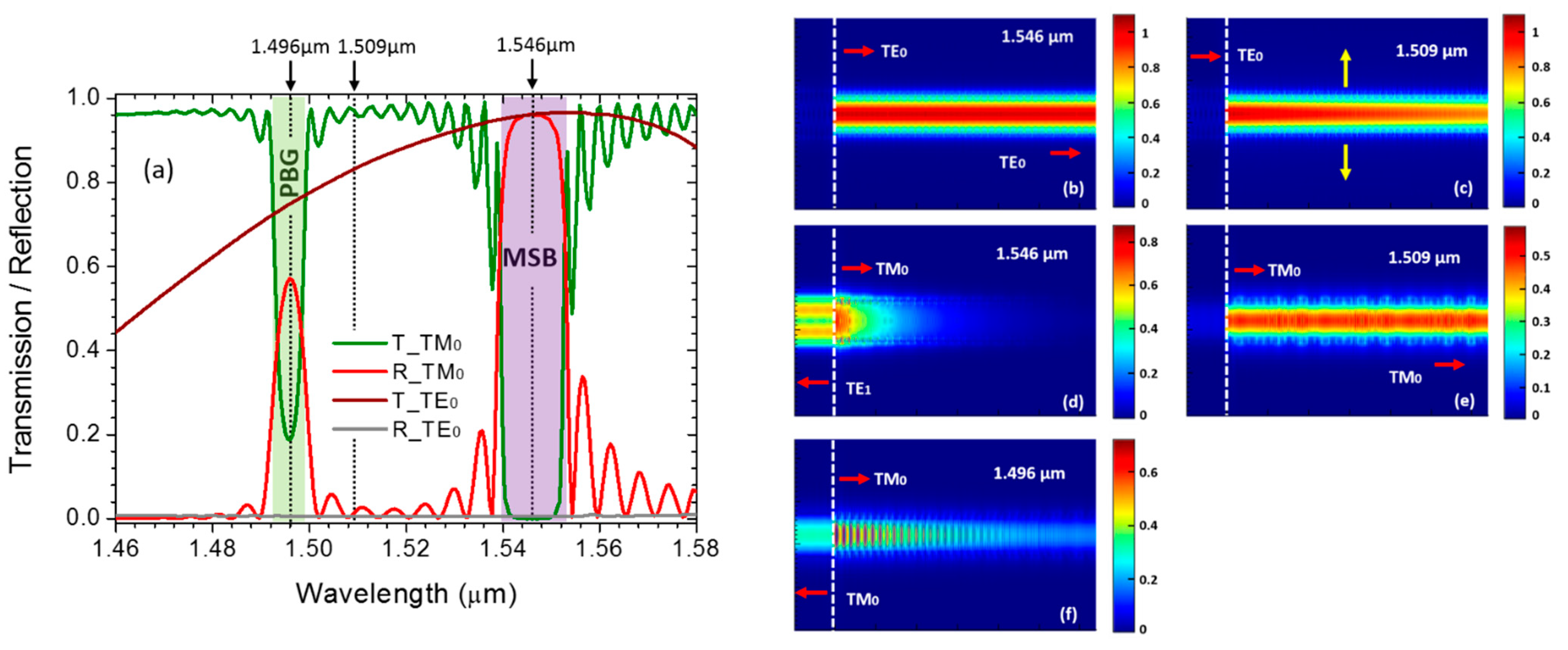
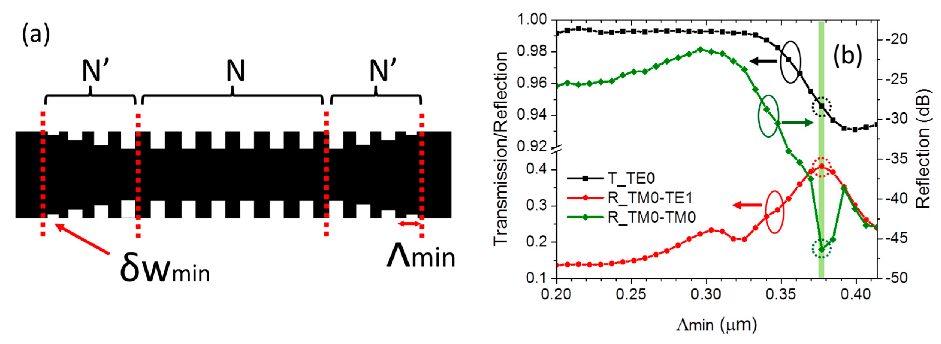
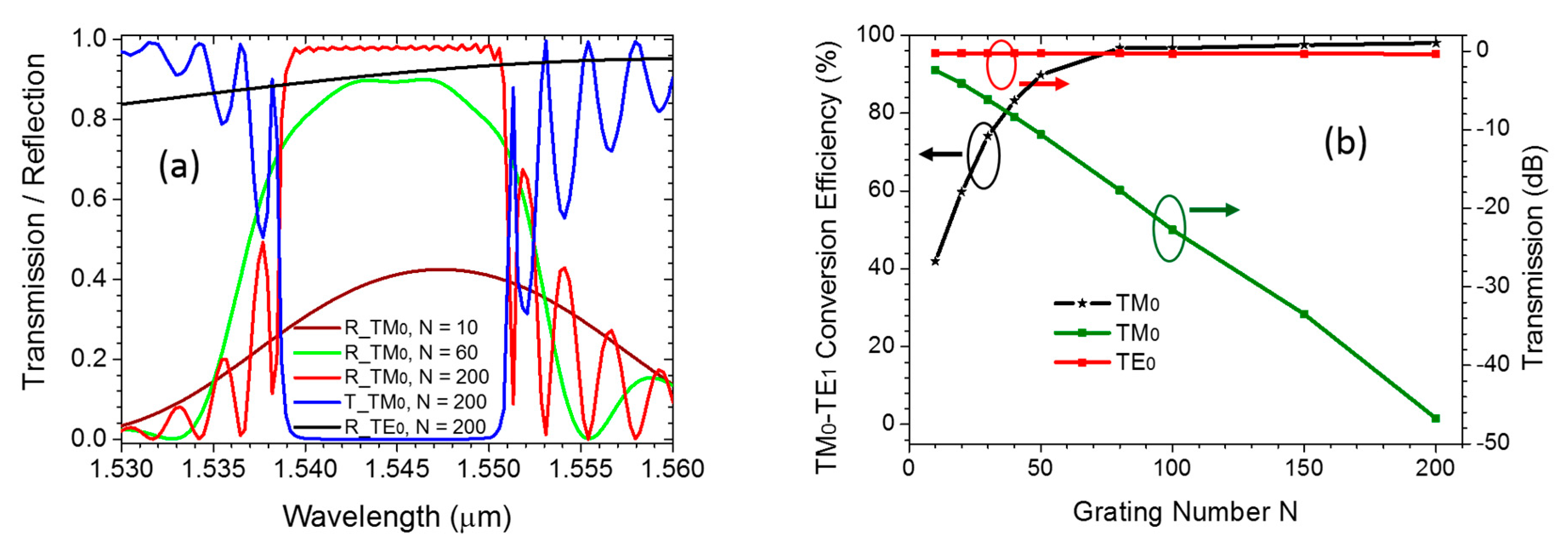
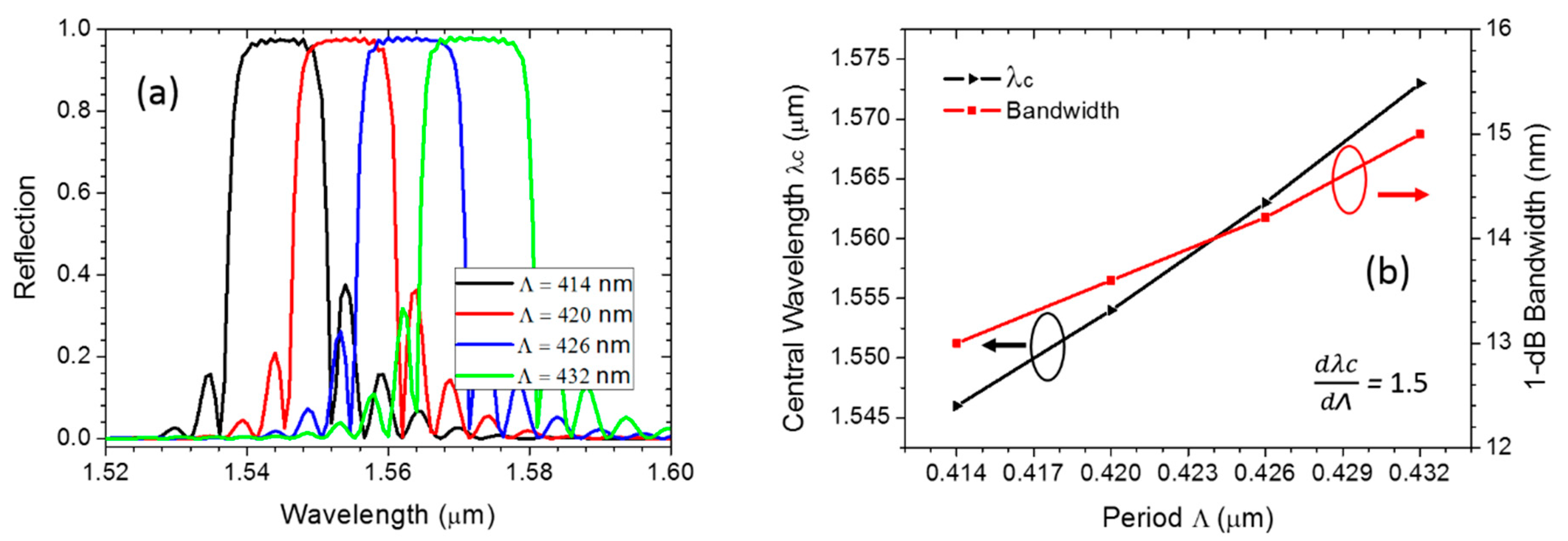
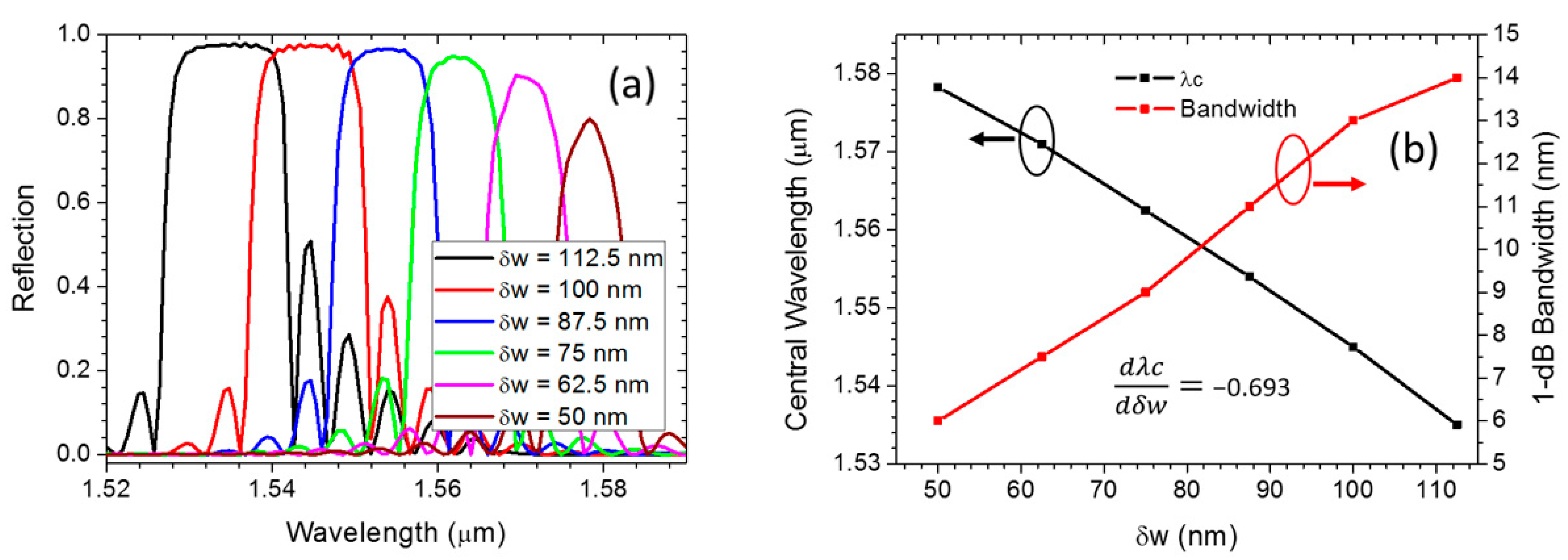
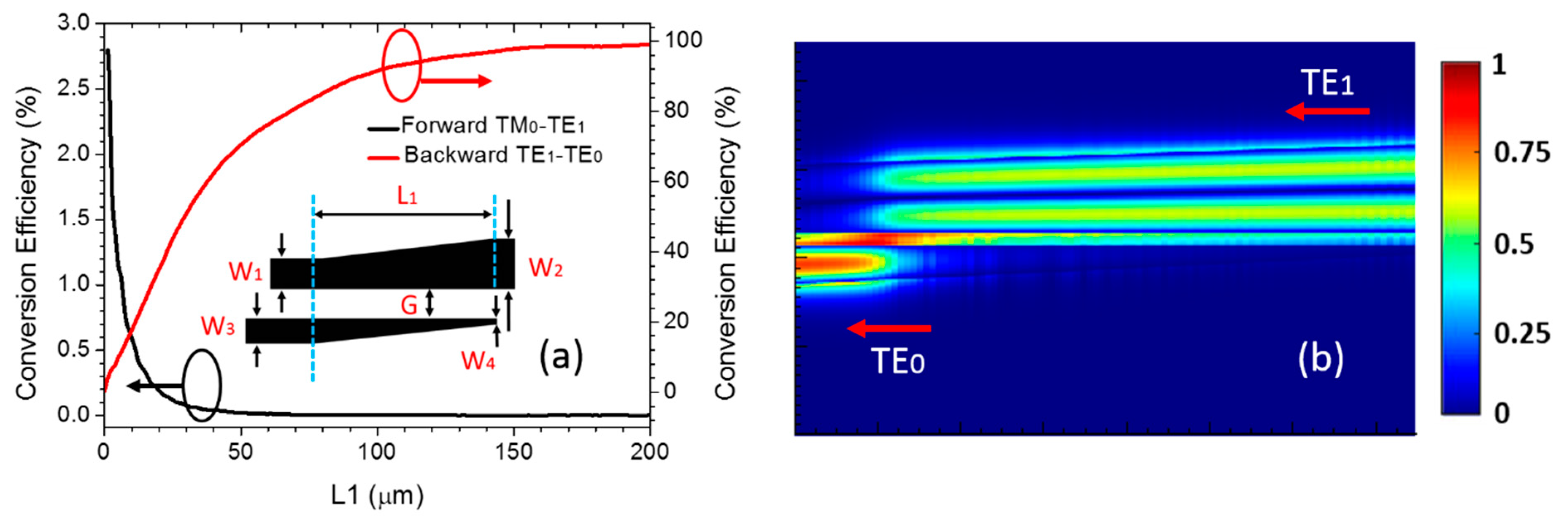
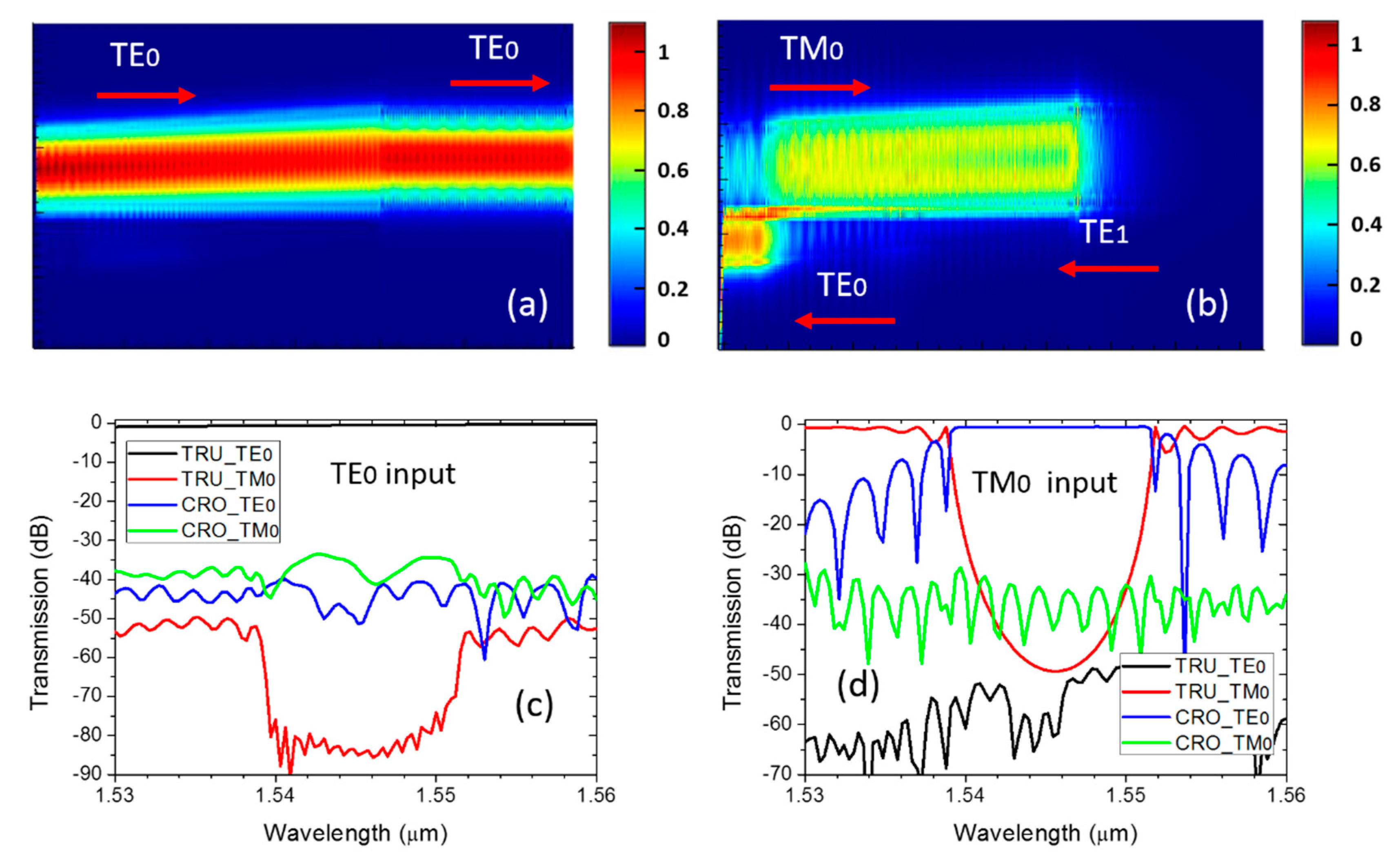
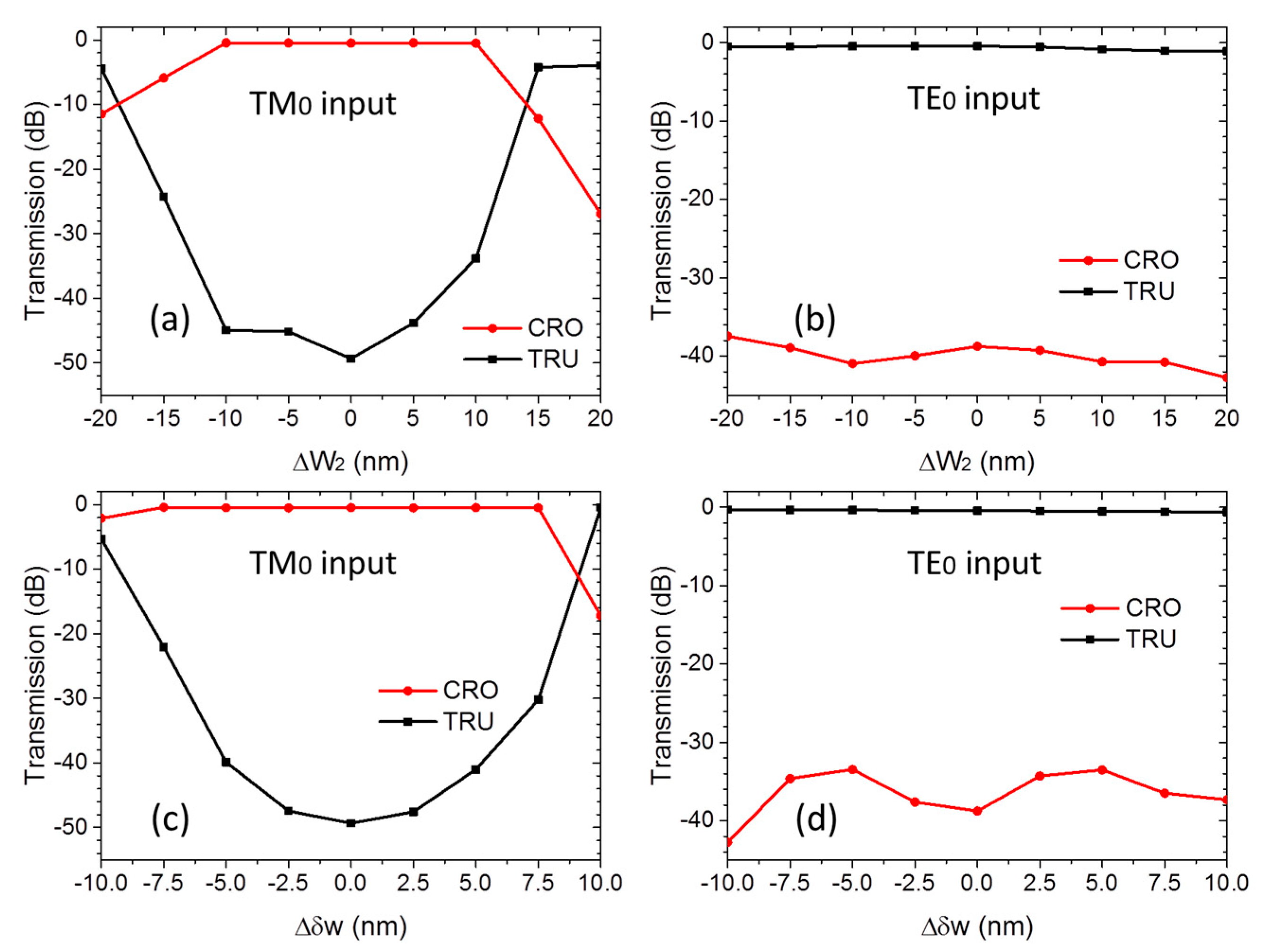
3. Device Performance and Analysis

An adiabatic coupler is adopted for the conversion between backward TE1 mode and TE0 mode because of its high conversion efficiency and large fabrication tolerance. The design parameters of AC and linear taper are optimized by the Eigenmode expansion (EME) method, which are listed as follows: W1 = 0.7 μm, W2 = 0.9 μm, W3 = 0.4 μm, W4 = 0.1 μm, G = 0.12 μm, L1 = 160 μm, L2 = 3 μm. The TE1 to TE0 conversion efficiency is up to 98.5% when L1 = 160 μm at wavelength of 1.546 μm, as shown in Figure 8. Meanwhile, the mode conversion efficiency between the forward TM0 mode and TE1 mode decreases significantly, owing to the taper width (from W1 to W2), which is far away from the mode hybridization region, about 660 nm for the case of air cladding [22].
The light propagation profiles and transmission spectra of the whole PSR are simulated using structure parameters as following: W1 = 0.7 μm, W2 = 0.9 μm, W3 = 0.4 μm, W4 = 0.1 μm, L1 = 160 μm, L2 = 3.0 μm, G = 0.12 μm, N = 200, δw = 0.1 μm, ᴧ = 0.414 μm, ff = 0.5, δwmin = 10 nm, ᴧmin = 380 nm and N = 20. As shown in Figure 9a,b, the injected TE0 mode propagates through the whole structure and outputs at the TRU port. Meanwhile, the injected TM0 mode is first reversely converted to be TE1 mode in the MWG section, then coupled to be TE0 mode in the narrow waveguide of AC section, and finally output at the CRO port. The proposed PSR is evaluated by the performance metrics of insertion loss (IL), extinction ratio (ER), and crosstalk (CT), respectively [42]. The IL, ER, and CT for input TE0 mode are defined as:
IL TE = 10 · log 10 ( T TE tru )
ER TE = 10 · log 10 ( T TM tru / T TE tru )
CT TE = 10 · log 10 ( T TE cro / T TE tru )
The IL, ER and CT for input TM0 mode are defined as:
IL TM = 10 · log 10 ( T TE cro )
ER TM = 10 · log 10 ( T TM cro / T TE cro )
CT TM = 10 · log 10 ( T TE tru / T TE cro )
where T mode port means the transmission of mode at TRU port or CRO port. The calculated transmission spectra are shown in Figure 9c,d; we note that the IL TE and IL TM are both less than 0.5 dB over 10 nm bandwidth (1.54 μm–1.55 μm). The ER TE is > 50 dB and CT TE is < −39 dB for the TE0 mode in the wavelength range of 1.53 μm–1.56 μm. Note that CT TE is theoretically originated from the backward TM1 mode excited by MWG. However, this impact is negligible for a fabricated device considering the large propagation loss of TM1 mode, which is further confirmed by our experimental results. For the input TM0 mode, ER TM of > 30 dB and CT TM of −48 dB can be observed, ranging from 1541 nm to 1550 nm. The ER TM is originated from the weakly reflected TM0 mode.
We further investigate the fabrication tolerance of the proposed PSR, assuming there is a width variation of W2 and corrugation δw. As shown in Figure 10a, when TM0 mode is launched, the PSR exhibits a performance of < 0.5 dB IL and > 30 dB CT, when ΔW2 changes from −10 nm to 10 nm. The reason can be explained by the fact that the effective refractive index in MWG is sensitive to the width variation; therefore, the phase-match condition and stopband are affected. However, the transmission of TE0 mode (Figure 10b) is only slightly affected by ΔW2; the CT is > 36 dB, and IL is < 0.6 dB, showing a robust performance. The device performance affected by the corrugation width δw is shown in Figure 10c,d. For the TM0 mode, a high CT of > 20 dB is obtained, when Δδw varies from −7.5 nm to 7.5 nm, assuming W2 = 0.9 μm. However, this influence is slight for TE0 mode (Figure 10d). Overall, the proposed PSR exhibits different performance according to the structure variations, for TE0 mode and TM0 mode, respectively. Additionally, for the injected TM0 mode, the influence of Δδw is more significant than ΔW2. The proposed device can be fabricated by advanced fabrication technologies.

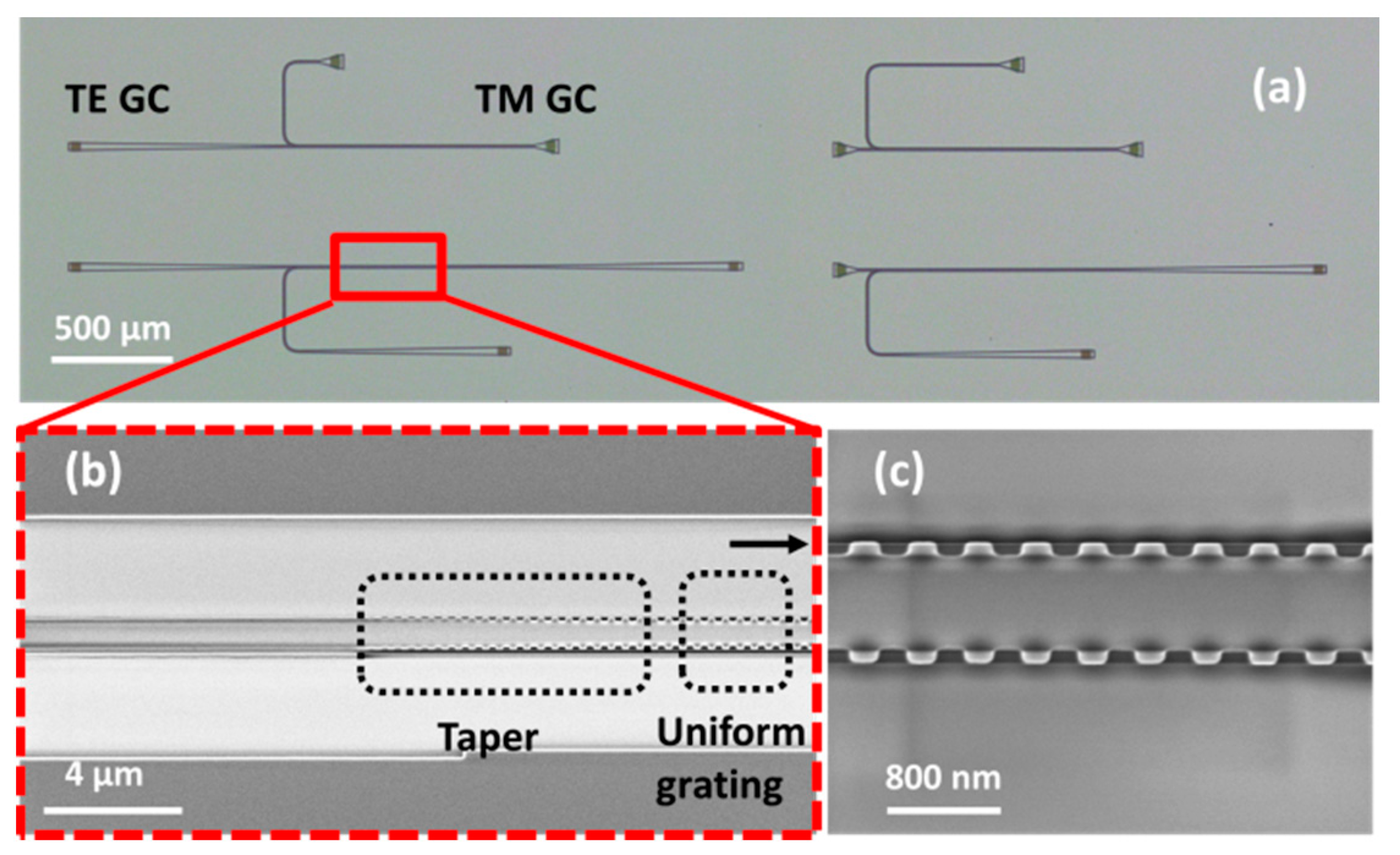
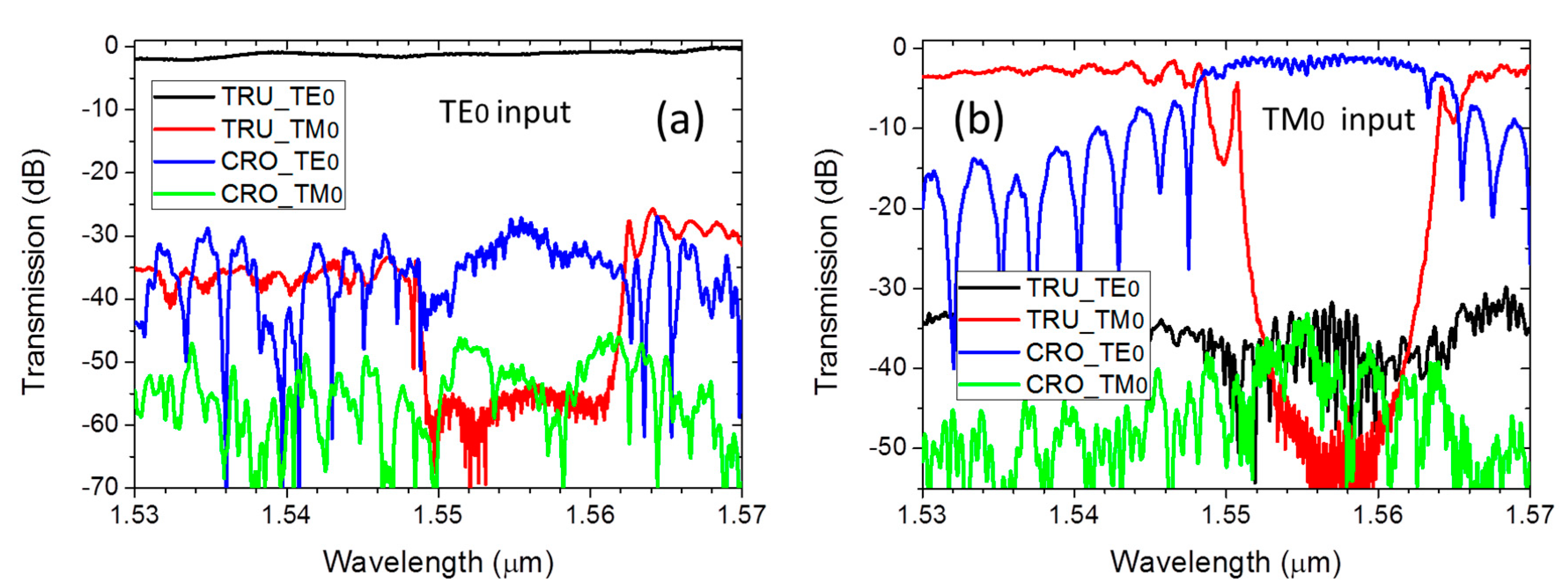
4. Fabrication and Measurement

We fabricated the proposed PSR on the SOI platform with a 220 nm thick silicon layer and a 2 μm thick oxide layer. The silicon waveguides were first patterned via electron beam lithography (EBL), then etched by the inductively coupled plasma (ICP) etching process. The focused TM grating couplers (pitch = 1.19 μm, duty cycle = 0.5) and linearly tapered TE grating couplers (pitch = 0.662 μm, duty cycle = 0.5) were adopted for fiber-chip coupling and polarization selectivity, with the same coupling angle of 20 ° . To make a full characterization for different polarization conversion scenarios, four sets of PSRs with TE/TM grating couplers at the input/output ports were fabricated, as shown in Figure 11a. It should be noted that the length of AC was chosen as 350 μm for complete mode conversion [4]. Figure 11b,c show the scanning electric microscopy (SEM) image of the taper and uniform grating section. We can see that the taper section and the designed corrugations on MWG have been accurately fabricated.
To experimentally characterize the fabricated devices, light was first generated from a C-band tunable laser, with its polarization state controlled by a polarization controller. The position and angle of the two coupling fibers were aligned utilizing two six-axis stages. The laser source and power meter were connected by a computer to implement wavelength sweeping and power data recording. Figure 12a,b show the measured transmission spectra of the fabricated PSR when TE0 mode and TM0 mode are launched, which are normalized with respect to the transmission of grating couplers on the same chip. As depicted in Figure 12a, the TE0 mode propagates to the TRU port with average IL TE of 1.2 dB. The ER TE is > 53 dB and CT TE is < −26.4 dB, around the central wavelength of 1555 nm. As shown in Figure 12b, when the TM0 mode is launched, light outputs from the CRO port; the average IL TM is 1.5 dB, ER TM of > 31 dB, and CT TM of > −30 dB can be observed ranging from 1552 nm to 1562 nm. We can also observe about 10 nm central wavelength shifting, compared with the simulation results, which comes from the fabrication errors such as the variation of waveguide width, corrugation width, or waveguide thickness.

5. Conclusions

In summary, we have presented a novel PSR based on MWG, on the SOI platform. Bloch mode hybridization in MSB is exploited to achieve a high polarization conversion efficiency. The fabricated devices exhibit a high extinction ratio of > 53 dB and > 31 dB, low crosstalk of < −26.4 dB and < −40 dB for the injected TE0 and TM0 mode around the central wavelength. We believe that the proposed PSR could be applied in integrated polarization diversity circuits, especially for applications requiring spectra manipulation such as polarization insensitive wavelength division (de)multiplexer and multichannel polarization-multiplexed differential quadrature phase-shift keying (PM-DQPSK) transceiver. Additionally, the polarization conversion approach provides opportunities to develop novel polarization management devices.

Author Contributions

Conceptualization, Y.L. (Yannong Luo) and X.C.; methodology, Y.L. (Yannong Luo), R.G. and H.L.; software, Y.L. (Yannong Luo) and R.G.; validation, Y.L. (Yannong Luo), L.Z. and M.A.; formal analysis, Y.L. (Yannong Luo), R.G. and W.L.; investigation, Y.L. (Yannong Luo) and J.Y.; resources, J.X.; data curation, Y.L. (Yannong Luo); writing—original draft preparation, Y.L. (Yannong Luo); writing—review and editing, Y.L. (Yannong Luo), M.W. and Q.L.; visualization, X.C.; supervision, Y.L. (Yongqing Li) and X.C.; project administration, Y.L. (Yannong Luo); funding acquisition, Y.L. (Yannong Luo) and X.C. All authors have read and agreed to the published version of the manuscript.

Funding

This work was supported by the National Key R&D Program of China (2019YFB1803900, 2019YFA0705000); National Natural Science Foundation of China (11690031, 11761131001, 11904061); Key R&D Program of Guangdong Province (2018B030329001); Local Innovative and Research Teams Project of Guangdong Pearl River Talents Program (2017BT01X121); Project of Key Laboratory of Radar Imaging and Microwave Photonics, Ministry of Education (RIMP2019003); Innovation Fund of WNLO (2018WNLOKF010); Guangzhou Science and Technology Program (201707010096); Guangxi youth and middle aged ability promotion project (2019KY0126); BaGui Scholar Program of Guangxi Province (02304002022C); China Postdoctoral Science Foundation (2020M673554XB); Guangdong Basic and Applied Basic Research Foundation (2020A1515010778).

Conflicts of Interest

The authors declare no conflict of interest.

References

  1. Dai, D.; Bowers, J.E. Novel concept for ultracompact polarization splitter-rotator based on silicon nanowires. Opt. Exp. 2011, 19, 10940–10949. [Google Scholar] [CrossRef] [Green Version]
  2. Dai, D.; Liu, L.; Gao, S.; Xu, D.X.; He, S. Polarization management for silicon photonic integrated circuits. Laser Photonics Rev. 2013, 7, 303–328. [Google Scholar] [CrossRef]
  3. Doerr, C.; Chen, L.; Vermeulen, D.; Nielsen, T.; Azemati, S.; Stulz, S.; McBrien, G.; Xu, X.-M.; Mikkelsen, B.; Givehchi, M. Single-chip silicon photonics 100-Gb/s coherent transceiver. In Proceedings of the Optical Fiber Communication Conference, San Francisco, CA, USA, 9–13 March 2014; p. Th5C.1. [Google Scholar]
  4. Sacher, W.D.; Barwicz, T.; Taylor, B.J.F.; Poon, J.K.S. Polarization rotator-splitters in standard active silicon photonics platforms. Opt. Exp. 2014, 22, 3777–3786. [Google Scholar] [CrossRef]
  5. Wang, Y.; Ma, M.; Yun, H.; Lu, Z.; Wang, X.; Jaeger, N.A.; Chrostowski, L. Ultra-compact sub-wavelength grating polarization splitter-rotator for silicon-on-insulator platform. IEEE Photon. J. 2016, 8, 1–9. [Google Scholar] [CrossRef]
  6. Keyvaninia, S.; Boerma, H.; Wössner, M.; Ganzer, F.; Runge, P.; Schell, M. Highly efficient passive InP polarization rotator-splitter. Opt. Exp. 2019, 27, 25872–25881. [Google Scholar] [CrossRef] [PubMed]
  7. Chung, C.-J.; Midkiff, J.; Yoo, K.M.; Rostamian, A.; Guo, J.; Chen, R.T.; Chakravarty, S. InP-based polarization rotator-splitter for mid-infrared photonic integration circuits. AIP Adv. 2019, 9, 015303. [Google Scholar] [CrossRef]
  8. Dai, X.; Lu, Q.; Guo, W. Fabrication-Tolerant Polarization Rotator-Splitter based on Silicon Nitride Platform. In Proceedings of the Optical Fiber Communication Conference, Washington, DC, USA, 6–11 June 2021; p. Th1A.31. [Google Scholar]
  9. Chen, Z.; Pan, Y.; Liu, X.; Lin, H.; Zhong, X.; Cai, X. Single-step Etching Polarization Splitter-rotator based on Lithium Niobate Ridge Waveguide. In Proceedings of the Asia Communications and Photonics Conference, Chengdu, China, 2–5 November 2019; p. M4A.285. [Google Scholar]
  10. Zhang, L.; Yang, S.; Zhang, G.; Fu, X.; Yang, L. Broadband 2 × 2 Polarization Splitter-Rotator Based on an Adiabatic Asymmetric Directional Coupler on the Lithium-Niobate-on-Insulator. In Proceedings of the Asia Communications and Photonics Conference, Beijing, China, 24–27 October 2020; p. M4A.176. [Google Scholar]
  11. Tu, X.; Li, M.; Xing, J.; Fu, H.; Geng, D. Compact PSR based on an asymmetric bi-level lateral taper in an adiabatic directional coupler. J. Light. Technol. 2016, 34, 985–991. [Google Scholar] [CrossRef]
  12. Wang, J.; Qi, M.; Xuan, Y.; Huang, H.; Li, Y.; Li, M.; Chen, X.; Jia, Q.; Sheng, Z.; Wu, A. Proposal for fabrication-tolerant SOI polarization splitter-rotator based on cascaded MMI couplers and an assisted bi-level taper. Opt. Exp. 2014, 22, 27869–27879. [Google Scholar] [CrossRef] [PubMed] [Green Version]
  13. Bai, B.; Liu, L.; Zhou, Z. Ultracompact, high extinction ratio polarization beam splitter-rotator based on hybrid plasmonic-dielectric directional coupling. Opt. Lett. 2017, 42, 4752–4755. [Google Scholar] [CrossRef] [PubMed]
  14. Chen, L.; Doerr, C.R.; Chen, Y.-K. Compact polarization rotator on silicon for polarization-diversified circuits. Opt. Lett. 2011, 36, 469–471. [Google Scholar] [CrossRef]
  15. Guan, H.; Novack, A.; Streshinsky, M.; Shi, R.; Fang, Q.; Lim, A.E.-J.; Lo, G.-Q.; Baehr-Jones, T.; Hochberg, M. CMOS-compatible highly efficient polarization splitter and rotator based on a double-etched directional coupler. Opt. Exp. 2014, 22, 2489–2496. [Google Scholar] [CrossRef] [PubMed]
  16. Dai, D.; Wu, H. Realization of a compact polarization splitter-rotator on silicon. Opt. Lett. 2016, 41, 2346–2349. [Google Scholar] [CrossRef] [PubMed]
  17. Yin, Y.; Li, Z.; Dai, D. Ultra-broadband polarization splitter-rotator based on the mode evolution in a dual-core adiabatic taper. J. Light. Technol. 2017, 35, 2227–2233. [Google Scholar] [CrossRef]
  18. Liu, L.; Ding, Y.; Yvind, K.; Hvam, J.M. Silicon-on-insulator polarization splitting and rotating device for polarization diversity circuits. Opt. Exp. 2011, 19, 12646–12651. [Google Scholar] [CrossRef] [Green Version]
  19. Ding, Y.; Liu, L.; Peucheret, C.; Ou, H. Fabrication tolerant polarization splitter and rotator based on a tapered directional coupler. Opt. Exp. 2012, 20, 20021–20027. [Google Scholar] [CrossRef] [Green Version]
  20. Tan, K.; Huang, Y.; Lo, G.-Q.; Lee, C.; Yu, C. Compact highly-efficient polarization splitter and rotator based on 90° bends. Opt. Exp. 2016, 24, 14506–14512. [Google Scholar] [CrossRef] [Green Version]
  21. Zafar, H.; Pereira, M.F.; Kennedy, K.L.; Anjum, D.H. Fabrication-tolerant and CMOS-compatible polarization splitter and rotator based on a compact bent-tapered directional coupler. AIP Adv. 2020, 10, 125214. [Google Scholar] [CrossRef]
  22. Xu, H.; Shi, Y. Ultra-broadband silicon polarization splitter-rotator based on the multi-mode waveguide. Opt. Exp. 2017, 25, 18485–18491. [Google Scholar] [CrossRef]
  23. Jeong, S.-H.; Onawa, Y.; Shimura, D.; Okayama, H.; Aoki, T.; Yaegashi, H.; Horikawa, T.; Nakamura, T. Polarization diversified 16λ demultiplexer based on silicon wire delayed interferometers and arrayed waveguide gratings. J. Light. Technol. 2020, 38, 2680–2687. [Google Scholar] [CrossRef]
  24. Onawa, Y.; Okayama, H.; Shimura, D.; Takahashi, H.; Yaegashi, H.; Sasaki, H. Polarisation insensitive wavelength de-multiplexer using arrayed waveguide grating and polarisation rotator/splitter. Electron. Lett. 2019, 55, 475–476. [Google Scholar] [CrossRef]
  25. Chen, S.; Fu, X.; Wang, J.; Shi, Y.; He, S.; Dai, D. Compact dense wavelength-division (de) multiplexer utilizing a bidirectional arrayed-waveguide grating integrated with a Mach–Zehnder interferometer. J. Light. Technol. 2015, 33, 2279–2285. [Google Scholar] [CrossRef]
  26. Olivier, S.; Rattier, M.; Benisty, H.; Weisbuch, C.; Smith, C.; De La Rue, R.; Krauss, T.; Oesterle, U.; Houdré, R. Mini-stopbands of a one-dimensional system: The channel waveguide in a two-dimensional photonic crystal. Phys. Rev. B 2001, 63, 113311. [Google Scholar] [CrossRef]
  27. Olivier, S.; Benisty, H.; Weisbuch, C.; Smith, C.J.; Krauss, T.F.; Houdré, R. Coupled-mode theory and propagation losses in photonic crystal waveguides. Opt. Exp. 2003, 11, 1490–1496. [Google Scholar] [CrossRef]
  28. Cao, T.; Cryan, M.J.; Ivanov, P.S.; Ho, D.; Ren, B.; Craddock, I.J.; Rorison, J.M.; Railton, C.J. Modeling of chirped pulse propagation through a mini-stop band in a two-dimensional photonic crystal waveguide. J. Opt. Soc. Am. B 2007, 24, 1575–1583. [Google Scholar] [CrossRef]
  29. Benisty, H.; Cambournac, C.; Van Laere, F.; Van Thourhout, D. Photonic-crystal demultiplexer with improved crosstalk by second-order cavity filtering. J. Light. Technol. 2010, 28, 1201–1208. [Google Scholar] [CrossRef]
  30. Shahid, N.; Amin, M.; Naureen, S.; Swillo, M.; Anand, S. Junction-type photonic crystal waveguides for notch-and pass-band filtering. Opt. Exp. 2011, 19, 21074–21080. [Google Scholar] [CrossRef] [PubMed]
  31. Ayre, M.; Cambournac, C.; Khayam, O.; Benisty, H.; Stomeo, T.; Krauss, T. Photonic crystal waveguides for coarse-selectivity devices. Photonics Nanostruct. 2008, 6, 19–25. [Google Scholar] [CrossRef]
  32. Moore, S.; O’Faolain, L.; White, T.; Krauss, T. Photonic crystal laser with mode selective mirrors. Opt. Exp. 2008, 16, 1365–1370. [Google Scholar] [CrossRef]
  33. Qiu, H.; Jiang, J.; Yu, P.; Yang, J.; Yu, H.; Jiang, X. Broad bandwidth and large fabrication tolerance polarization beam splitter based on multimode anti-symmetric Bragg sidewall gratings. Opt. Lett. 2017, 42, 3912–3915. [Google Scholar] [CrossRef]
  34. Huang, Q.; Jie, K.; Liu, Q.; Huang, Y.; Wang, Y.; Xia, J. Ultra-compact, broadband tunable optical bandstop filters based on a multimode one-dimensional photonic crystal waveguide. Opt. Exp. 2016, 24, 20542–20553. [Google Scholar] [CrossRef]
  35. Shi, W.; Yun, H.; Lin, C.; Greenberg, M.; Wang, X.; Wang, Y.; Fard, S.T.; Flueckiger, J.; Jaeger, N.A.; Chrostowski, L. Ultra-compact, flat-top demultiplexer using anti-reflection contra-directional couplers for CWDM networks on silicon. Opt. Exp. 2013, 21, 6733–6738. [Google Scholar] [CrossRef] [PubMed]
  36. Chen, J.; Shi, Y. Flat-Top CWDM (De) multiplexers Based on Contra-directional Couplers with Subwavelength Gratings. IEEE Photon. Technol. Lett. 2019, 31, 2003–2006. [Google Scholar] [CrossRef]
  37. Chen, L.; Doerr, C.R.; Chen, Y.-k. Polarization-diversified DWDM receiver on silicon free of polarization-dependent wavelength shift. In Proceedings of the Optical Fiber Communication Conference, Los Angeles, CA, USA, 4–8 March 2012; pp. 1–3. [Google Scholar]
  38. Corzine, S.W.; Evans, P.; Fisher, M.; Gheorma, J.; Kato, M.; Dominic, V.; Samra, P.; Nilsson, A.; Rahn, J.; Lyubomirsky, I. Large-scale InP transmitter PICs for PM-DQPSK fiber transmission systems. IEEE Photon. Technol. Lett. 2010, 22, 1015–1017. [Google Scholar] [CrossRef]
  39. Wang, X.; Wang, Y.; Flueckiger, J.; Bojko, R.; Liu, A.; Reid, A.; Pond, J.; Jaeger, N.A.; Chrostowski, L. Precise control of the coupling coefficient through destructive interference in silicon waveguide Bragg gratings. Opt. Lett. 2014, 39, 5519–5522. [Google Scholar] [CrossRef] [Green Version]
  40. Jiang, J.; Qiu, H.; Wang, G.; Li, Y.; Dai, T.; Mu, D.; Yu, H.; Yang, J.; Jiang, X. Silicon lateral-apodized add–drop filter for on-chip optical interconnection. Appl. Opt. 2017, 56, 8425–8429. [Google Scholar] [CrossRef] [PubMed]
  41. Cheng, R.; Chrostowski, L. Spectral Design of Silicon Integrated Bragg Gratings: A Tutorial. J. Light. Technol. 2020, 39, 712–729. [Google Scholar] [CrossRef]
  42. Liu, Y.; Wang, S.; Wang, Y.; Liu, W.; Xie, H.; Yao, Y.; Song, Q.; Zhang, X.; Yu, Y.; Xu, K. Subwavelength polarization splitter–rotator with ultra-compact footprint. Opt. Lett. 2019, 44, 4495–4498. [Google Scholar] [CrossRef]
Figure 1. Schematic configuration of the proposed PSR. (a) Three-dimensional structure and (b) top view of the device. (c) Architecture of polarization insensitive wavelength duplexer based on MWG-based PSRs and contra-DCs.
Crystals 11 01170 g001
Figure 2. (a) Photonic band structure of uniform MWG. (b) Local picture of MSB associated to the coupling of TM0 mode and TE1 mode. Electric field patterns associated to (c) TE1 mode (y-component, Ey) and (d) TM0 mode (z-component, Ez).
Crystals 11 01170 g002
Figure 3. (a) Transmission and reflection spectra of uniform MWG. The light propagation profiles (electric field intensity | E | ) in uniform MWG section when TE0 mode and TM0 mode are injected, at wavelengths of (b,d) 1.546 μm, (c,e) 1.509 μm, and (f) 1.496 μm.
Crystals 11 01170 g003
Figure 4. (a) The schematic of linearly tapered MWG. (b) The transmission and reflection of linearly tapered MWG as a function of min, at 1.546 μm. Calculation using the following parameters: ᴧ = 414 nm, W2 = 900 nm, δW = 100 nm, ff = 0.5, N = 10 for the uniform MWG and δwmin = 10 nm, N = 20 for the taper section.
Crystals 11 01170 g004
Figure 5. (a) The transmission and reflection spectra of linearly tapered MWG with different N. (b) TM0–TE1 conversion efficiency as a function of grating number N at 1.546 μm.
Crystals 11 01170 g005
Figure 6. (a) The reflection spectra of linearly tapered MWG with different period ᴧ. (b) The central wavelength λc and bandwidth (90% CE) as a function of grating period ᴧ at wavelength of 1.546 μm.
Crystals 11 01170 g006
Figure 7. (a) The reflection spectra of linearly tapered MWG with different corrugation width δw. (b) The central wavelength and 1 dB bandwidth as a function of δw.
Crystals 11 01170 g007
Figure 8. (a) The conversion efficiency of forward TM0 –TE1 and backward TE1–TE0, in AC section. (b) Simulated light propagation profiles (electric field intensity | E | ) in adiabatic coupler when TE1 mode propagates backward.
Crystals 11 01170 g008
Figure 9. The light propagation profiles (electric field intensity | E | ) for the PSR when (a) TE0 mode and (b) TM0 mode are launched at wavelength of 1.546 μm. The simulated transmission spectra of the proposed PSR when (c) TE0 mode and (d) TM0 mode are launched.
Crystals 11 01170 g009
Figure 10. Dependence of transmission on (a,b) width deviation ΔW2 and (c,d) corrugation width deviation Δδw for TE0 and TM0 incidence at wavelength of 1.546 μm.
Crystals 11 01170 g010
Figure 11. (a) The microscope image for the fabricated PSR. The scanning electric microscopy (SEM) image for (b) linearly taper section and (c) zoom-in of uniform grating section.
Crystals 11 01170 g011
Figure 12. (a) Measured transmission spectra of the fabricated PSRs at through port and (b) cross port when TE0 and TM0 mode are launched.
Crystals 11 01170 g012
Publisher’s Note: MDPI stays neutral with regard to jurisdictional claims in published maps and institutional affiliations.

