Article

Study on Optical and Electrical Properties of Thermally Evaporated Tin Oxide Thin Films for Perovskite Solar Cells

Department of Photonics, National Sun Yat-sen University, Kaohsiung 80424, Taiwan
*
Authors to whom correspondence should be addressed.
These authors contributed equally to this work.
Submission received: 21 October 2021 / Revised: 5 November 2021 / Accepted: 10 November 2021 / Published: 12 November 2021
(This article belongs to the Special Issue Advances of Metal Halide Perovskite Devices)

Abstract

:
Perovskite solar cells were fabricated with SnO2 thin films as a window layer and electron transport layer by thermal evaporation. Fundamental characteristics of SnO2 thin films to determine the performance of solar cells were investigated in an optical and electrical manner, varying annealing temperatures. It is found the crystallinity and the presence of localized energy states play a key factor to control the properties of SnO2. In addition, XPS was used to confirm the stoichiometry of the SnO2 thin films, indicating a better charge collection on the annealed SnO2 samples. The SnO2 thin films annealed at 300 °C exhibited desirable optical and electrical properties for the enhanced performance of solar cells. The results show that thermally evaporated SnO2 thin films can be precisely engineered and controlled for mass production and more practical industrialization of perovskite solar cells.

1. Introduction

Highly notable progress in the development of perovskite solar cells (PSCs) is not surprising news any longer. Since the pioneering work done by T. Miyasaka et al. in 2009 [1] the power conversion efficiency (PCE) of PSCs have reached over 25%, according to the chart from the National Renewable Energy Laboratory, which is comparable with that of already commercialized single crystalline silicon solar cells in the market. This successful pathway of PSCs became realized by the unique and excellent properties of perovskite such as superior absorption coefficient, the long diffusion length of the carrier, and low exciton binding energy [2,3,4,5]. A typical structure of the PSC consists of an electron transporting layer (ETL), perovskite light absorber, and hole transporting layer. The majority of excellent achievements on the performance of PCE have been achieved with modification of perovskite materials or engineering perovskite materials [6]. However, the transporting layers also take their own important role. In particular, for the so-called nip structure that is the PSC equipping with n-type semiconductor materials as window and electron transport layer, the ETL plays an essential role in the high and stable performance of the solar cells. This is because the performance of ETL is associated with light absorption of the perovskite layer and electron transport injected from perovskite. The most conventional material of the ETL is TiO2 due to its low cost and long-term stability [1,7,8]. However, its low electron mobility and high temperature process limit its application to efficient PSCs. In addition, the photocatalytic effect of TiO2 under UV light is not favorable for the stability of perovskite materials [9,10]. For these reasons, several metal oxide materials with wide bandgap have been demonstrated as alternatives, such as ZnO, SnO2, Zn2Ti3O8, BaSnO3, and α -Fe2O3 [11,12,13,14,15,16]. Among these materials, SnO2 have exhibited superiority in their properties as an efficient ETL for PSCs: 240 cm2V−1s−1 of higher electron mobility, more favorable energy band structure to perovskite, and higher transmittance with wider bandgap (3.6–4 eV) [17]. The most common way of preparing SnO2 ETL for PSCs is by solution process. The solution process innately limits surface morphology control of SnO2 compact films and the complexity of the process itself makes the fabrication of PSCs unfavorable for large scale and mass production. To solve these problems, physical vapor deposition (PVD) techniques such as sputter and evaporation would be suggested owing to its high accuracy, controllability, and easiness of operation. Yet, the study on SnO2 thin films prepared by PVD is quite insufficient and especially only a few research works have been reported on the SnO2 thin films by thermal evaporation [18,19].
In this work, we demonstrate the PSCs incorporating thermally evaporated SnO2 thin films. The material, optical and electrical properties of the SnO2 thin films are characterized, varying the annealing temperature, and studied on their relationship to the performance of the PSCs with those in a systematical manner. It is found that the crystallinity and defects influence the properties of the SnO2 films through an annealing process with various temperature and their modified properties are essential for the performance of PSCs.

2. Materials and Methods

2.1. Deposition of SnO2 Thin Films

Fluorine-doped tin oxide (FTO) glasses were sequentially cleaned with DI water, acetone, ethyl alcohol, and DI water in the ultrasonic bath for 10 min. The substrates were dried by a N2 gas gun and cleaned by UV-ozone for 30 min. SnO2 thin films were deposited on the FTO substrates with the thermal evaporator with various thicknesses. The deposition of SnO2 thin films was carried out by a thermal evaporator from SnO2 slugs (99.9% of purity) on a tungsten boat. For the deposition, the deposition rate and base pressure were 0.2 Å/s and 5 × 10⁻⁶ torr, respectively. The deposited SnO2 films were used without and with an annealing process, depending on the conditions in the ambient air for 1 h in a furnace. The prepared SnO2 thin films were subsequently treated by UV-ozone for 15 min before the deposition of perovskite on them.

2.2. Fabrication of Solar Cells with SnO2 Thin Films

For the formation of the perovskite layer, the solution was prepared with 2.3 g of PbI2, 0.8 g of Methylammonium iodide (MAI) mixed with 1.5 mL of Dimethyl sulfoxide (DMSO) and 3.5 mL of Dimethylformamide (DMF) to make the CH3NH3PbI3 solution. The perovskites were deposited on SnO2 layers via a two-step spin coating process. The perovskite films were spin-coated at 1000 rpm for 10 s and then, the final spin was at 5000 rpm for 30 s. At 5 s before the end of the final spin, 0.5 mL of Chlorobenzene (CB) was dropped on the perovskite samples. After the deposition, the samples were subject to annealing at 100 °C for 30 min and cooled down to room temperature. The hole transport layers were prepared with Poly(3-hexylthiophene-2,5-diyl) (P3HT) solution, consisted of the 20 mg of Poly(3-hexylthiophene-2,5-diyl) (P3HT) was mixed with 1 mL of CB. The P3HT films were formed by spin-coating at 2300 rpm with 30 s. Subsequently, the samples were transferred to the vacuum chamber for thermal evaporation of metal contact. The metal contacts were formed with 5 nm of MoO3 and 100 nm of Ag thin films by the thermal evaporator. The deposition rates were 0.2 Å/s and 3 Å/s for MoO3 and Ag, respectively.

2.3. Characterization

Surface morphologies of the SnO2 thin films were investigated by field emission scanning electron microscopy (FESEM, Zeiss Spura 55 from Wetzlar, Germany). X-ray diffraction (XRD, Bede D1 from Durham, UK) patterns were obtained for study on the crystal structure and crystallinity of SnO2 thin films. UV-vis spectroscopy (Shimadzu, UV-2600 I from Kyoto, Japan) was used for the optical properties of SnO2 thin film. Charge transfer characteristics were studied with photoluminescence (PL, Horiba Fluoromax) measurement. Incident photon to current measurement was carried out to evaluate the quantum efficiency of the solar cells. The performance of the solar cells was evaluated under AM 1.5 illumination (100 mW/cm2) from a solar simulator. The XPS spectra were recorded with a PHI 5000 VersaProbe system in the analytical laboratory of ULVAC-PHI, Japan. The micro-focused Al Kα X-rays (25 W, 100 μm) and the analyzer scanned an area of 400 × 400 μm2. The takeoff angle of the photoelectron was fixed at 45°. Unless otherwise stated, the XPS measurements were performed with a dual-beam charge neutralizer for charge compensation.

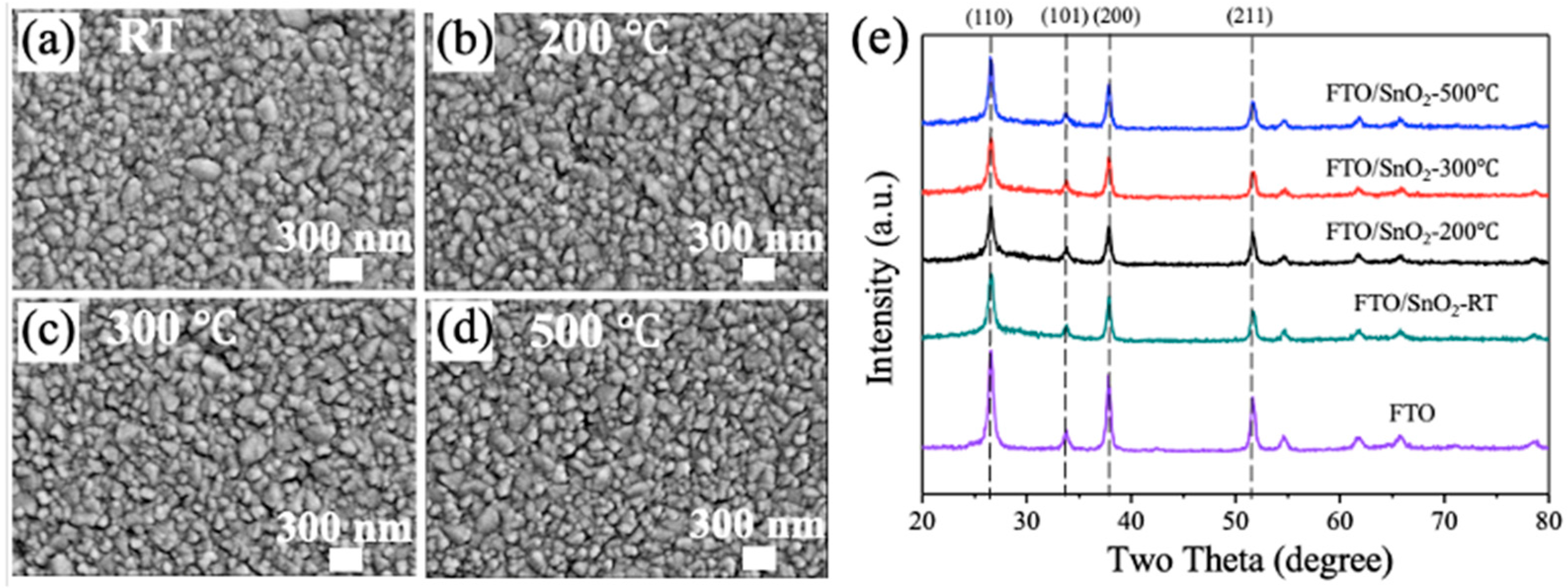
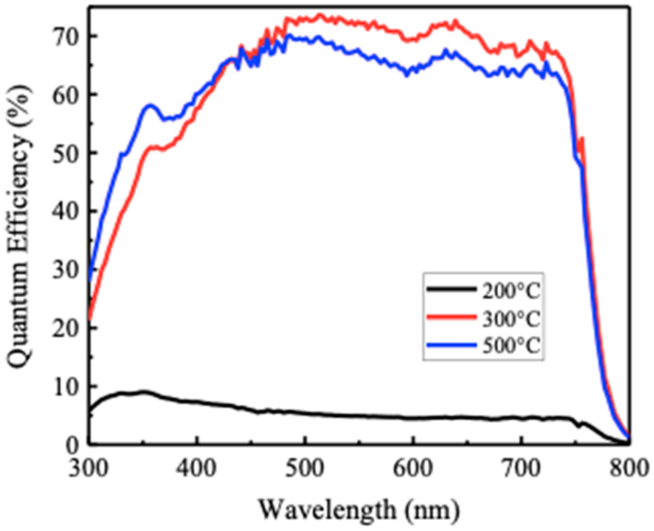
3. Results and Discussion

Figure 1a shows the surface morphologies of SnO2 thin films on FTO substrates prepared by the thermal evaporator with different annealing conditions. The SnO2 materials by thermal evaporator are uniformly deposited on FTO substrates, mimicking the surface morphologies of FTO. The remarkable difference in surface morphology is the rounded grains on the thermally evaporated SnO2 compared to the bare FTO surface (Figure S1). After the annealing process at the temperatures ranging from 200 °C to 500 °C, all the samples exhibit similar morphologies, suggesting no morphological change occurred with the annealing process. Figure 1d exhibits the XRD patterns measured from FTO and SnO2 thin films annealed at various temperatures. The deposited SnO2 films possess the same characteristic peaks to those from FTO at (110), (101), (200), and (211), as in the works done by others [20,21], showing a preferential growth orientation in (101) direction. Interestingly, all the SnO2 samples show decreased intensities in comparison with that of FTO. This suggests that the deposited SnO2 materials are less crystallized than crystallized FTO materials on the substrate. Even after the annealing process at various temperatures up to 500 °C, a high degree of crystallinity as FTO is not achievable for deposited SnO2. However, among the samples deposited with SnO2 samples, small enhancement can be observed from the intensities with the sample annealed at the higher temperature. This indicates that the annealing process still affects the crystallization of SnO2 material and, as the annealing temperature increases, it is helpful to obtain more crystallized SnO2.
The fabrication of the solar cells was implemented with these SnO2 thin films deposited through thermal evaporation. The structure of the solar cells is shown in the schematic in Figure 2a, consisting of FTO/SnO2 (160 nm)/Perovskite/P3HT/Ag. The fabricated solar cells were named as S2, S3, and S5, depending on the annealing temperatures of the SnO2 window layers. S2, S3, and S5 are the PSCs that have the SnO2 films annealed at 200 °C, 300 °C, and 500 °C, respectively, as shown in Figure 2b and Table 1. The specifications of the samples are summarized in Table 1.
The performance of the solar cells equipping three different SnO2 window layers are measured in Figure 2b both in forward and reverse scans. S3 and S5 show promising PCEs of 7.36% and 9.05%, respectively, with >20 mA/cm2 of higher Jsc while S2 exhibits almost no photovoltaic conversion performance. However, S5 exhibits more severe hysteresis characteristic in the J-V curve than that of S3, showing a similar trend to the reported work for the PSCs with solution-processed SnO2 thin films [22]. It is speculated, at the ETL/perovskite interface, interface charge accumulation can occur, and this possibly leads to electrode polarization and this polarization affects the more severe hysteric behavior of higher temperature annealed samples, namely, S5 than that of S3 [22,23]
For more understanding of the characteristics of the SnO2 films and the relationship to the performance of the solar cells, their optical properties were studied in Figure 3. All the deposited SnO2 films show higher transmittance of >80% in the visible light region but notable differences are observed from ~500 nm of wavelengths as shown in Figure 3a. The SnO2 samples annealed at higher temperatures (300 °C and 500 °C) have improved transmittance than those from the samples annealed at a lower temperature (200 °C), from ~500 nm. In addition, the SnO2 thin films exhibit more superior transmittance at <400 nm than any other samples. A similar trend is found in the Tauc plot for bandgap calculation in Figure 3b. The bandgaps of the SnO2 thin films are extracted from the equation below, [24].
α h ν = A ( h ν E g ) n
where α is the absorption coefficient, h ν is the photon energy, A is a constant, Eg is the bandgap, and n is for the modes of transitions (½ is for direct transition and 2 is for indirect transition) [24]. The calculated bandgaps of the SnO2 thin films increase as the annealing temperature increase: 2.91 eV, 3.45 eV, and 3.72 eV for 200 °C, 300 °C, and 500 °C, respectively. These results suggest that, even though there are small crystallinity variations measured in XRD in Figure 1d, the formation of band structures is affected significantly by the annealing temperature since this is probably related to localized energy states within the bandgap such as Urbach tails by crystallinity or defects due to nonstoichiometric properties of SnO2, explained in other metal oxide materials [24]. In other words, high temperature annealing help to decrease these localized energy states providing more crystallinity and more oxygen to SnO2. Considering the fact that the optical bandgap of the bulk SnO2 is around 3.6 eV, the smaller bandgap and less transmittance with lower temperature annealing are attributed to the effect from the localized energy states in the bandgaps while the larger bandgap of the sample with higher temperature is influenced by quantum confinement due to thin thickness, less presence of localized energy states, and higher crystallinity.
The existence of localized energy states and crystallinity is further proved by PL measurement in Figure 3c. The PL intensity is related to radiative recombination in the band structure of the materials from inter-band transition and the existence of localized energy states induces nonradiative recombination such as Shockley-Read-Hall recombination [25]. The SnO2 films annealed at 500 °C show higher intensity and the intensity decrease with a decrease in the annealing temperature of SnO2 thin films. This indicates that the SnO2 sample with lower temperature contains more localized energy states within their bandgaps and less crystallinity and, thereby, more non-radiative recombination is induced from PL and vice versa.
In addition, charge injection capability at the perovskite/SnO2 interface was evaluated by PL intensity measurement at ~770 nm which corresponds to the bandgap of the perovskite. Upon the excitation of perovskite materials, more quenched PL intensity is measured with the sample prepared from lower annealing temperature than that of the samples from higher annealing temperature as shown in Figure 3d. This indicates that the samples prepared at lower annealing temperatures are more favorable for efficient charge transport at SnO2/perovskite interface.
Since lower temperature annealed samples contain more localized energy states in the bandgap, this can be interpreted that the SnO2 has an Sn-rich condition, possibly due to Sn interstitial or O vacancy that is the source of the majority carrier concentration for SnO2 [20]. For further study on this, the varied concentrations of Sn elements by annealing temperatures were also measured by X-ray photoelectron spectroscopy (XPS) in Figure 4. All samples show strong peaks at ~487 eV and ~495 eV for Sn3d spectra and at ~530 eV for O1s spectra as shown in Figure 4a,b. In the Sn XPS spectra, it was found that the peak position shift from 486.2 eV to 486.9 eV, which proves the chemical state of Sn consisting of more Sn4+ state. A decrease in Sn ratio in composition was observed with increasing annealing temperature and the sample annealed at 500 °C was measured with the minimum value, suggesting the carrier concentration decreases with increasing annealing temperature (Figure 4c). In another view, the Fermi level becomes closer with decreasing temperature because the carrier concentration increase, suggesting the formation of a lower work function of SnO2. Moreover, according to previous works, the conduction band edge can be shifted downward with a higher temperature annealing process [26,27]. Considering these two findings, the samples prepared at lower annealing temperature are more favorable obtaining more driving forces by the larger difference of Fermi levels between SnO2 and perovskite for electron transfer from perovskite to SnO2. This trend is well matched to the results of PL in Figure 3d, and it proves that the samples prepared with lower annealing temperature are more favorable efficient charge injection from perovskite to SnO2 for the improved performance of solar cells.
Another interesting finding was measured from incident photon to current (IPCE) measurement as plotted in Figure 5. No promising performance is measured with S2, reflecting Jsc in Table 1, but S3 and S5 represent enhanced IPCE in entire absorption wavelengths. In particular, S3 shows more enhanced IPCE in longer wavelengths of >450 nm while S5 produces more IPCE in shorter wavelengths of <450 nm. In general, IPCE in longer wavelengths is related to the carrier diffusion while IPCE in shorter wavelengths is related to surface recombination. In other words, S5 exhibits less surface recombination while S3 shows better carrier transport properties. Moreover, no further performance improvement for S5 was measured even with the optimization process based on the thickness (Figure S2 and Table S1). Again, these are possibly resulted from that the innate feature of SnO2 materials and localized energy states mentioned above. SnO2 is commonly accepted as n-type material because SnO2 easily shows nonstoichiometric characteristics between Sn and S elements. These nonstoichiometric characteristics are related to the presence of defects either owing to tin interstitials or oxygen vacancies and those act as sources of the majority carrier, electron [20,28]. These results are well corresponded to previous results from XRD, UV-vis spectroscopy, and PL in Figure 2 and Figure 4. Therefore, it is possible that, depending on the control of defect concentration, the charge transport can be accelerated or be disturbed, accelerating, or suppressing the nonradiative recombination within the materials and controlling bandgap with the distribution of Urbach tails [24]. That is, SnO2 thin films with lower temperature annealing can be more conductive than those with higher temperature but those would have a higher density of defects at the same time.
In these contexts, S3 solar cells were considered a more desirable candidate for further study due to its excellent charge injection, transport, and transparency. Therefore, subsequent optimization was focused on S3 samples, varying the thicknesses of SnO2.
Figure 6a and Table 2 show the performance measured from the solar cells adopting three different thicknesses of the SnO2 thin films annealed at 300 °C: 70 nm (S3–70), 100 nm (S3–100), and 160 nm (S3). The protruding findings from the results were obtained from S3–100, together with nearly completed perovskite conversion in its crystal structure in Figure S2, recording the enhancement in all the photovoltaic parameters: namely, Jsc, Voc, FF, and PCE. In particular, the performance itself is higher than the optimized S5 samples in terms of the thickness of SnO2. as shown in Figure S3 and Table S1 in the Supporting Information. This probably results from several benefits from the reduced thickness of the window layer and features of SnO2 annealed at 300 °C. However, further decrease in the thickness has no contribution to the performance enhancement possibly due to the existence of a pinhole that can make a short circuit between FTO substrate and perovskite light absorber [24]. To find out the features from the reduced thickness of the window layer and the effect of annealing at 300 °C for notable performance enhancement of S3–100 by thickness and annealing at 300 °C, optical properties were firstly examined by UV-vis spectroscopy from deposited SnO2 films in Figure 6b. The SnO2 thin films with thickness variations show improved transmittance in the whole spectrum and the shift in transmission spectrum to longer wavelengths with thicker films, indicating optical bandgap shift. This improved transmittance can allow more efficient light penetration to the perovskite light absorber, which is advantageous in obtaining higher Jsc in Figure 6 and Table 2. In addition, more crystallized SnO2 materials, being evidenced by the shift in their optical bandgaps in Figure 6b, facilitate the charge transport through SnO2. Except for the large resistances probably due to unwanted flow of charge by structurally defective SnO2 thin films of S3–70, S3–100 is measured with reduced series resistance (Rs) of 161 Ω and increased shunt resistance (Rsh) of 3602 Ω in Table 2. The improved Rs can facilitate the efficient charge transport through SnO2 bulk materials and enhanced Rsh prevents severe leakage of current. FF can be improved due to improved series resistance through SnO2 film. All these advantages led S3–100 to higher performance of solar cells.

4. Conclusions

In conclusion, thermally evaporated SnO2 thin films were employed for efficient window and charge transport layer for PSCs. The PSCs incorporating the SnO2 thin films prepared at different annealing temperatures exhibited variation in their performance. It is found that varying annealing temperatures are effective in the control of optical and electrical properties, influencing its crystallinity, chemical state, and the distribution of localized energy state. Among the samples, the PSCs equipping the SnO2 thin films annealed at 300 °C showed more desirable performance owing to simultaneously improved optical and electrical properties. With further optimization in the thickness, the PSC equipping with the thermally evaporated SnO2 films represent a promising performance of >10% PCE with further increased transmittance and improved electrical properties. This work would provide the background knowledge for the optimization of the performance for more efficient mass production, and this would pave the way to make more practical commercialization of PSC in near future.

Supplementary Materials

The following are available online at https://0-www-mdpi-com.brum.beds.ac.uk/article/10.3390/cryst11111380/s1, Figure S1: Surface morphology of FTO substrate by SEM, Figure S2: X-ray diffraction pattern for the perovskite films on the 100nm-thick SnO2 films annealed at 300°C, Figure S3: The J-V curve of PSCs with 500 °C annealed SnO2 with varied thickness, Table S1: The performance of PSCs with 500 °C annealed SnO2 with varied thickness.

Author Contributions

H.L. and W.-C.L. conceived idea and designed the experiments. W.-M.B. and W.-H.H. prepared the materials and performed the experiments. All authors analyzed data and participated in manuscript writing and revision. All authors have read and agreed to the published version of the manuscript.

Funding

This work is supported by the Ministry of Science and Technology of Taiwan under projects no. MOST 109-2218-E-110-005-MY2, MOST 110-2221-E-110-042, MOST 108-2113-M-035-002-MY2, and MOST 110-2113-M-110-024.

Data Availability Statement

Not applicable.

Acknowledgments

The authors acknowledge instrument support from Analytical Lab, ULVAC-PHI and the XPS measurement done by Hsun-Yun Chang.

Conflicts of Interest

The authors declare that they have no conflict of interest.

References

  1. Kojima, A.; Teshima, K.; Shirai, Y.; Miyasaka, T. Organometal Halide Perovskites as Visible-Light Sensitizers for Photovoltaic Cells. J. Am. Chem. Soc. 2009, 131, 6050–6051. [Google Scholar] [CrossRef]
  2. Green, M.A.; Ho-Baillie, A.; Snaith, H. The emergence of perovskite solar cells. Nat. Photonics 2014, 8, 506–514. [Google Scholar] [CrossRef]
  3. Miyata, A.; Mitioglu, A.; Plochocka, P.; Portugall, O.; Wang, J.T.-W.; Stranks, S.D.; Snaith, H.; Nicholas, R. Direct measurement of the exciton binding energy and effective masses for charge carriers in organic-inorganic tri-halide perovskites. Nat. Phys. 2015, 11, 582–587. [Google Scholar] [CrossRef] [Green Version]
  4. Dong, Q.; Fang, Y.; Shao, Y.; Mulligan, P.; Qiu, J.; Cao, L.; Huang, J. Electron-hole diffusion lengths >175 μm in solution-grown CH3NH3PbI3single crystals. Science 2015, 347, 967–970. [Google Scholar] [CrossRef] [Green Version]
  5. Nie, W.; Tsai, H.; Asadpour, R.; Blancon, J.-C.; Neukirch, A.J.; Gupta, G.; Crochet, J.J.; Chhowalla, M.; Tretiak, S.; Alam, M.A.; et al. High-efficiency solution-processed perovskite solar cells with millimeter-scale grains. Science 2015, 347, 522–525. [Google Scholar] [CrossRef] [PubMed] [Green Version]
  6. Kim, J.Y.; Lee, J.-W.; Jung, H.S.; Shin, H.; Park, N.-G. High-Efficiency Perovskite Solar Cells. Chem. Rev. 2020, 120, 7867–7918. [Google Scholar] [CrossRef]
  7. Kim, H.-S.; Lee, C.-R.; Im, J.-H.; Lee, K.-B.; Moehl, T.; Marchioro, A.; Moon, S.-J.; Humphry-Baker, R.; Yum, J.-H.; Moser, J.E.; et al. Lead Iodide Perovskite Sensitized All-Solid-State Submicron Thin Film Mesoscopic Solar Cell with Efficiency Exceeding 9%. Sci. Rep. 2012, 2, 591. [Google Scholar] [CrossRef] [Green Version]
  8. Lee, M.M.; Teuscher, J.; Miyasaka, T.; Murakami, T.N.; Snaith, H.J. Efficient Hybrid Solar Cells Based on Meso-Superstructured Organometal Halide Perovskites. Science 2012, 338, 643–647. [Google Scholar] [CrossRef] [PubMed] [Green Version]
  9. Leijtens, T.; Eperon, G.; Pathak, S.; Abate, A.; Lee, M.M.; Snaith, H. Overcoming ultraviolet light instability of sensitized TiO2 with meso-superstructured organometal tri-halide perovskite solar cells. Nat. Commun. 2013, 4, 2885. [Google Scholar] [CrossRef] [PubMed]
  10. Omr, H.A.; Horn, M.W.; Lee, H. Low-Dimensional Nanostructured Photocatalysts for Efficient CO2 Conversion into Solar Fuels. Catalysts 2021, 11, 418. [Google Scholar] [CrossRef]
  11. An, Q.; Fassl, P.; Hofstetter, Y.J.; Becker-Koch, D.; Bausch, A.; Hopkinson, P.E.; Vaynzof, Y. High performance planar perovskite solar cells by ZnO electron transport layer engineering. Nano Energy 2017, 39, 400–408. [Google Scholar] [CrossRef]
  12. Zhang, P.; Wu, J.; Zhang, T.; Wang, Y.; Liu, D.; Chen, H.; Jiang, W.; Liu, C.; Ahmad, W.; Chen, Z.D.; et al. Perovskite Solar Cells with ZnO Electron-Transporting Materials. Adv. Mater. 2018, 30, 1703737. [Google Scholar] [CrossRef]
  13. Wu, P.; Wang, S.; Li, X.; Zhang, F. Advances in SnO2-based perovskite solar cells: From preparation to photovoltaic applications. J. Mater. Chem. A 2021, 9, 19554–19588. [Google Scholar] [CrossRef]
  14. Pang, A.; Shen, D.; Wei, M.; Chen, Z.-N. Highly Efficient Perovskite Solar Cells Based on Zn2 Ti3 O8 Nanoparticles as Electron Transport Material. ChemSusChem 2018, 11, 424–431. [Google Scholar] [CrossRef]
  15. Sun, C.; Guan, L.; Guo, Y.; Fang, B.; Yang, J.; Duan, H.; Chen, Y.; Li, H.; Liu, H. Ternary oxide BaSnO3 nanoparticles as an efficient electron-transporting layer for planar perovskite solar cells. J. Alloys Compd. 2017, 722, 196–206. [Google Scholar] [CrossRef]
  16. Hou, Q.; Ren, J.; Chen, H.; Yang, P.; Shao, Q.; Zhao, M.; Zhao, X.; He, H.; Wang, N.; Luo, Q.; et al. Synergistic Hematite-Fullerene Electron-Extracting Layers for Improved Efficiency and Stability in Perovskite Solar Cells. ChemElectroChem 2018, 5, 726–731. [Google Scholar] [CrossRef]
  17. Jiang, Q.; Zhao, Y.; Zhang, X.; Yang, X.; Chen, Y.; Chu, Z.; Ye, Q.; Li, X.; Yin, Z.; You, J. Surface passivation of perovskite film for efficient solar cells. Nat. Photonics 2019, 13, 460–466. [Google Scholar] [CrossRef]
  18. Guo, Y.; Yin, X.; Liu, J.; Chen, W.; Wen, S.; Que, M.; Xie, H.; Yang, Y.; Que, W.; Gao, B. Vacuum thermal-evaporated SnO2 as uniform electron transport layer and novel management of perovskite intermediates for efficient and stable planar perovskite solar cells. Org. Electron. 2019, 65, 207–214. [Google Scholar] [CrossRef]
  19. Kam, M.; Zhang, Q.; Zhang, D.; Fan, Z. Room-Temperature Sputtered SnO2 as Robust Electron Transport Layer for Air-Stable and Efficient Perovskite Solar Cells on Rigid and Flexible Substrates. Sci. Rep. 2019, 9, 6963. [Google Scholar] [CrossRef] [PubMed]
  20. Porte, Y.; Maller, R.; Faber, H.; AlShareef, H.N.; Anthopoulos, T.D.; McLachlan, M.A. Exploring and controlling intrinsic defect formation in SnO2 thin films. J. Mater. Chem. C 2016, 4, 758–765. [Google Scholar] [CrossRef] [Green Version]
  21. Jeong, S.; Seo, S.; Park, H.; Shin, H. Atomic layer deposition of a SnO2 electron-transporting layer for planar perovskite solar cells with a power conversion efficiency of 18.3%. Chem. Commun. 2019, 55, 2433–2436. [Google Scholar] [CrossRef] [PubMed]
  22. Jung, K.-H.; Seo, J.-Y.; Lee, S.; Shin, H.; Park, N.-G. Solution-processed SnO2 thin film for a hysteresis-free planar perovskite solar cell with a power conversion efficiency of 19.2%. J. Mater. Chem. A 2017, 5, 24790–24803. [Google Scholar] [CrossRef]
  23. Chen, B.; Yang, M.; Priya, S.; Zhu, K. Origin of J-V Hysteresis in Perovskite Solar Cells. J. Phys. Chem. Lett. 2016, 7, 905–917. [Google Scholar] [CrossRef]
  24. Lee, H.; Huang, Y.-T.; Horn, M.W.; Feng, S.-P. Engineered optical and electrical performance of rf-sputtered undoped nickel oxide thin films for inverted perovskite solar cells. Sci. Rep. 2018, 8, 5590. [Google Scholar] [CrossRef] [PubMed]
  25. Neamen, D.A. Semiconductor Physics and Devices; McGraw Hill: New York, NY, USA; Springer: Berlin/Heidelberg, Germany, 1992. [Google Scholar]
  26. Kavan, L.; Steier, L.; Grätzel, M. Ultrathin Buffer Layers of SnO2 by Atomic Layer Deposition: Perfect Blocking Function and Thermal Stability. J. Phys. Chem. C 2017, 121, 342–350. [Google Scholar] [CrossRef]
  27. Lee, Y.; Lee, S.; Seo, G.; Paek, S.; Cho, K.T.; Huckaba, A.; Calizzi, M.; Choi, D.-W.; Park, J.-S.; Lee, D.; et al. Efficient Planar Perovskite Solar Cells Using Passivated Tin Oxide as an Electron Transport Layer. Adv. Sci. 2018, 5, 1800130. [Google Scholar] [CrossRef]
  28. Kılıç, Ç.; Zunger, A. Origins of coexistence of conductivity and transparency in SnO2. Phys. Rev. Lett. 2002, 88, 095501. [Google Scholar] [CrossRef] [Green Version]
Figure 1. Surface morphologies of FTO/SnO2 thin films (a) at RT and annealed at (b) 200 °C (c) 300 °C (d) 500 °C by field emission scanning electron microscope. (e) X-ray diffraction patterns of FTO and FTO/SnO2 thin films annealed at various temperatures. RT stands for room temperature. RT stands for room temperature.
Crystals 11 01380 g001
Figure 2. (a) The structure of the PSC fabricated here (b) the J-V curve of the PSCs with 160 nm-thick SnO2 thin films, depending on annealing temperature variation.
Crystals 11 01380 g002
Figure 3. Characteristics of the SnO2 thin films annealed at various temperatures: (a) normalized transmittance spectra (b) Tauc plots, and (c) PL spectra without and (d) with a perovskite layer.
Crystals 11 01380 g003
Figure 4. X-ray photoelectron spectroscopy spectra of FTO/SnO2 samples annealed at various temperatures for (a) Sn, (b) O, and (c) extracted atomic ratio of Sn.
Crystals 11 01380 g004
Figure 5. IPCE measurement of the perovskite solar cells equipped with the SnO2 thin films prepared at various annealing temperature.
Crystals 11 01380 g005
Figure 6. (a) J-V characteristics of PSC incorporating SnO2 thin films with different thicknesses (b) the transmittance spectra of the SnO2 thin films with varied thicknesses. The SnO2 was annealed at 300 °C and, for the transmittance measurement, SnO2/FTO samples were used.
Crystals 11 01380 g006
Table 1. The performance of PSCs with 160 nm-thick SnO2 thin films, depending on annealing temperature variation.
Sample NamesAnnealing Temperature (°C)Scan DirectionJsc (mA/cm2)Voc (mV)Fill FactorPCE (%)
S2200F3.525300.100.18
R3.386580.160.35
S3300F21.668610.285.21
R20.819100.397.36
S5500F16.587740.405.17
R21.718160.519.05
Table 2. The performance of PSCs with 300 °C annealed SnO2 with varied thickness.
Sample NamesThickness of SnO2 (nm)Jsc (mA/cm2)Voc (mV)Fill FactorPCE (%)Rs (Ω)Rsh (Ω)
S3–70700.246720.550.09697086,155
S3–10010022.409310.5110.651613602
S316020.819100.397.362572542
Publisher’s Note: MDPI stays neutral with regard to jurisdictional claims in published maps and institutional affiliations.

