
The Effect of Annealing on the Optoelectronic Properties and Energy State of Amorphous Pyrochlore Y2Ti2O7 Thin Layers by Sol–Gel Synthesis

 , , and
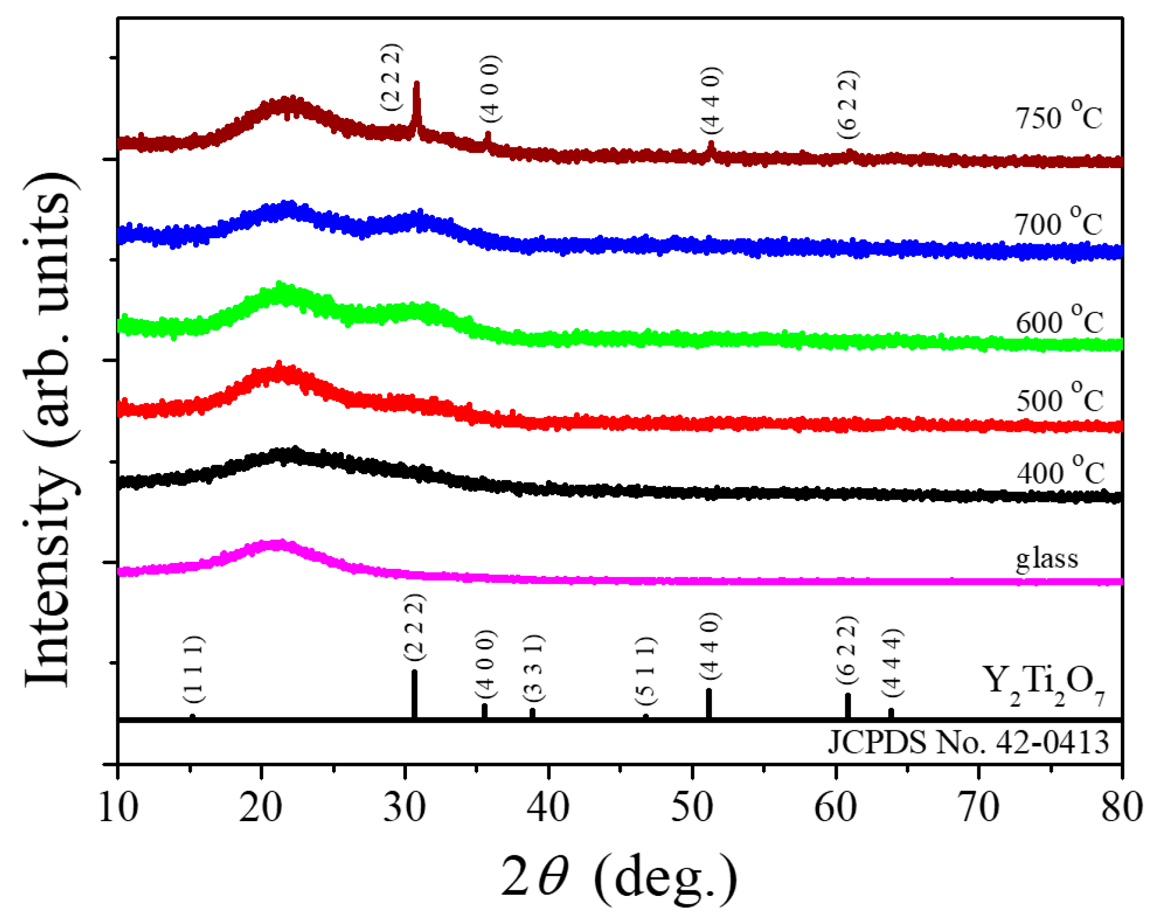
Abstract
:1. Introduction
2. Experimental Procedures
2.1. Fabrication of Sol–Gel Solution and Thin Layers
2.2. Characterization of Thin Layers
3. Results and Discussion
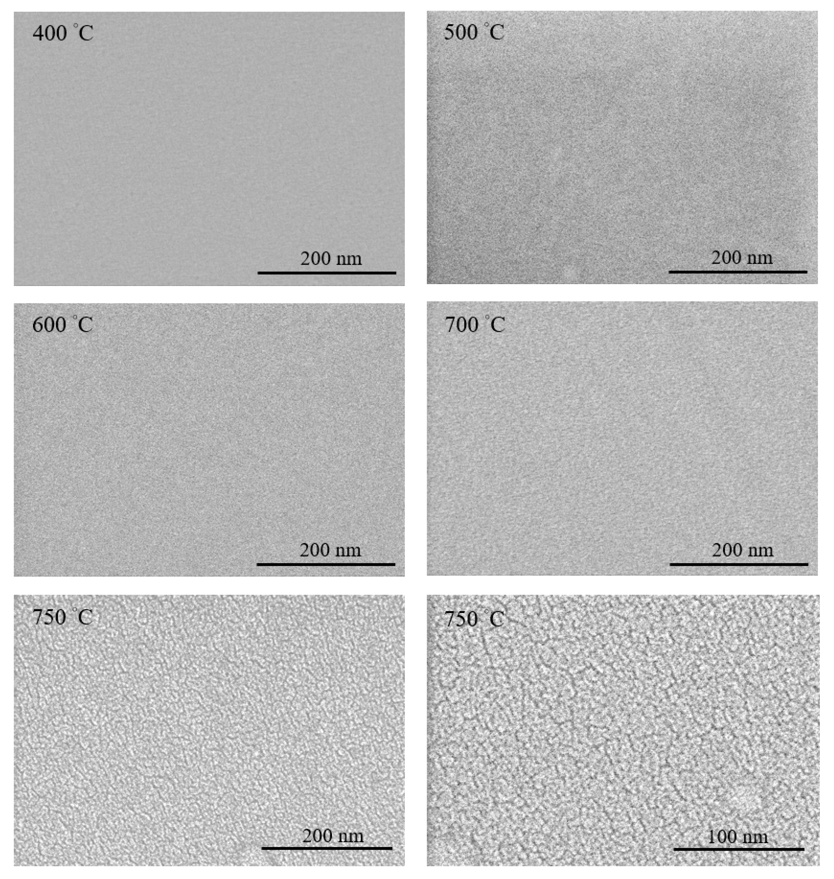
3.1. Crystal Structure and Layer Morphology
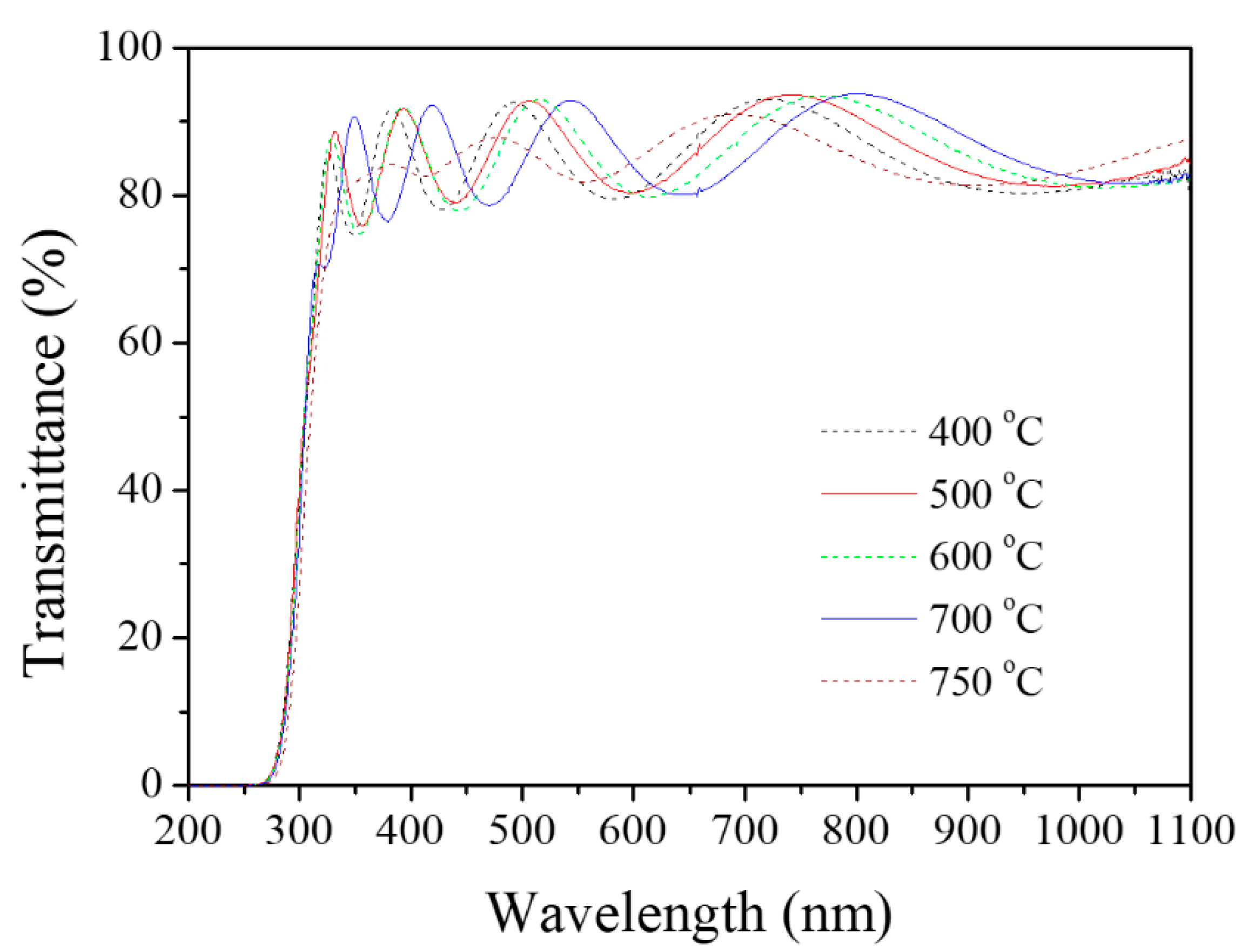
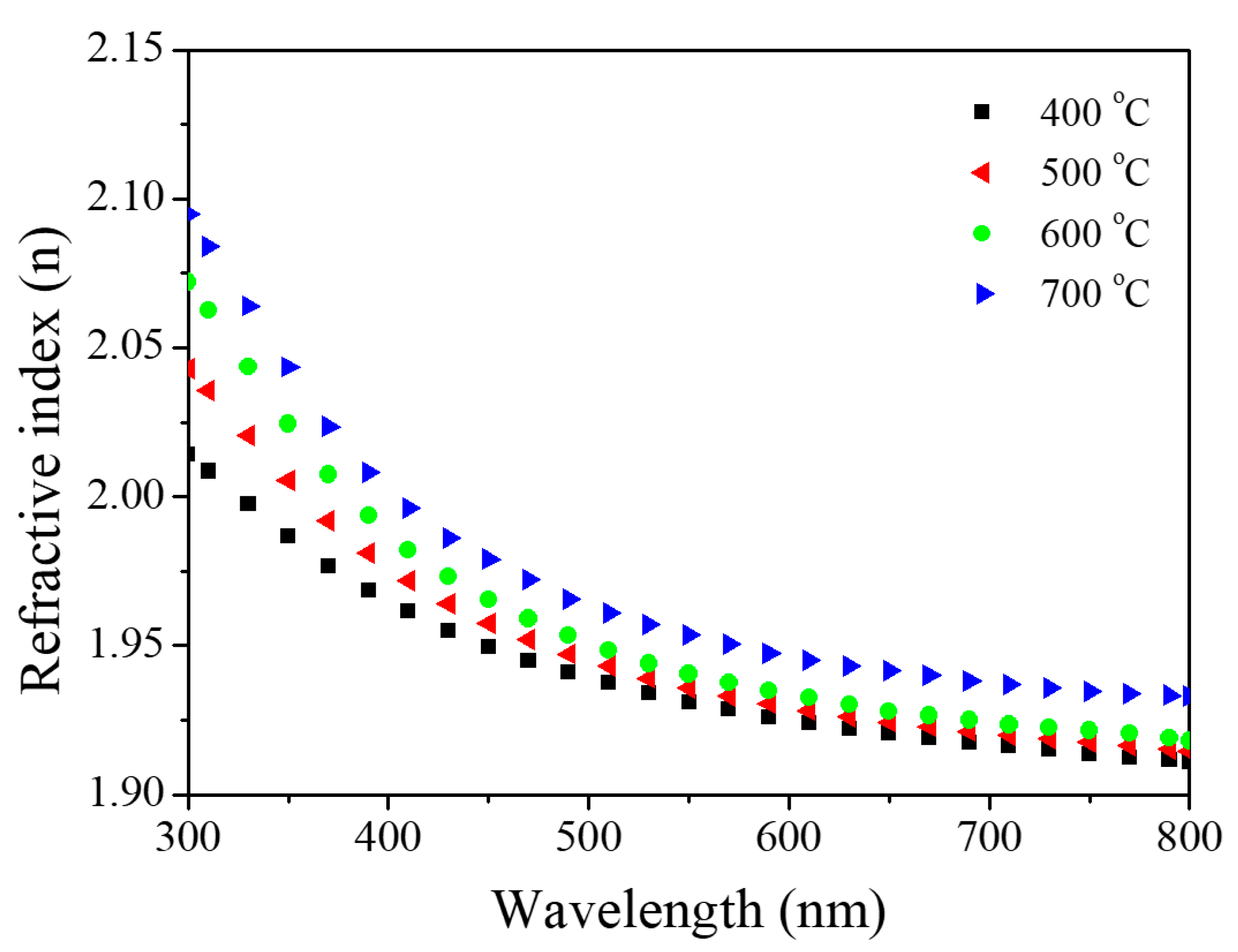
3.2. Optoelectronic Properties
4. Conclusions
Author Contributions
Funding
Institutional Review Board Statement
Informed Consent Statement
Data Availability Statement
Conflicts of Interest
References
- Suganya, M.; Ganesan, K.; Vijayakumar, P.; Gill, A.S.; Ramaseshan, R.; Ganesamoorthy, S. Structural, optical and mechanical properties of Y2Ti2O7 single crystal. Scr. Mater. 2020, 187, 227–231. [Google Scholar] [CrossRef]
- Zhao, H.; Liu, T.; Bai, Z.; Wang, L.; Gao, W.; Zhang, L. Corrosion behavior of 14Cr ODS steel in supercritical water: The influence of substituting Y2O3 with Y2Ti2O7 nanoparticles. Corros. Sci. 2020, 163, 108272. [Google Scholar] [CrossRef]
- Badjeck, V.; Walls, M.; Chaffron, L.; Malaplate, J.; March, K. New insights into the chemical structure of Y2Ti2O7− δ nanoparticles in oxide dispersion-strengthened steels designed for sodium fast reactors by electron energy-loss spectroscopy. J. Nucl. Mater. 2015, 456, 292–301. [Google Scholar] [CrossRef]
- Lai, F.; Cheng, H.; Jiang, Z.; Liu, C.; Liang, T.; You, W. Manipulation of upconversion property and enhancement of sensitivity by tailoring the local structure. J. Am. Ceram. Soc. 2021, 104, 369–382. [Google Scholar] [CrossRef]
- Dai, P.; Zhang, X.; Zhou, M.; Li, X.; Yang, J.; Sun, P.; Xu, C.; Liu, Y. Thermally stable pyrochlore Y2Ti2O7: Eu3+ orange–red emitting phosphors. J. Am. Ceram. Soc. 2012, 95, 658–662. [Google Scholar] [CrossRef]
- Yu, X.; Zhao, T.; Wang, T.; Bao, W.; Zhang, H.; Su, C. Up-conversion luminescence properties of Ho3+-Yb3+ Co-doped transparent glass ceramics containing Y2Ti2O7. J. Non-Cryst. Solids 2021, 574, 121163. [Google Scholar] [CrossRef]
- Merka, O.; Bahnemann, D.W.; Wark, M. Improved photocatalytic hydrogen production by structure optimized nonstoichiometric Y2Ti2O7. ChemCatChem 2012, 4, 1819–1827. [Google Scholar] [CrossRef]
- Wang, Z.; Wang, X.; Zhou, G.; Xie, J.; Wang, S. Highly transparent yttrium titanate (Y2Ti2O7) ceramics from co-precipitated powders. J. Eur. Ceram. Soc. 2019, 39, 3229–3234. [Google Scholar] [CrossRef]
- Yamaguchi, S.; Kobayashi, K.; Abe, K.; Yamazaki, S.; Iguchi, Y. Electrical conductivity and thermoelectric power measurements of Y2Ti2O7. Solid State Ion. 1998, 113, 393–402. [Google Scholar] [CrossRef]
- Gill, J.K.; Pandey, O.; Singh, K. Ionic conductivity, structural and thermal properties of pure and Sr2+ doped Y2Ti2O7 pyrochlores for SOFC. Solid State Sci. 2011, 13, 1960–1966. [Google Scholar] [CrossRef]
- Abe, R.; Higashi, M.; Zou, Z.; Sayama, K.; Abe, Y. Photocatalytic water splitting into H2 and O2 over R2Ti2O7 (R = Y, rare earth) with pyrochlore structure. Chem. Lett. 2004, 33, 954–955. [Google Scholar] [CrossRef]
- Gill, J.K.; Pandey, O.; Singh, K. Ionic conductivity, structural and thermal properties of Ca2+ doped Y2Ti2O7 pyrochlores for SOFC. Int. J. Hydrogen Energy 2012, 37, 3857–3864. [Google Scholar] [CrossRef]
- Higashi, M.; Abe, R.; Sayama, K.; Sugihara, H.; Abe, Y. Improvement of photocatalytic activity of titanate pyrochlore Y2Ti2O7 by addition of excess Y. Chem. Lett. 2005, 34, 1122–1123. [Google Scholar] [CrossRef]
- Mahapatra, A.; Subudhi, S.; Swain, S.; Sahu, R.; Negi, R.; Samanta, B.; Kumar, P. Electrical and optical properties of yttrium titanate thin films synthesized by Sol-Gel technique. Integr. Ferroelectr. 2019, 203, 43–51. [Google Scholar] [CrossRef]
- Wen, Q.; Zhou, W.; Gao, H.; Zhou, Y.; Luo, F.; Zhu, D.; Huang, Z.; Qing, Y. Enhanced dielectric and microwave absorption properties of Y2Ti2O7 ceramics by Sr doping. Appl. Phys. A 2019, 125, 413. [Google Scholar] [CrossRef]
- Öztürk, E.; Sarılmaz, E. The investigation of the photoluminescent and piezoelectric effect of Eu3+ doped Y2Ti2O7 and Sm2Ti2O7 host crystals. Mater. Chem. Phys. 2020, 239, 122085. [Google Scholar] [CrossRef]
- Li, W.; Chuah, C.Y.; Yang, Y.; Bae, T.-H. Nanocomposites formed by in situ growth of NiDOBDC nanoparticles on graphene oxide sheets for enhanced CO2 and H2 storage. Microporous Mesoporous Mater. 2018, 265, 35–42. [Google Scholar] [CrossRef]
- Pace, S.; Cannillo, V.; Wu, J.; Boccaccini, D.; Seglem, S.; Boccaccini, A. Processing glass–pyrochlore composites for nuclear waste encapsulation. J. Nucl. Mater. 2005, 341, 12–18. [Google Scholar] [CrossRef]
- Goodenough, J.; Castellano, R. Defect pyrochlores as catalyst supports. J. Solid State Chem. 1982, 44, 108–112. [Google Scholar] [CrossRef]
- Munawar, K.; Mansoor, M.A.; Olmstead, M.M.; Yusof, F.B.; Misran, M.B.; Basirun, W.J.; Mazhar, M. Pyrochlore-structured Y2Ti2O7–2TiO2 composite thin films for photovoltaic applications. J. Aust. Ceram. Soc. 2019, 55, 921–932. [Google Scholar] [CrossRef]
- Mondal, K.; Hartman, K.; Dasgupta, D.; Trifon, G.; Dasari, M. Synthesis and characterization of Y2Ti2O7 and ErxY2−xTi2O7 nanofibers. J. Sol-Gel Sci. Technol. 2015, 73, 265–269. [Google Scholar] [CrossRef]
- Jenouvrier, P.; Boccardi, G.; Fick, J.; Jurdyc, A.-M.; Langlet, M. Up-conversion emission in rare earth-doped Y2Ti2O7 sol–gel thin films. J. Lumin. 2005, 113, 291–300. [Google Scholar] [CrossRef]
- Jenouvrier, P.R.; Langlet, M.; Fick, J. High photoluminescence in a new nanocrystalline active phase: YETO. In Proceedings of the Sol-Gel Optics VI. International Symposium on Optical Science and Technology, Seattle, WA, USA, 23 October 2002; pp. 52–59. [Google Scholar]
- Tu, X.; Xu, J.; Li, M.; Xie, T.; Lei, R.; Wang, H.; Xu, S. Color-tunable upconversion luminescence and temperature sensing behavior of Tm3+/Yb3+ codoped Y2Ti2O7 phosphors. Mater. Res. Bull. 2019, 112, 77–83. [Google Scholar] [CrossRef]
- Huang, X.; Huang, K.; Chen, L.; Chen, N.; Lei, R.; Zhao, S.; Xu, S. Effect of Li+/Mg2+ co-doping and optical temperature sensing behavior in Y2Ti2O7: Er3+/Yb3+ upconverting phosphors. Opt. Mater. 2020, 107, 110114. [Google Scholar] [CrossRef]
- Reisfeld, R.; Saraidarov, T.; Panzer, G.; Levchenko, V.; Gaft, M. New optical material europium EDTA complex in polyvinyl pyrrolidone films with fluorescence enhanced by silver plasmons. Opt. Mater. 2011, 34, 351–354. [Google Scholar] [CrossRef]
- Henkes, A.E.; Bauer, J.C.; Sra, A.K.; Johnson, R.D.; Cable, R.E.; Schaak, R.E. Low-temperature nanoparticle-directed solid-state synthesis of ternary and quaternary transition metal oxides. Chem. Mater. 2006, 18, 567–571. [Google Scholar] [CrossRef]
- Lee, W.J.; Bae, D.S. Synthesis and Characterization of Y2Ti2O7 Photocatalytic Powders by Thermal Assist Process. Defect Diffus. Forum 2017, 380, 86–91. [Google Scholar] [CrossRef]
- Gadipelly, T.; Dasgupta, A.; Ghosh, C.; Krupa, V.; Sornadurai, D.; Sahu, B.K.; Dhara, S. Synthesis and structural characterisation of Y2Ti2O7 using microwave hydrothermal route. J. Alloys Compd. 2020, 814, 152273. [Google Scholar] [CrossRef]
- Fuentes, A.F.; Boulahya, K.; Maczka, M.; Hanuza, J.; Amador, U. Synthesis of disordered pyrochlores, A2Ti2O7 (A = Y, Gd and Dy), by mechanical milling of constituent oxides. Solid State Sci. 2005, 7, 343–353. [Google Scholar] [CrossRef]
- Simondon, E.; Giroux, P.-F.; Chaffron, L.; Fitch, A.; Castany, P.; Gloriant, T. Mechanical synthesis of nanostructured Y2Ti2O7 pyrochlore oxides. Solid State Sci. 2018, 85, 54–59. [Google Scholar] [CrossRef]
- Dimesso, L. Pechini processes: An alternate approach of the sol–gel method, preparation, properties, and applications. Handb. Sol-Gel Sci. Technol. 2016, 2, 1–22. [Google Scholar]
- Wang, S.; Wang, L.; Ewing, R.; Kutty, K.G. Ion irradiation of rare-earth-and yttrium-titanate-pyrochlores. Nucl. Instrum. Methods Phys. Res. Sect. B Beam Interact. Mater. At. 2000, 169, 135–140. [Google Scholar] [CrossRef]
- Vishwakarma, P.; Shahi, P.; Rai, S.; Bahadur, A. Low temperature optical sensor based on non-thermally coupled level of Ho3+ and defect level of Zn2+ in Yb3+: Y2Ti2O7 phosphor. J. Phys. Chem. Solids 2020, 142, 109445. [Google Scholar] [CrossRef]
- Chen, Z.; Gong, W.; Chen, T.; Li, S.; Wang, D.; Wang, Q. Preparation and upconversion luminescence of Er3+/Yb3+ codoped Y2Ti2O7 nanocrystals. Mater. Lett. 2012, 68, 137–139. [Google Scholar] [CrossRef]
- Pavitra, E.; Raju, G.S.R.; Yu, J.S. Solvothermal synthesis and luminescent properties of Y2Ti2O7: Eu3+ spheres. Phys. Status Solidi Rapid Res. Lett. 2013, 7, 224–227. [Google Scholar] [CrossRef]
- Zhang, X.; Yang, H.; Tang, A. Optical, electrochemical and hydrophilic properties of Y2O3 doped TiO2 nanocomposite films. J. Phys. Chem. B 2008, 112, 16271–16279. [Google Scholar] [CrossRef]
- Guo, J.; Li, J.; Kou, H. Chemical preparation of advanced ceramic materials. In Modern Inorganic Synthetic Chemistry; Elsevier: Amsterdam, The Netherlands, 2011; pp. 429–454. [Google Scholar]
- Chen, Z.S.; Gong, W.P.; Chen, T.F.; Xiong, G.X.; Huang, G.L. Preparation of Y2Ti2O7 nanocrystal by sol-gel method and its characterization. Adv. Mater. Res. 2010, 97, 2175–2179. [Google Scholar] [CrossRef]
- Jenouvrier, P.; Langlet, M.; Rimet, R.; Fick, J. Influence of crystallisation on the photoluminescence properties of Y2−xErxTi2O7 sol-gel thin films. Appl. Phys. A 2003, 77, 687–692. [Google Scholar] [CrossRef]
- Watanabe, T. Nano-Plating: Microstructure Control Theory of Plated Film and Data Base of Plated Film Microstructure; Elsevier: Amsterdam, The Netherlands, 2004. [Google Scholar]
- Swanepoel, R. Determination of the thickness and optical constants of amorphous silicon. J. Phys. E Sci. Instrum. 1983, 16, 1214. [Google Scholar] [CrossRef]
- Ting, C.-C.; Chiu, Y.-S.; Chang, C.-W.; Chuang, L.-C. Visible and infrared luminescence properties of Er3+-doped Y2Ti2O7 nanocrystals. J. Solid State Chem. 2011, 184, 563–571. [Google Scholar] [CrossRef]
- Prathap, P.; Revathi, N.; Subbaiah, Y.V.; Reddy, K.R. Thickness effect on the microstructure, morphology and optoelectronic properties of ZnS films. J. Phys. Condens. Matter 2007, 20, 035205. [Google Scholar] [CrossRef]
- Sinha, G.; Adhikary, K.; Chaudhuri, A. Sol–gel derived phase pure α-Ga2O3 nanocrystalline thin film and its optical properties. J. Cryst. Growth 2005, 276, 204–207. [Google Scholar] [CrossRef]
- Lee, S.-M.; Joo, Y.-H.; Kim, C.-I. Influences of film thickness and annealing temperature on properties of sol–gel derived ZnO–SnO2 nanocomposite thin film. Appl. Surf. Sci. 2014, 320, 494–501. [Google Scholar] [CrossRef]
- Guang-Lei, T.; Hong-Bo, H.; Jian-Da, S. Effect of microstructure of TiO2 thin films on optical band gap energy. Chin. Phys. Lett. 2005, 22, 1787. [Google Scholar] [CrossRef]
- Bao, D.; Yao, X.; Wakiya, N.; Shinozaki, K.; Mizutani, N. Band-gap energies of sol-gel-derived SrTiO3 thin films. Appl. Phys. Lett. 2001, 79, 3767–3769. [Google Scholar] [CrossRef]
- Peng, L.; Fang, L.; Yang, X.; Li, Y.; Huang, Q.; Wu, F.; Kong, C. Effect of annealing temperature on the structure and optical properties of In-doped ZnO thin films. J. Alloys Compd. 2009, 484, 575–579. [Google Scholar] [CrossRef]
- Xin, G.; Guo, W.; Ma, T. Effect of annealing temperature on the photocatalytic activity of WO3 for O2 evolution. Appl. Surf. Sci. 2009, 256, 165–169. [Google Scholar] [CrossRef]
- Kumar, M.; Hazra, S.; Som, T. Role of metallic-like conductivity in unusual temperature-dependent transport in n-ZnO: Al/p-Si heterojunction diode. J. Phys. D Appl. Phys. 2015, 48, 455301. [Google Scholar] [CrossRef]
- Shinde, V.; Lokhande, C.; Mane, R.; Han, S.-H. Hydrophobic and textured ZnO films deposited by chemical bath deposition: Annealing effect. Appl. Surf. Sci. 2005, 245, 407–413. [Google Scholar] [CrossRef]
- Roy, S.C.; Sharma, G.; Bhatnagar, M. Large blue shift in the optical band-gap of sol–gel derived Ba0.5Sr0.5TiO3 thin films. Solid State Commun. 2007, 141, 243–247. [Google Scholar] [CrossRef]
- Saravanan, K.V.; Sudheendran, K.; Krishna, M.G.; Raju, K.J. Effect of the amorphous-to-crystalline transition in Ba0.5Sr0.5TiO3 thin films on optical and microwave dielectric properties. J. Phys. D Appl. Phys. 2009, 42, 045401. [Google Scholar] [CrossRef]
- Wang, Z.; Zou, T.; Xing, X.; Zhao, R.; Wang, Z.; Yang, Y.; Wang, Y. CdIn2O4 nanoporous thin film gas-sensor for formaldehyde detection. Phys. E Low-Dimens. Syst. Nanostruct. 2018, 103, 18–24. [Google Scholar] [CrossRef]
- Deokate, R.; Bhosale, C.; Rajpure, K. Synthesis and characterization of CdIn2O4 thin films by spray pyrolysis technique. J. Alloys Compd. 2009, 473, L20–L24. [Google Scholar] [CrossRef]
- Chatten, R.; Chadwick, A.V.; Rougier, A.; Lindan, P.J. The oxygen vacancy in crystal phases of WO3. J. Phys. Chem. B 2005, 109, 3146–3156. [Google Scholar] [CrossRef] [PubMed]
- Gillet, M.; Lemire, C.; Gillet, E.; Aguir, K. The role of surface oxygen vacancies upon WO3 conductivity. Surf. Sci. 2003, 532, 519–525. [Google Scholar] [CrossRef]
- Iijima, K.; Goto, M.; Enomoto, S.; Kunugita, H.; Ema, K.; Tsukamoto, M.; Ichikawa, N.; Sakama, H. Influence of oxygen vacancies on optical properties of anatase TiO2 thin films. J. Lumin. 2008, 128, 911–913. [Google Scholar] [CrossRef]
- Sudo, H.; Nakamura, K.; Maeda, S.; Okamura, H.; Izunome, K.; Sueoka, K. Point Defect Reaction in Silicon Wafers by Rapid Thermal Processing at More Than 1300 °C Using an Oxidation Ambient. ECS J. Solid State Sci. Technol. 2019, 8, P35. [Google Scholar] [CrossRef]
- Peelaers, H.; Van de Walle, C.G. Sub-band-gap absorption in Ga2O3. Appl. Phys. Lett. 2017, 111, 182104. [Google Scholar] [CrossRef]
- Li, K.; Gao, Q.; Zhao, L.; Liu, Q. Electrical and Optical Properties of Nb-doped SrSnO3 Epitaxial Films Deposited by Pulsed Laser Deposition. Nanoscale Res. Lett. 2020, 15, 164. [Google Scholar] [CrossRef]


Publisher’s Note: MDPI stays neutral with regard to jurisdictional claims in published maps and institutional affiliations. |
© 2022 by the authors. Licensee MDPI, Basel, Switzerland. This article is an open access article distributed under the terms and conditions of the Creative Commons Attribution (CC BY) license (https://creativecommons.org/licenses/by/4.0/).
Share and Cite
Ting, H.-A.; Chen, Y.-Y.; Li, Z.-M.; Hsieh, Y.-P.; Chiu, S.-K.; Ting, C.-C. The Effect of Annealing on the Optoelectronic Properties and Energy State of Amorphous Pyrochlore Y2Ti2O7 Thin Layers by Sol–Gel Synthesis. Crystals 2022, 12, 564. https://0-doi-org.brum.beds.ac.uk/10.3390/cryst12040564
Ting H-A, Chen Y-Y, Li Z-M, Hsieh Y-P, Chiu S-K, Ting C-C. The Effect of Annealing on the Optoelectronic Properties and Energy State of Amorphous Pyrochlore Y2Ti2O7 Thin Layers by Sol–Gel Synthesis. Crystals. 2022; 12(4):564. https://0-doi-org.brum.beds.ac.uk/10.3390/cryst12040564
Chicago/Turabian StyleTing, Hsiang-An, Yong-Yu Chen, Zong-Ming Li, Ya-Ping Hsieh, Sheng-Kuei Chiu, and Chu-Chi Ting. 2022. "The Effect of Annealing on the Optoelectronic Properties and Energy State of Amorphous Pyrochlore Y2Ti2O7 Thin Layers by Sol–Gel Synthesis" Crystals 12, no. 4: 564. https://0-doi-org.brum.beds.ac.uk/10.3390/cryst12040564