1. Introduction
Due to price pressure on monocrystalline silicon for the PV industry in the last years [
1], the interest in alternative high-efficiency silicon wafers has increased again. One possibility to combine the high efficiency of monocrystalline Si with the high throughput and cost-efficiency of directionally solidified ingots is the crystallization of the so-called cast mono silicon ingots (cm Si, also known as “quasi-mono Si” or “monolike Si”) [
2].
Monocrystalline silicon plates with the same grain orientations were put onto the crucible bottom. The adoption of this grain orientation to the newly crystallized material is enabled by remaining a part of these plates solid during the melting process and a quasi-monocrystalline material can be grown. Nevertheless, strain built in the material during the growth process and a mismatch between the seed plates can induce dislocations and dislocation tangles in the growing crystal [
3,
4,
5]. These dislocation tangles multiply and spread over ingot height creating cones of dislocation clusters, which reduce the efficiency of the produced solar cells [
6]. Besides the dislocation multiplication, the nucleation of grains at the crucible walls is a big issue for cm Si. These parasitic grains extend into the ingot and reduce the monocrystalline area [
7]. A smaller monocrystalline area reduces the final cell efficiency due to a less effective texturing process and recombination active grain boundaries.
The SMART approach (Seed Manipulation for ARtificially controlled defect Technique [
8,
9]) copes with both of these problems, dislocation tangles and parasitic grains, via functional defects. The functional defect region is a combination of large-angle tilt boundaries to block the parasitic grains and small-angle grain boundaries in between to generate dislocations locally and absorb the tensions and impurities. The efficacy of this approach for small scale experiments was already reported [
8]. However, the feasibility for larger scaled experiments has yet to be shown. The phase boundary during the crystallization of larger ingots is normally less flat and the probability of process fluctuations at the phase boundary is increased. Both factors might harm the stability and thus functionality of the functional defects and increase dislocation generation and multiplication. Additionally, the greater ingot height leads to a higher probability of dislocation multiplication in the mono area and statistically to a larger amount of parasitic grains impacting the large-angle tilt boundary of the functional defect region. In the end, the SMART Si and standard cm Si technique have to be compared on the electrical level, meaning material lifetime, to evaluate the suitability for high efficiency solar cells.
In this work, the cast mono and SMART approach were crystallized in the same G2 sized ingot to guarantee perfect comparability. The propagation of defects was studied by grain structure, photoluminescence (PL), electron back scattering diffraction (EBSD) and etch pit measurements on as cut wafers. PL measurements on passivated wafers reveal the material properties and potential for high-efficiency solar cells.
2. Materials and Methods
2.1. Material Crystallization and Preparation
For the direct comparison of the growth development and material properties for the SMART approach and the standard cast mono approach, a seed configuration consisting of monocrystalline seed plates and silicon slices was chosen such that one half of the ingot was grown with intentionally introduced functional defects (SMART approach), the other half without these defects (standard cm approach). With the following seed configuration, a G2-sized ingot with a total mass of 75 kg Si was crystallized in an industrially coated crucible via directional solidification. Highly phosphorous-doped silicon was used to produce n-type doped material with a resistivity around 1 Ωcm. All named seed pieces were etched before being put into the crucible. Quadratic, monocrystalline Si plates with 156 mm side length and 30 mm height were placed on the crucible bottom and used as seed. The crystal orientation for all of these seed plates was <100> in growth direction and at the side faces. For the cm Si, both accordant Si plates were placed with direct contact of the side faces. For the SMART approach, the two Si plates were surrounded by three Si slices with <100> orientation in growth direction and <−110> at the side faces and additionally two of these Si plates between Si plates and crucible (see the seed configuration in
Figure 1). The orientation difference between the Si plates and slices was used to induce a random tilt grain boundary, while the contact between the Si slices with the same orientation could induce a high defect density, as frequently reported for cm Si material [
3,
4,
5].
A crystallization process featuring a remained seed height of 23 mm and a flat till slightly convex phase boundary was applied. The total process time was around 4000 min including a melting time of 460 min followed by a crystallization time of 1700 min resulting in a growth velocity of around 7 mm/h.
The crystallized ingot was cut into three bricks with 125 mm side length covering different parts of the material like functional defect or edge region. The bricks were slurry cut into 200 µm thick wafers.
2.2. Characterization
Prior to the wafering, all bricks were analyzed by mapping of the resistivity distribution via the Eddy current technique [
10] using a Semilab Wt-2000 tool.
An inline tool was used to take PL and optical measurements of all as cut wafers. Virtual cuts through these wafer stacks were performed using mathematical methods like alignment of the images and calculation of the optical flow between images of two wafers [
11]. For every tenth wafer, images under white light with different illumination angles were taken. Due to the different reflectivities of the grains, the grain structure of these wafers was calculated via an algorithm. A mapping of the grains and the calculation of the parameters such as grain boundary length and area weighted median grain size were performed [
12]. As a first estimation, the monocrystalline area was calculated by the area percentage of the largest identified coherent grain.
Some specific wafer areas (30 × 40 mm
2) at particular ingot heights were analyzed in more detail. For this microscopic characterization, EBSD was used to determine the grain orientations. The other structural defect class, dislocations, was analyzed by etch pit density measurements. For these, the samples were prepared by polishing and subsequent etching with a chromium-free etch (Cr-less etch) [
13] instead of the often used Secco-etch for preferential defect etching. The existence of these structural defects was compared with the recombination activity detected with micro photoluminescence (µPL) on with quinhydrone/Methanol passivated wafers [
14].
For further analysis, particular wafers were cut down to 100 × 100 mm
2 and underwent a process sequence used in the tunnel-oxide passivating contact (TOPCon) solar cell concept including a boron emitter diffusion at 890 °C and POCl
3 diffusion at 800 °C [
15]. As a texture, random pyramids were chosen for the cm Si and SMART Si material. The passivation was done with an aluminum oxide layer. After this process chain, spatially resolved lifetime images were obtained via harmonically modulated PL imaging [
16].
3. Propagation of Crystal Defects
3.1. Blocking of Parasitic Grains
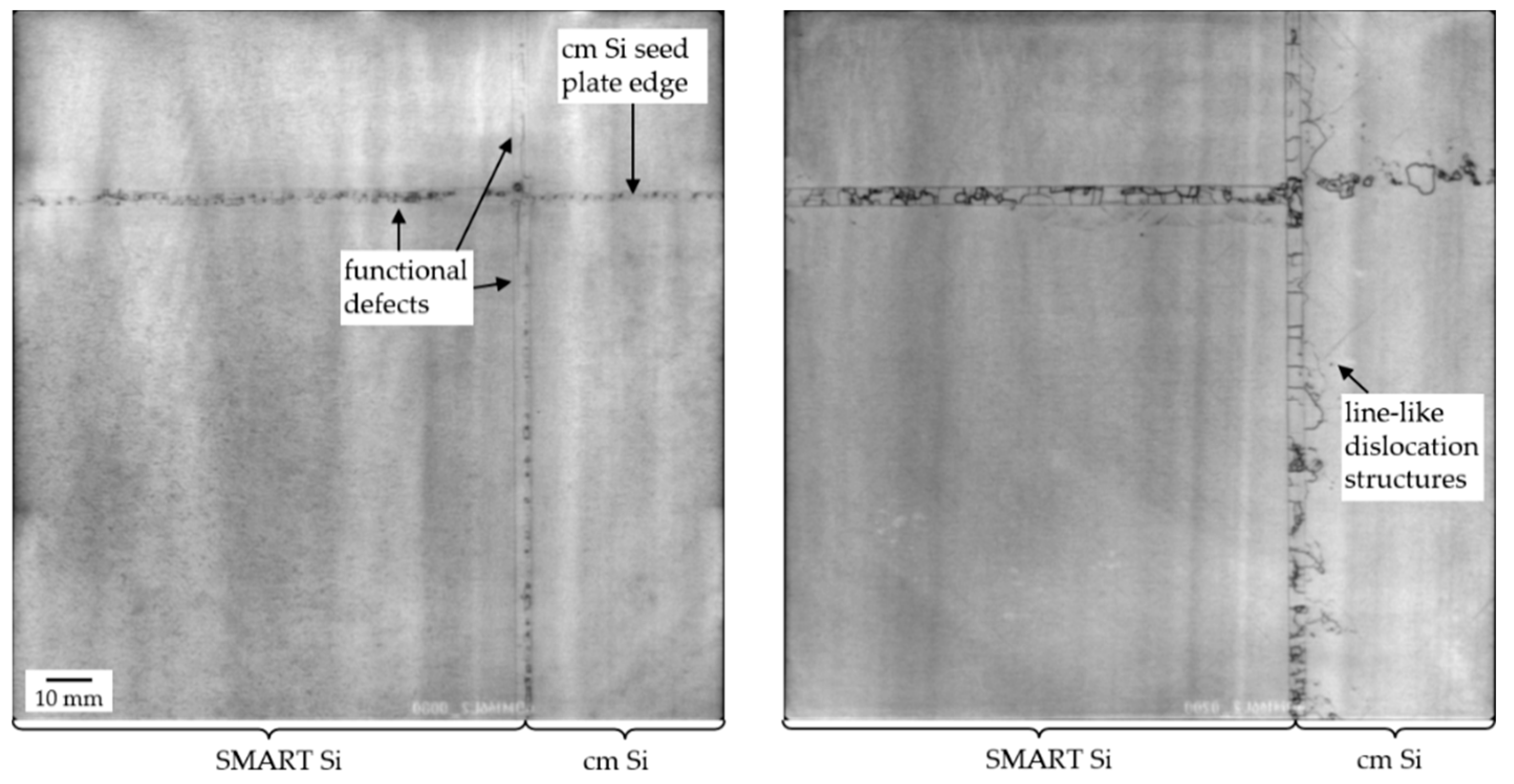
Parasitic grains nucleated on the coating at the crucible wall can be observed to grow towards the intended monocrystalline area. For the classical cm Si approach, these parasitic grains overgrow the <100>-grain induced by the seed plate (see
Figure 2). This overgrowth reduces the monocrystalline area and therefore the efficiency in the resulting solar cell. In case of the SMART Si approach, the functional defects were suitable for the blocking of these parasitic grains (see left side of
Figure 2). This was already reported for smaller sized ingots with an ingot height of 60 mm [
17]. Grains nucleated at the coating of the crucible wall tend to grow into the crystal. The propagation was stopped by the functional defects at the outer edge of the monocrystalline area. Hence, it was possible to maintain the monocrystalline area nearly constant over the whole ingot height.
The monocrystalline area share was estimated in upper brick part via the grain geometry measurements. The analyzed wafer area has a size of 125 mm × 125 mm and is located 20 mm away from the ingot edge. The phase boundary in this ingot part was flat till slightly convex. The segmented grain structure is depicted
Figure 3 for exemplary wafers at three different ingot heights. The mono area is defined via the size of the seeded grain, the white grain in the images. The mono area for the cm Si was reduced down to 50% due to parasitic grains, see
Table 1 The mono area share for cm Si shrinks with increasing brick height as expected, except for the last part, which is due to the determination of the mono share. A double twin boundary can result in two grains with the same grain orientation separated by a twin grain. If this twin grain is very narrow, it will not be detected by the measurement and the algorithm will calculate both grains with same orientation as one grain and thus overestimate the mono area. The mono area for the SMART approach features a nearly constant, higher level over 90% as the blocking of parasitic grains by the functional defects was successful.
3.2. Dislocation Confinement in Functional Defects
Besides ingrowing grain boundaries causing the reduction of the monocrystalline area, dislocation clusters are a big issue reducing the material quality. The analyzed material is located in the center of the ingot with a minimum distance to the ingot edge of 90 mm. The material growing from the contact between the two monocrystalline seed plates on the cm Si half of the ingot shows strong recombination active structures (see each right side of the PL images in
Figure 4). The dislocations arising from a small angular mismatch between the seed plates, due to processing reasons, align to dislocation loops and clusters elongating in lateral direction and thus limiting the material quality with increasing ingot height.
As expected using the SMART approach, the contact between the Si slices with the same orientation induces dislocation structures in the functional defects, as well. In contrast to the cm Si material, the dislocations are confined between the functional grain boundaries forming the functional defect region (see
Figure 4).
With increasing ingot height, line-like recombination active structures emerge on the cm Si half of the ingot with the origin close to the functional defect region (see
Figure 4, right). These line-like structures are most probably dislocations on glide planes. Further microscopic investigations are needed to specify the type of defect. µPL maps of passivated samples enable a more detailed analysis of the functional defect region. The recombination active functional defects can be identified as dislocations loops surrounded by straight grain boundaries (see
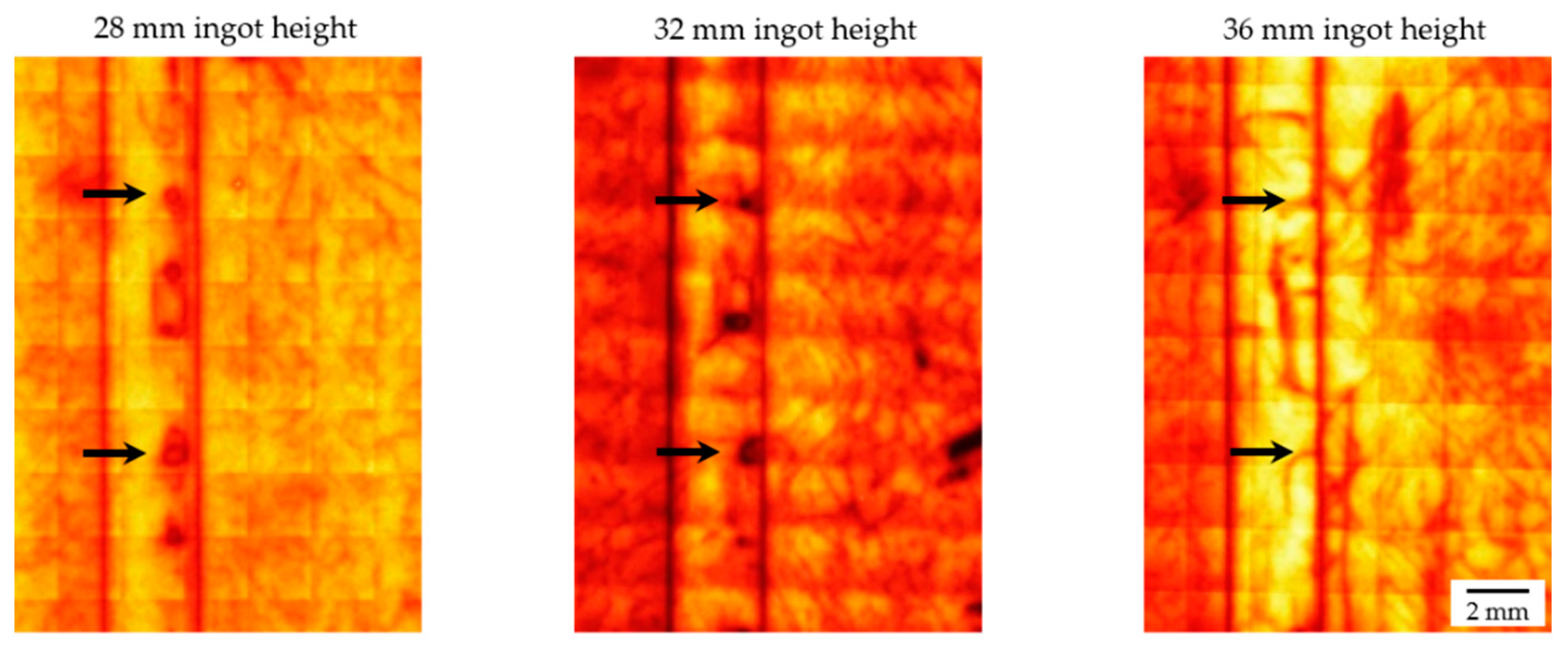
Figure 5). The straight grain boundaries were induced by the orientation difference between the Si plate and Si slices. EBSD measurements confirm a 45° tilt grain boundary. The confined dislocation loops between the functional grain boundaries have no fixed position during the crystallization. Nevertheless, they stay relatively stable and do not generate further dislocations between the functional grain boundaries. Dislocation loops developing towards the functional grain boundaries during the crystal growth were observed to introduce dislocation generation in the neighboring monocrystalline area (see
Figure 5). Two of the dislocation loops in the shown area, marked by black arrows, develop towards the right functional grain boundary between ingot height 28 mm and 32 mm. At the ingot height of 36 mm, the dislocation loops are no longer visible, but line-like dislocation structures are detected in the neighboring grain (right side). Hence, the movement and following interaction of the dislocation loops with the functional grain boundary induces dislocation generation in the neighboring grain.
The generation of line-like dislocation structures was only observed in the cm Si half of the crystallized ingot. The movement and subsequent interaction of the dislocation loops seem to happen only towards the cm Si side of the ingot. Whether this unidirectional movement occurs due to differences in the material or due to the crystallization process could not be clarified so far. One conceivable reason regarding the material would be a different stress for the SMART Si and cm Si half caused by the non-optimal stress reduction in the cm Si part. Assuming dislocation clusters to grow perpendicular to the solid-liquid interface, a in this region of the crystal non-symmetric, convex solid-liquid interface, lowered towards the cm Si half of the ingot, would be a possible explanation regarding the crystallization process. As explained in
Section 2.1, the solid-liquid interface is planar till slightly convex and symmetric as estimated by Eddy current measurements. However, this method is not suitable to detect small irregularities in the form of the solid-liquid interface, which could be decisive in this case with a more or less flat solid-liquid interface. Further experiments investigating stress and the solid–liquid interface in a microscopic scale and enabling statistics due to a larger variety of samples are necessary.
3.3. Cellular Structures in Monocrystalline Area
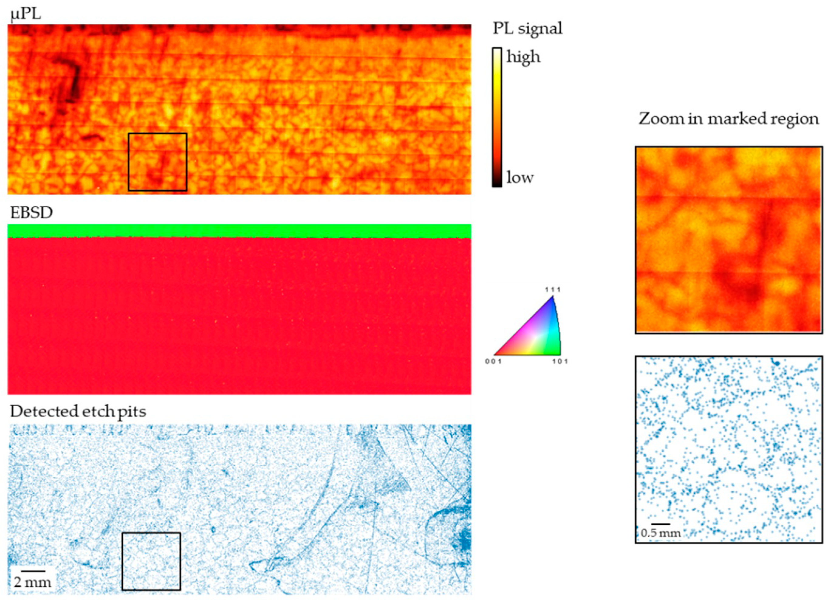
While the monocrystalline area surrounded by the functional defects shows a relatively uniform PL signal in the as cut condition promising a homogeneous monocrystalline material, recombination active cellular structures in the monocrystalline area of the lower ingot height are visible via µPL of passivated samples (see
Figure 6, top). These cellular structures are less recombination active than the dislocation loops in the functional defects, visible at the upper edge of this µPL map, but spread all over the monocrystalline area in the lower ingot part. With increasing ingot height, these cellular patterns increase in diameter, but structures are less recognizable and at an ingot height of 100 mm not visible anymore. Whether the underlying defect disappears or the recombination activity is reduced is not yet clarified.
EBSD measurements were performed in this area to investigate the underlying defect for the cellular structures. The induced 45° tilt grain boundary could be verified and the material grown above the monocrystalline seed plate turned out to be really monocrystalline (see
Figure 6, middle). No cellular structures could be detected with the EBSD system with an angular resolution of 0.3°.
In microscope images of polished and subsequently Cr-less etched samples at the same position, etch pits with some cellular pattern could be detected (see
Figure 6, bottom). Therefore, these cellular recombination active clusters are regarded at dislocation clusters with a distinct cellular pattern in conjunction with a lower recombination activity in comparison to the aforementioned dislocation tangles. The dislocation density detected via etch pits in the monocrystalline area, as exemplarily shown in
Figure 6, bottom, is 7 × 10
3 cm
−2, which is up to two magnitudes lower than in other cast-mono Si reported in literature with values from 1 × 10
4 cm
−2 to 6 × 10
5 cm
−2 [
7,
18]. The comparison of the PL signal and the detected etch pits in a magnified region of the same area (
Figure 6, right) shows that etch pits seem to align and these lines of higher dislocation density are roughly corresponding to the low PL signal regions. This alignment of dislocations to a cellular pattern was already observed by Oliveira et al. [
19,
20] and Krause et al. [
20]. The size of the cellular patterns is comparable to that reported in the literature, albeit the density of etch pits is lower in our case. Oliveira et al. [
19] and Krause et al. [
20] observed the cellular pattern perpendicular to the growth direction, the patterns shown here were observed parallel to the growth direction. In combination, this means that the three-dimensional geometry of these patterns is a bubble, rather than a column. This explains the observation that the aligned etch pits do not exactly fit the low PL signal regions because the measurement was performed on parallel wafers and thus the specific geometry of the dislocation structure might have changed between those two. However, the cellular pattern with low PL signal could be attributed to a cellular dislocation pattern in the monocrystalline area.
3.4. Summary
The SMART approach worked well for the blocking of parasitic grains. The monocrystalline area was kept almost constant over 90% for the whole ingot height. This enables a high material quality and potential for solar cells due to nearly no recombination active grain boundaries and the possibility to use the effective texturing process for monocrystalline material.
As expected, dislocations structures built between the functional grain boundaries. The confinement of these dislocations was almost successful for most parts. Dislocation structures developing towards functional grain boundaries induced new line-like defects in the mono area next to the functional defect. As a possible further improvement, a more stable phase boundary would decelerate the lateral movement of the dislocation structures and thus inhibit the nucleation of new dislocations in the neighboring grain. Another possibility could be the use of a second functional grain boundary surrounding the functional defect region. This could impede the propagation of the dislocation structures as they are additionally blocked by the second large angle grain boundary. Moreover, parasitic grains nucleated at the crucible wall could be blocked even more effectively.
Although dislocations could be confined in the functional defect region, a dislocation density of 7 × 103 cm−2 was detected in the monocrystalline area. The dislocations aligned in a cellular pattern reduce the lifetime and thus are visible as low PL signal regions for low ingot heights. Dislocations multiply and rearrange due to thermo-mechanical stress. Therefore, a modification of the crystallization process in combination with SMART Si approach is needed for a further reduction of the dislocation density and the resulting recombination activity.
4. Evaluation of Material Quality and Solar Cell Efficiency
To compare the material quality, high-performance multicrystalline (hp mc) Si material with fine crystal grains crystallized with a similar set-up and thermal recipe was processed in the same high-temperature batch as the cm Si and SMART Si material discussed in this paper. The materials crystallized with cm Si and SMART approach feature more homogeneous and higher average effective lifetimes than the hp mc Si material (see
Figure 7). However, it should be noted that the hp mc Si material features a lower resistivity partly responsible for increased recombination. Nevertheless, this comparison shows the efficient suppression of strongly recombination active structural crystal defects by the cm Si and especially the SMART approach.
Obviously, all three materials show a difference in recombination active structural defects reducing the lifetime as expected. While the amount of grain boundaries and dislocations is strongly decreased from hp mc Si to cm Si, the SMART Si material shows even less. A large fraction of the lifetime deterioration in the cm Si and SMART Si is not due to the material but rather process-related artefacts like the area of reduced lifetime at the lower (cm Si), respectively upper edge (SMART Si). Highest effective lifetime values at 1/20 suns are around 1200 µs for all three materials in the inner grain and mono area. The influence of the structural defects is very pronounced at the depicted measurement at 1/20 suns, which illustrates the injection condition of a final solar cell at 1 sun at the maximum power point. This minimized lifetime reduction at working conditions is a further advantage of the SMART Si material.
Due to the promising material quality of the SMART Si, this material was used as the base material of a TOPCon solar cell [
15]. A sample from the previously shown ingot height of 130 mm and a resistivity of 0.9 Ωcm obtained the certified record efficiency of 23.3% (V
oc = 699 mV, J
sc = 40.9 mA/cm
2, FF = 81.5%) [
21]. The sample was textured with random pyramids and was processed with a double layer anti-reflection coating.
5. Conclusions
The SMART approach was successfully transferred to a G2-sized silicon ingot enabling better material quality than the standard cm Si. The blocking of parasitic grains was effective in such a way that the monocrystalline area could be held higher than 90% all over the ingot height, which is a big improvement compared to the cm Si with a mono area declining to 50%. In addition, an improved control of the other crystal defect, dislocations, was reported. The confinement of dislocations in the functional defects was relatively stable but has still room for future improvement, where different compositions of the functional defects could be evaluated. A recombination active cellular structure was observed in the monocrystalline area which could be correlated with the dislocation distribution even if the dislocation density is low. It could not be clarified yet if these cellular structures limit the material quality for solar cells. Lifetime measurements after a typical high temperature process chain would be useful for this evaluation. The comparison of the material quality of SMART Si, cm Si, and hp mc Si at 130 mm showed a clear benefit of the SMART Si material due to its high homogeneity and low defect density. This SMART Si material was processed as a TOPCon solar cell and obtained a certified record efficiency of 23.3%.
Author Contributions
Conceptualization, P.K., Y.H., S.R. and N.U.; software, T.T.; investigation, P.K., T.T. and F.S.; writing—original draft preparation, P.K.; writing—review and editing, F.S., T.T., S.R. and N.U. All authors have read and agreed to the published version of the manuscript.
Funding
This work was partially supported by the German Federal Ministry for the Economy and Energy, grant number 0325491 and 0324034, and Japan Science and Technology Agency, grant number JPMJCR17J1.
Institutional Review Board Statement
Not applicable.
Informed Consent Statement
Not applicable.
Data Availability Statement
Not applicable.
Acknowledgments
The authors would like to thank Wacker Polysilicon for the silicon materials and express their gratitude to the crystallization, cell processing and characterization teams at Fraunhofer ISE, Fraunhofer THM, and Nagoya University for their support and input in many valuable discussions.
Conflicts of Interest
The authors declare no conflict of interest. The funders had no role in the design of the study; in the collection, analyses, or interpretation of data; in the writing of the manuscript, or in the decision to publish the results.
References
- Pujari, N.S.; Cellere, G.; Falcon, T.; Zwegers, M.; Bernreuter, J.; Haase, J.; Coletti, G.; Romijn, I.; Kroon, J.; Geerlings, B.; et al. International Technology Roadmap for Photovoltaic (ITRPV). 2018. Available online: http://www.itrpv.net/ (accessed on 23 July 2018).
- Stoddard, N.G.; Wu, B.; Witting, I.; Wagener, M.C.; Park, Y.; Rozgonyi, G.A.; Clark, R.F. Casting Single Crystal Silicon: Novel Defect Profiles from BP Solar’s Mono^2 TM Wafers. Solid State Phen. 2008, 131–133, 1–8. [Google Scholar] [CrossRef]
- Hu, D.; Zhang, T.; He, L.; Chen, H.; Zhong, D.; Cao, S.; Gao, J.; Wan, Y. The characteristics of sub-grains in the mono-like silicon crystals grown with directional solidification method. In Proceedings of the 38th IEEE Photovoltaic Specialists Conference, Austin, TX, USA, 3–8 June 2012; pp. 2735–2738. [Google Scholar]
- Kaden, T.; Petter, K.; Bakowskie, R.; Ludwig, Y.; Lantzsch, R.; Raschke, D.; Rupp, S.; Spiess, T. Analysis of Mono-cast Silicon Wafers and Solar Cells on Industrial Scale. Energy Procedia 2012, 27, 103–108. [Google Scholar] [CrossRef] [Green Version]
- de Oliveira, V.A.; Tsoutsouva, M.; Lafford, T.; Pihan, E.; Barou, F.; Cayron, C.; Camel, D. Sub-grain boundaries sources and effects in large mono-like silicon ingots for PV. In Proceedings of the 29th European Photovoltaic Solar Energy Conference and Exhibition, Amsterdam, The Netherlands, 22–26 September 2014. [Google Scholar] [CrossRef]
- Gong, L.; Wang, F.; Cai, Q.; You, D.; Dai, B. Characterization of defects in mono-like silicon wafers and their effects on solar cell efficiency. Sol. Energy Mater. Sol. Cells 2014, 120, 289–294. [Google Scholar] [CrossRef]
- Gu, X.; Yu, X.; Guo, K.; Chen, L.; Wang, D.; Yang, D. Seed-assisted cast quasi-single crystalline silicon for photovoltaic application: Towards high efficiency and low cost silicon solar cells. Sol. Energy Mater. Sol. Cells 2012, 101, 95–101. [Google Scholar] [CrossRef]
- Kutsukake, K.; Usami, N.; Ohno, Y.; Tokumoto, Y.; Yonenaga, I. Control of Grain Boundary Propagation in Mono-Like Si: Utilization of Functional Grain Boundaries. Appl. Phys. Express 2013, 6, 25505. [Google Scholar] [CrossRef]
- Takahashi, I.; Joonwichien, S.; Iwata, T.; Usami, N. Seed manipulation for artificially controlled defect technique in new growth method for quasi-monocrystalline Si ingot based on casting. Appl. Phys. Express 2015, 8, 105501. [Google Scholar] [CrossRef]
- Bean, C.P.; DeBlois, R.W.; Nesbitt, L.B. Eddy-current method for measuring the resistivity of metals. J. Appl. Phys. 1959, 30, 1976–1980. [Google Scholar] [CrossRef]
- Strauch, T.; Demant, M.; Krenckel, P.; Riepe, S.; Rein, S. Identification of Defect-Supressing Grain Boundaries in Multicrystalline Silicon Based on Measurements of As-Cut Wafers Using Advanced Image Processing. In Proceedings of the 33rd European Photovoltaic Solar Energy Conference and Exhibition, Amsterdam, The Netherlands, 25–29 September 2017; pp. 313–317. [Google Scholar] [CrossRef]
- Strauch, T.; Demant, M.; Krenckel, P.; Riepe, S.; Rein, S. Analysis of grain structure evolution based on optical measurements of mc Si wafers. J. Cryst. Growth 2016, 454, 147–155. [Google Scholar] [CrossRef]
- Abbadie, A. Chromium-Free Etching Solution for Si-Substrates and Uses Therefor. U.S. Patent 7,635,670, 22 December 2009. [Google Scholar]
- Takato, H.; Sakata, I.; Shimokawa, R. Quinhydrone/Methanol Treatment for the Measurement of Carrier Lifetime in Silicon Substrates. Jpn. J. Appl. Phys. 2002, 41, L870–L872. [Google Scholar] [CrossRef]
- Feldmann, F.; Bivour, M.; Reichel, C.; Steinkemper, H.; Hermle, M.; Glunz, S.W. Tunnel oxide passivated contacts as an alternative to partial rear contacts. Sol. Energy Mater. Sol. Cells 2014, 131, 46–50. [Google Scholar] [CrossRef]
- Giesecke, J.; Schubert, M.C.; Michl, B.; Schindler, F.; Warta, W. Minority carrier lifetime imaging of silicon wafers calibrated by quasi-steady-state photoluminescence. Sol. Energy Mater. Sol. Cells 2011, 95, 1011–1018. [Google Scholar] [CrossRef]
- Kutsukake, K.; Usami, N.; Ohno, Y.; Tokumoto, Y.; Yonenaga, I. Mono-Like Silicon Growth Using Functional Grain Boundaries to Limit Area of Multicrystalline Grains. IEEE J. Photovolt. 2014, 4, 84–87. [Google Scholar] [CrossRef]
- Miyamura, Y.; Harada, H.; Jiptner, K.; Chen, J.; Prakash, R.R.; Nakano, S.; Gao, B.; Kakimoto, K.; Sekiguchi, T. Crystal growth of 50 cm square mono-like Si by directional solidification and its characterization. J. Cryst. Growth 2014, 401, 133–136. [Google Scholar] [CrossRef]
- Oliveira, V.A.; Rocha, M.; Lantreibecq, A.; Tsoutsouva, M.G.; Tran-Thi, T.N.; Baruchel, J.; Camel, D. Cellular dislocations patterns in monolike silicon: Influence of stress, time under stress and impurity doping. J. Cryst. Growth 2018, 489, 42–50. [Google Scholar] [CrossRef]
- Krause, A.; Sylla, L.; Oriwol, D. Plastic Deformation as an Origin of Dislocations in Cast Mono. Energy Procedia 2016, 92, 833–838. [Google Scholar] [CrossRef] [Green Version]
- Schubert, M.C.; Schindler, F.; Benick, J.; Riepe, S.; Krenckel, P.; Richter, A.; Müller, R.; Hammann, B.; Nold, S. The potential of cast silicon. Sol. Energy Mater. Sol. Cells 2021, 219, 110789. [Google Scholar] [CrossRef]
| Publisher’s Note: MDPI stays neutral with regard to jurisdictional claims in published maps and institutional affiliations. |
© 2021 by the authors. Licensee MDPI, Basel, Switzerland. This article is an open access article distributed under the terms and conditions of the Creative Commons Attribution (CC BY) license (http://creativecommons.org/licenses/by/4.0/).

 ,
, 


