Article

Cadmium Telluride Nanocomposite Films Formation from Thermal Decomposition of Cadmium Carboxylate Precursor and Their Photoluminescence Shift from Green to Red

Fusion and Technologies for Nuclear Safety and Security Department, Physical Technologies for Safety and Health Division, Photonics Micro and Nanostructures Laboratory, ENEA C.R. Frascati, via E. Fermi 45, 00044 Frascati (RM), Italy
*
Author to whom correspondence should be addressed.
Submission received: 5 February 2021 / Revised: 24 February 2021 / Accepted: 25 February 2021 / Published: 3 March 2021

Abstract

:
This study focuses on the investigation of a CdTe quantum dots (QDs) formation from a cadmium-carboxylate precursor, such as cadmium isostearate (Cd(ISA)2), to produce CdTe QDs with tunable photoluminescent (PL) properties. The CdTe QDs are obtained by the thermal decomposition of precursors directly in the polymer matrix (in situ method) or in solution and then encapsulated in the polymer matrix (ex situ method). In both approaches, the time course of the CdTe QDs formation is followed by means of optical absorption and PL spectroscopies focusing on viable emission in the spectral interval between 520 and 630 nm. In the polymeric matrix, the QDs formation is slower than in solution and the PL bands have a higher full width at half maximum (FWHM). These results can be explained on the basis of the limited mobility of atoms and QDs in a solid matrix with respect to the solution, inducing an inhomogeneous growth and the presence of surface defects. These achievements open the way to the exploitation of Cd(ISA)2 as suitable precursor for direct laser patterning (DPL) for the manufacturing of optoelectronic devices.

1. Introduction

The interest in the semiconductor quantum dots (QDs) stems from their unique optical and electronic properties compared to bulk materials [1]. Indeed, as a consequence of the quantum confinement effect, the band gap of semiconductor QDs can be tuned with the size and shape of the particles [2]. The intensive studies on these materials showed also the possibility to reach photoluminescence quantum yields (PLQY) above 70%, color saturation related to narrow photoluminescence (PL) linewidth (full width at half maximum, FWHM, between 20 and 40 nm), and precisely tunable emission wavelengths based on the control of composition and size [3,4,5]. All these developments were possible, because during the last decades the synthetic strategies of semiconductor QDs allowed the precise control of size, size distribution shape and composition. In general, the semiconductor QDs are formed with IV, II-VI, I-III-VI, I-II-IV-VI grouped material and among them the II-VI cadmium-chalcogenide compounds show excellent optical properties and can be incorporated into polymer matrices [6].
The possibility to incorporate the cadmium-chalcogenide QDs within the polymeric matrices further stimulate the interest toward industrial photonics application such as for solar concentrators [7], waveguides [8], biological labels [9] and light emitting diodes (LED) [10,11]. In general, the nanocomposite can be obtained by mixing the preformed QDs and polymer (ex situ methodology) or inducing the growth of the QDs within the pre-formed polymer (in situ methodology). In this last case the semiconductor QDs formation is achieved by the transformation of a suitable precursor induced by a chemical reaction [12] or by an energy variation (temperature or radiation) [13,14,15,16].
The formation of the cadmium-chalcogenide QDs when activated by an external source of energy in the form of heat or radiation is of particular interest, because it can be localized allowing the patterning of the semiconductor QDs. Recently this basic idea has been shown possible by several authors and it is the basis of the direct laser patterning approach, i.e., the process in which the laser source modifies a material to obtain the desired effect (QDs formation) [17] only in specific area of the sample (patterning) [18,19]. To date, the work showed in these papers is focused mainly on the formation of CdS QDs from the cadmium bis(benzythiolate) precursor [20] and only recently of the CdSe QDs from cadmium 2-(N,N-dimethylamino)ethylselenolate [21,22]. In all these cases, the PL emission obtained with the laser process is broad (from 400 to 600 nm) and the possibility of modulating the PL emission tuning the laser parameters it is not well defined.
To overcome this limitation, in this study the synthesis of a new type of precursor generating the CdTe QDs by thermal treatment within a polymer is reported together with the possibility to produce CdTe QDs with a PL band from green to red. The selection of this cadmium chalcogenide compound is due to its band-gap properties. Indeed, CdTe QDs have has a narrow band-gap of 1.5 eV [23], which is suitable for producing QDs absorbing and emitting at visible-near infrared (NIR) wavelengths by modulating the nanometric size of the particles within a small range (2–5 nm) [2,24]. Regarding the possibility of having a precursor with a PL emission ranging from green to red, changing the annealing time would be the preliminary step to test this precursor for laser patterning of the QDs.
Several precursors are reported to prepare II-VI QDs [25], and in recent literature, some of the most used precursors of CdS and CdSe QDs in solid state are mainly single source precursors like cadmium thiolates [26,27], cadmium xanthates [13,28] and cadmium selenolate [29]. These compounds show three main characteristics: (i) high solubility in organic solvent (ii) a decomposition temperature below 300 °C degrees and (iii) a relatively simple way of synthesis [30].
Although all this work has been done using CdS and CdSe precursors, little is reported regarding the synthesis of CdTe nanocrystals from single source precursors in thin films. A well identified and studied CdTe QDs single source precursor is the cadmium ligand of the ditelluride(imidodiphosphinate) as reported in ref [31]. However, the synthesis of such a compound requests several steps and many of them need to be followed under controlled atmosphere and request careful sample handling and specific analysis. In this case a simpler chemical approach may guarantee the QDs synthesis and also the industrial application of the process.
The complex chemical path pushed the research toward a simpler strategy of nano-composite synthesis involving the dual source precursors [32,33,34] in which the sources of cadmium and of tellurium are located in two different molecules that are finally mixed with the polymer.
In this context, the novelty of this work is to find the suitable precursors and the physical conditions for the formation of CdTe QDs within a polymer to promote their in situ growth with photoluminescent (PL) emission ranging from green to red of the visible spectrum. The majority of the literature reported the ex situ formation of the CdTe nanocomposites [35], and only few references reported the in situ generation of CdTe QDs but not in film [33]. In this work, the CdTe QDs are formed in the solid state, i.e., in a polymer/precursor film that is annealed after its deposition.
For this purpose, the film chemical composition and the CdTe QDs growth conditions have to be carefully studied. In particular a key step is the choice of cadmium and chalcogenide precursors that should have a relatively low decomposition temperature and high solubility in hydrophobic polymers to be applied on devices [10]. Then it is important to investigate the conditions of QDs growth, such as temperature and reaction time, suitable to produce CdTe QDs with PL emission ranging from green to red. In this perspective, a carboxylate complex of cadmium, namely the cadmium isostearate (Cd(ISA)2) and the tri-n-octyl phosphine telluride (TOP-Te), were selected as metal and chalcogenide sources for CdTe QDs.
The CdTe QDs obtained directly in the polymer matrix (in situ method) through the thermal decomposition of the precursors were analyzed by means of UV-Vis absorption and PL spectroscopies, transmission electron microscopy (TEM), and scanning transmission electron microscopy (STEM). A further study of the nanocomposite film was made by forming the CdTe nanocomposite film through mixing the polymer with CdTe QDs prepared in solution (ex situ methodology).

2. Materials and Methods

2.1. Chemicals

Cadmium oxide (CdO, 99.5%), tellurium (Te, 99.8%), trioctylphosphine (TOP), poly(methyl methacrylate) (PMMA), isostearic acid (ISA, technical grade, 90%), octadecene (ODE technical grade, 90%), and chloroform (≥99.8%) were purchased from Sigma-Aldrich (Milano, Italy) and used without further purification.

2.2. Synthesis of Cadmium Isostearate (Cd(ISA)2)

The synthesis of cadmium isostearate (Cd(ISA)2) is carried out according to the procedure reported in literature with minor modifications for the cadmium carboxylate compounds [35].
In a 25 mL three-bottom flask, 2.6 mL of ISA (8 mmol), 7.5 mL of ODE (23.4 mmol), and 385 mg (3 mmol) of CdO are mixed. The mixture is degassed at 100 °C for 20 min and exposed under nitrogen for 15 min. After that, the temperature is raised at 280 °C to better dissolve the CdO under nitrogen gas. The system is kept at 280 °C for a further 30 min to allow for the formation of Cd(ISA)2, obtaining a final colorless homogeneous solution. After this period, the system is cooled down at room temperature, and the crude of reaction is washed by adding acetone to eliminate the excess of ISA to give compound Cd(ISA)2 (4.8 g, 7 mmol, 87.5%).
In order to confirm the structure of Cd(ISA)2 compound, a high-resolution 1H-NMR-spectra is acquired by using a Bruker AM-400 instrument. The chemical shifts of the analyzed structure are referenced to the residual peaks of the deuterated solvent: chloroform (7.26 ppm). The results of the analysis are reported below.
The 1H-NMR spectrum of Cd(ISA)2 (400 MHz, 20 °C, CDCl3, m = multiplet and br, m = broad multiplet), δ (ppm): 2.4–2.36 (m, 4H,-CH2-CO2-), 1.32–1.15 (m, 58H, 2x -CH-(CH2)14-), 0.95–0.89 (br, m, 12H, 4x -CH3) ppm, confirms the identity of chemical compound.

2.3. Synthesis of CdTe QDs Films via In Situ Route

The hybrid polymeric films containing cadmium and tellurium precursors are prepared as following.
First of all, polymer solution is prepared dissolving the PMMA into chloroform to achieve final concentrations of 200 mg/mL. In a vial, 1 mL of the polymeric solution and 40 mg (0.059 mmol) of Cd(ISA)2 are mixed. The mixture is left under stirring for 1 h at T = 35–40 °C until Cd(ISA)2 is completely dissolved. Within the Glove Box (ITECO G50), 16.5 μL of trioctylphosphine telluride (TOP-Te) solution 0.9 M [36] are added to the preparation, respecting the mol ratio of Cd and Te to 4:1 [34]. The mixture is taken out of the Glove Box and left again stirring for 1 h at T = 35–40 °C to achieve a completely homogeneous solution.
The solution is used to produce films by the spin-coating technique on quartz slides (20 × 10 mm2) for optical characterization. The depositions are performed by using a PoloSpin 150i/200i spin coater. The films are produced on substrates by dropping 80 μL of the solution and by spinning for 45 s at 1000 rpm with a max recipe speed of 1000 rpm. To generate the CdTe QDs within the polymeric matrix the films are annealed under vacuum by means of a Buchi furnace B585. The temperature and the time of annealing are investigated in the range between 120–180 °C and 5–120 min, respectively. The samples are repeated three times to test the reproducibility of the procedure.

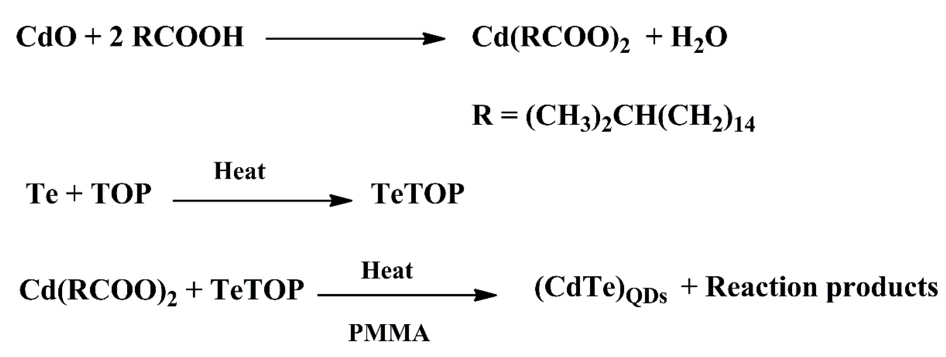
2.4. Synthesis of CdTe QDs via Ex Situ Route

In a three-neck round-bottom flask, 20 mL of ODE are exposed to vacuum for 20 min at 100 °C. After that, 200 mg (0.3 mmol) of Cd(ISA)2 are added to the solution and the mixture is left stirring under nitrogen at 100 °C for 1 h to dissolve the Cd(ISA)2 completely. Subsequently, the mixture is cooled down at room temperature, divided into rates of 2 mL, and 8 µL of trioctylphosphine telluride (TOP-Te) solution 0.9 M are added in each solution under inert condition within the Glove Box, respecting the mol ratio of Cd and Te to 4:1.
Each solution is taken out of the Glove Box and left again stirring at 150 °C for different periods of time, 5, 10, 15, 20, 30, and 60 min respectively, to obtain CdTe nanocrystals with different morphological and photophysical features. After each period, the tubes with the solutions are removed from the hotplate and cooled down to room temperature in water.
To precipitate the CdTe QDs from ODE a volume of 2 mL from each tube is divided into ten Eppendorf.tubes A volume of 1.5 mL of acetone is added to 200 µL of CdTe QDs solution in the Eppendorf tube and centrifuged at 15,000 rpm for 10 min. Subsequently, the supernatant is discarded and the precipitate is collected and dissolved in toluene.
In addition, in this case, the samples are repeated three times to test the reproducibility of the methodology.

2.5. Synthesis of CdTe QDs Encapsulated in Polymeric Films via Ex Situ Route

In order to encapsulate the CdTe QDs produced by the ex-situ method in an appropriate polymer matrix, 200 µL of a 200 mg/mL solution of PMMA are added to CdTe QDs dried under nitrogen gas. The final solution is stirred at room temperature for 10 min and used to produce films by the spin-coating technique on quartz slides (20 × 10 mm2) for optical characterization. The depositions are performed by using a PoloSpin 150i/200i spin coater. The films are produced on substrates by dropping 80 μL of the solution and by spinning for 45 s at 1000 rpm with a max recipe speed of 1000 rpm.

2.6. Characterizations

The optical properties of the samples are investigated by UV-Vis absorption and PL spectroscopies measurements.
Absorption spectra are recorded on a Jasco V750 spectrophotometer (Jasco Europe–Cremella (Lc), Italy), in a spectral range of 200–800 nm, the integration time of 0.6 s, and slit widths of 1.5 nm.
PL emission spectra are obtained by using a Fluoromax 4 Plus (Horiba Italia s.r.l. Roma Italy) spectrofluorometer equipped with Origin program for data acquisition and analysis in the spectral range from 450 to 690 nm. The excitation wavelength of 350 nm is used with a spectral bandwidth of 1.5 nm for both the excitations and emission monochromators and a cut off filter at 399 nm to characterize all the samples. The curves are automatically corrected for the spectral response of the detector.
UV-Vis absorption and PL emission spectra of CdTe QDs obtained with solvothermal synthesis are recorded using toluene as solvent.
The morphological and structural properties of the samples are investigated by TEM and HAADF-STEM analyses (the microscope and all the TEM accessories listed below are from Thermo Fisher Scientific-Milano). The TEM analyses are performed with a FEI TECNAI F20 microscope operating at 200 keV. The instrument is also equipped with a dispersion micro-analysis of energy (EDS) and the STEM accessory. The TEM images are taken in the phase contrast mode (HREM).
The STEM pictures are recorded using a High Angle Annular Dark Field (HAADF) detectors: in this imaging mode, the intensity I is proportional to Z1.7t, where Z is the mean atomic number and t is the thickness of the specimen.
Before the TEM observation, the CdTe QDs films are dissolved in 500 μL chloroform to obtain a final solution that is dropped over a TEM grid for the next observation.
The TEM analysis of the CdTe QDs obtained with solvothermal synthesis was carried out by diluting the prepared solution to obtain a monolayer of nanoparticles visible on the TEM grid.

2.7. Data Analysis

All the PL and UV-Vis spectra are elaborated with Origin Pro program.
The averaged particle size (d) is estimated from the UV-Vis spectra according to the empirical equation (Equation (1)) derived as shown Equation (1)) derived as shown by Kamal et al. [37]:
E g ( d )   =   1.51 +   1 0.048 d 2 + 0.29 d 0.09
where Eg(d) is the band-gap energy of the QDs in eV that is determined from the wavelength of the first exciton peak in the absorption spectrum and “d” is the QDs diameter expressed in nm.
The PL spectra are normalized to 1 and deconvolved by using Gaussian functions to determine the peak position, amplitude (FWHM) and integrated intensity of the bands.
The error bars are estimated in term of standard deviation over three set of experiments.

3. Results and Discussion

3.1. CdTe QDs Films via In Situ Route

In order to form a homogeneous mixture of cadmium, tellurium, and PMMA that will ensure a QDs uniform distribution, both precursors have to be soluble in organic solvents. The cadmium atom becomes soluble in organic solvent when it is bound with a fatty acid to form a cadmium carboxylate [38]. In the present case, the cadmium carboxylate has been obtained by combining the cadmium oxide with isostearic acid in the presence of a solvent (ODE) at relatively high temperature. On the other side the Te solubilization has been obtained, dissolving the Te in TOP with a TOP/Te molar ratio slightly more than 2. The TOP-Te liquid is soluble in chloroform, so the PMMA can be readily added to the solution. In such a way, the precursors and the polymer are ready to be mixed to form a thin film. The film contains all the reagents that under thermal treatment can react to give the expected product CdTe QDs following Scheme 1 [39].
In order to find the conditions of the CdTe QDs formation with an emission spanning from green to red wavelengths, the effect of the annealing temperature and time is explored. In particular, the goal of this first set of the experiment is to determine a relatively low temperature (below 200 °C in order to preserve the polymer from decomposition) that induces the CdTe QDs formation according to Scheme 1. Then, it is necessary to find an appropriate time interval that allows the formation of QDs of variable size, i.e., optical properties.

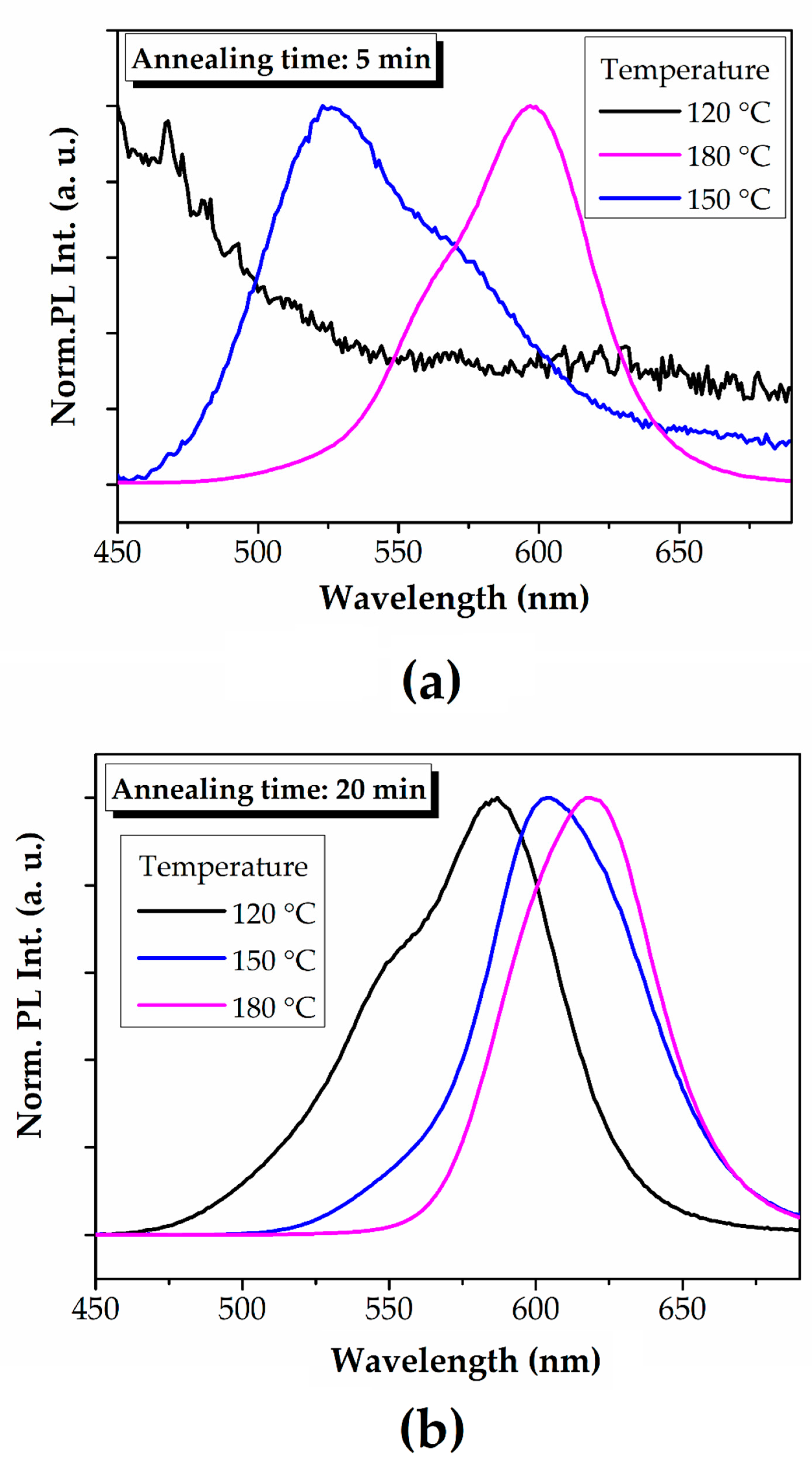
3.1.1. Effects of the Annealing Temperature

In the first set of experiments, the reaction conditions to grow CdTe nanocrystals with tunable emission properties are estimated by investigating the effects produced by the temperature in the range from 120 to 180 °C and by the time for 5 and 20 min.
In Figure 1, the normalized PL spectra of the films prepared in different conditions of time and temperature are reported. Figure 1a shows the PL emission spectra of three films annealed at different temperatures (120, 150, and 180 °C) for 5 min. On the basis of a previous studies [33,34] and by considering the reactivity of the CdTe QDs from Cd(ISA)2 and TOP-Te precursors, the PL signals can be reasonably ascribed to the formation of CdTe nanocrystals. It is evident that an annealing process of 5 min at 120 °C does not produce any PL emission (black line), suggesting the non-formation of luminescent CdTe nanocrystals. In contrast, the increase of the temperature to 150 °C (blue line) produces a PL emission centered at 525 nm with a shoulder at 570 nm, suggesting the presence of two groups of CdTe nanocrystals. The further increase in temperature to 180 °C for 5 min produces an emission band with a peak at 598 nm (purple line) and a shoulder at 560 nm, pointing out that two populations of QDs still exist, but the main products are the red QDs.
Figure 1b shows the PL emission spectra for three films annealed at different temperature (120, 150, and 180 °C) for a longer time of 20 min. As a general trend, one can see that the increasing in the duration of the annealing process from 5 to 20 min produces a red shift of the peak wavelength.
The PL emission spectrum of the film annealed at 120 °C for 20 min (black line) shows a principal peak at 585 nm with a shoulder at 550 nm, indicating the presence of two populations of CdTe nanocrystals. Considering that the annealing process at 120 °C for 5 min produced no luminescent films, one can rule out such a temperature condition for the synthesis of CdTe QDs.
As regards the films processed at 150 and 180 °C for 20 min (blue and purple lines), the spectra show similar shape and exhibit PL peaks at about 600 and 618 nm, respectively, suggesting the formation of one population of CdTe nanocrystals.
The overall picture of the trend of photoluminescence maxima as a function of the annealing temperature and time is shown in Table 1, and it is used to identify the best conditions to study the growth process of CdTe QDs in the polymeric matrix. To obtain an emission spanning from green to red wavelengths, the temperature of 150 °C is chosen for further experiments on the basis of the greatest distance (∆PL) of the PL maxima at 5 and 20 min.
This temperature is relatively low to allow the formation of the QDs without destroying the polymer or for further application on electrooptical devices.

3.1.2. Effects of the Annealing Time

The second set of experiments is carried out to investigate the time course of the absorption and PL properties, at 150 °C in the hybrid films. Figure 2 reports the images taken under the UV lamp at 365 nm and the respective absorption and normalized PL spectra of the samples annealed for 5, 10, 20, 30, 60, and 120 min under vacuum. It is evident that the duration of the annealing process allows modulating the emission properties (the size of the CdTe QDs) of the films from green to red wavelengths. The absorption spectra of the samples show well distinct absorption maximum, which is reasonably due to the first electronic transition of CdTe QDs. The main absorption peak shifts from 524 to 570 nm, as the duration of the annealing process increases, indicating that the annealing time is crucial to modulate the optical properties of the CdTe nanocrystals grown within the PMMA matrix.
The same trend is observed for the averaged peak position of the PL bands, which move from 551 to 608 nm. Considering that the optical features of QDs are strongly dependent on their size, the averaged dimension (d) of the nanocrystals produced within the polymeric films is estimated from the absorption spectra according to Equation (1).
Table 2 summarizes the value of the QDs size as derived from PL spectral characteristics of the nanocomposites as a function of time.
The trend of the QDs size (d) as a function of the annealing time is reported in Figure 3.
The trend of the estimated average size of the CdTe QDs is described by an exponential growth function meaning that the formation of CdTe QDs occurs relatively fast during the first minutes of the annealing process, producing nanocrystals with a size around 2.82 nm. Then the growth process becomes slower, and the averaged size approaches 3.37 nm. The trend of this curve can be reasonably explained on the basis of the processes occurring for the QDs growth in solution for the reactions between the cadmium carboxylates and phosphine chalcogenides [38,40,41].
As a matter of fact, the general consensus on the formation mechanism of CdE (E = S, Se, Te) QDs in solution is that the cadmium carboxylate and phosphine chalcogenide (TOP-E) starts to react forming a monomer, CdE, that subsequently undergoes crystallization by assembly into nanocrystals [38]. The CdE monomer is formed by the reaction of the cadmium carboxylate with the TOP-E precursor that involves a transition state formed by a Lewis acid-base complex in which the electron-rich telluride atom binds to Cd2+ site of the cadmium precursor [40,41]. The rapid increase in monomer concentration (supersaturation) produces the formation of small QDs nuclei (“nucleation burst”), which is then followed by a slower growth of the QDs by monomer addition according to La Mer model [42].
In this particular case, at the beginning of the annealing process, the decomposition of Cd(ISA)2 and TOP-Te precursors embedded in the polymeric matrix produces a supersaturation of CdTe QDs monomer, which is followed by a burst of nucleation of nanocrystals. This first stage happens during the first minutes of the annealing process, then the growth takes place, and the QDs size moves from 2.82 to 3.16 nm after annealing treatments of 5 and 20 min, respectively. As soon as the precursors finish, the growth slows down and the size remains slightly constant. Further aggregation or particles ripening is prevented by the presence of the polymer which does not favor the displacement of the nanoparticles.
The values of the FWHM of the PL bands reported in Table 2, are larger (55 nm–80 nm) with respect to the ones obtained commonly in solution, which are within 30–40 nm. The broadening of the PL spectra is due to a not uniform QDs size distribution [43,44] and to the presence of QDs surface defects [36,45,46]. The inhomogeneity of the size distribution is determined by the inhomogeneous growth conditions. In this context, a key role is played by the reaction environment that is a solid phase (polymer). In this condition, with reagents and growing particles with limited mobility, the nuclei formation and growth will not be homogeneous. For the same reason, i.e., limited mobility of molecules in solid state, the number of the surface defects increases, determining a further broadening of the PL emission spectra. Indeed, it is well known that the surface vacancies regulate others energy levels between the semiconductor band gap so that they can trap the charge carriers giving rise to nonradiative decay events [45]. In terms of photophysical properties this means a decrease in PL efficiency and spectrum broadening. These defects can be fixed by the presence of the organic ligands, however, if the ligand diffusion is limited, as in this case, they can not reach the QD surface.
However, even if a greater size distribution of the particles is present, the value of the PL maxima of the CdTe QDs in the film can be exploited to relate the PL properties to the estimated QDs size [43]. The PL peak position as a function of the estimated size of the CdTe nanocrystals is reported in Figure 4. For the samples produced after 5 and 10 min, the value of the PL peak is derived from the average of the two PL signals, which is calculated approximating the double emission peak as a single Gaussian function
Two linear fits were adopted for the curve fitting in Figure 4 considering the two growth rates of the curve shown in Figure 3. Indeed, during the first 20 min, the initial growth is very fast, while from 30 to 120 min the particle size stabilizes. Within these two linear fits, the PL peak position linearly shifts toward higher wavelengths as the calculated d value increases, convincingly indicating that the PL emission properties of the annealed films are related to the dimensions of the CdTe nanoparticles in the PMMA matrix. Specifically, the shift of the PL peak position from 550 to 608 nm points out that the employed method allows producing CdTe QDs with PL emission properties tunable from the green to the red region of the visible spectrum as a function of the particle’s dimensions and therefore of the annealing time. Annealing processes lasting for 120 min produce CdTe QDs sized around 3.4 nm with a PL emission in the red zone of the visible spectrum. On the other hands, processes lasting for 5 min allow the formation of smaller QDs emitting in the green region of the visible spectrum, although the PL emission is given by the contribution of two main populations.
To confirm the presence of CdTe QDs within the polymeric matrix and the distinct size correlated with the different optical properties of green and red emitting QDs, further morphological and structural investigations are carried out by TEM and HAADF-STEM techniques.

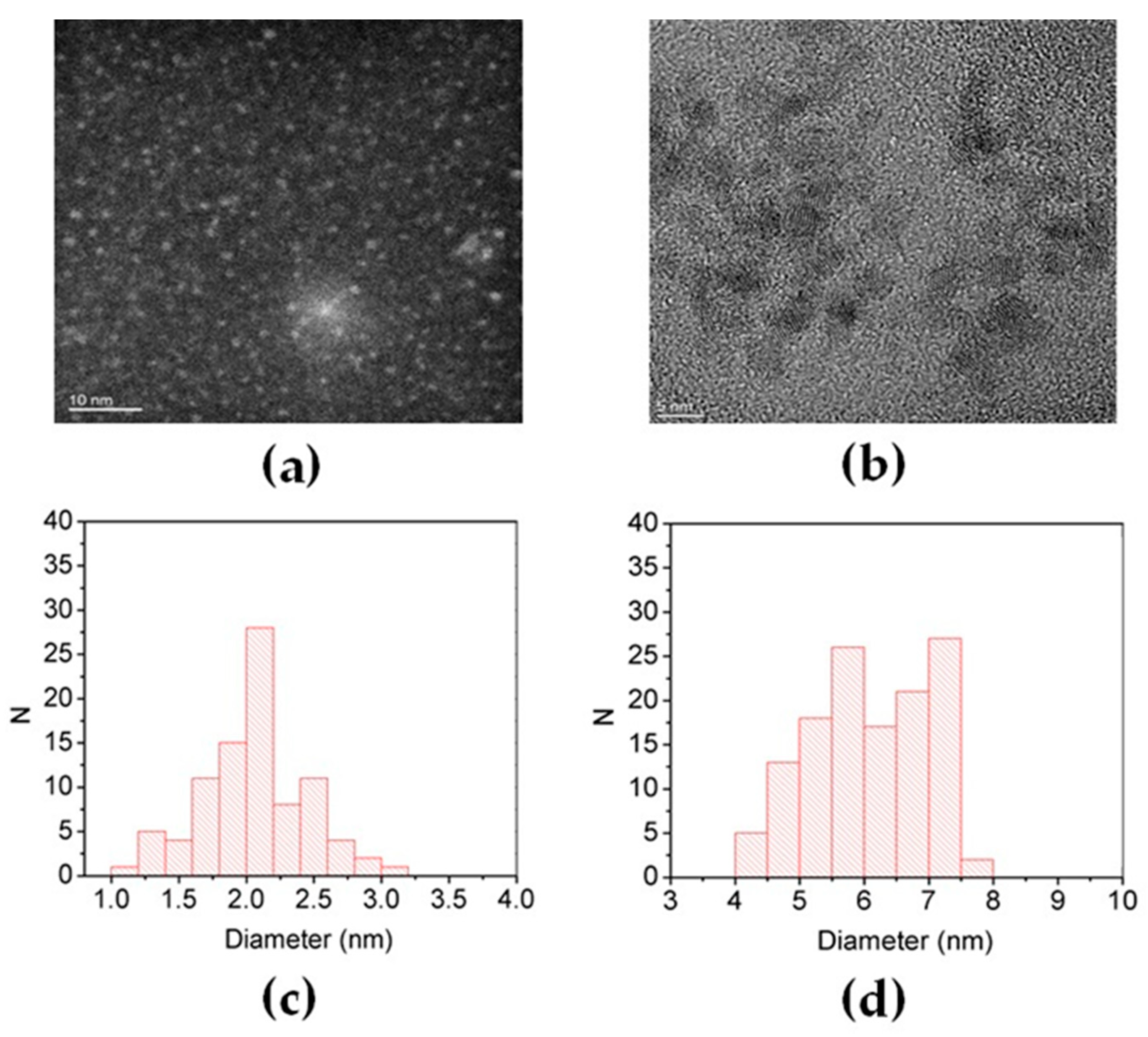
3.1.3. Structural and Morphological Characterization of CdTe QDs via In Situ Route

In Figure 5 reports the HAADF-STEM and phase contrast HRTEM for QDs produced in films annealed for 5 (green QDs) and 120 min (red QDs), respectively.
As depicted in Figure 5a,c, the HAADF-STEM acquired for the QDs produced in films annealed for 5 min shows crystalline particles with an average diameter estimated on 90 QDs with a confidence interval of 99% of d = 2.0 ± 0.4 nm.
Concerning the red QDs, the estimated average diameter is d = 6.0 ± 0.3 nm with a confidence interval of 99% estimated on 130 NPs (Figure 5b,d).
At a first glance, these results confirm once again that the developed method allows us to produce QDs with tunable size by modulating the annealing time directly within a polymeric matrix. However, the TEM and optical methods measurements show also some relatively small differences for the average size and size distribution determination. These differences can be attributed to both optical and structural measurements carried out in a thin film. Indeed, the optical methods are affected by the influence of the external shell that modulates the band gap [2,45] and therefore the size calculations, while the TEM measurement is affected by the observation of a limited amount of sample (not averaged on thousands of QDs as the optical spectroscopy), by the sample preparation (dissolution and dilution of the film and then its dropping over the TEM grid) and the technical difficulty to determine exactly the particle edge considering their small size and the presence of a not conductive matrix (polymer).

3.2. CdTe QDs via Ex Situ Route

To evaluate and compare the optical properties of the QDs grown directly in the polymer matrix (in situ), with that of the CdTe QDs grown in solution, the latter were incorporated into the polymer after their synthesis (ex situ).

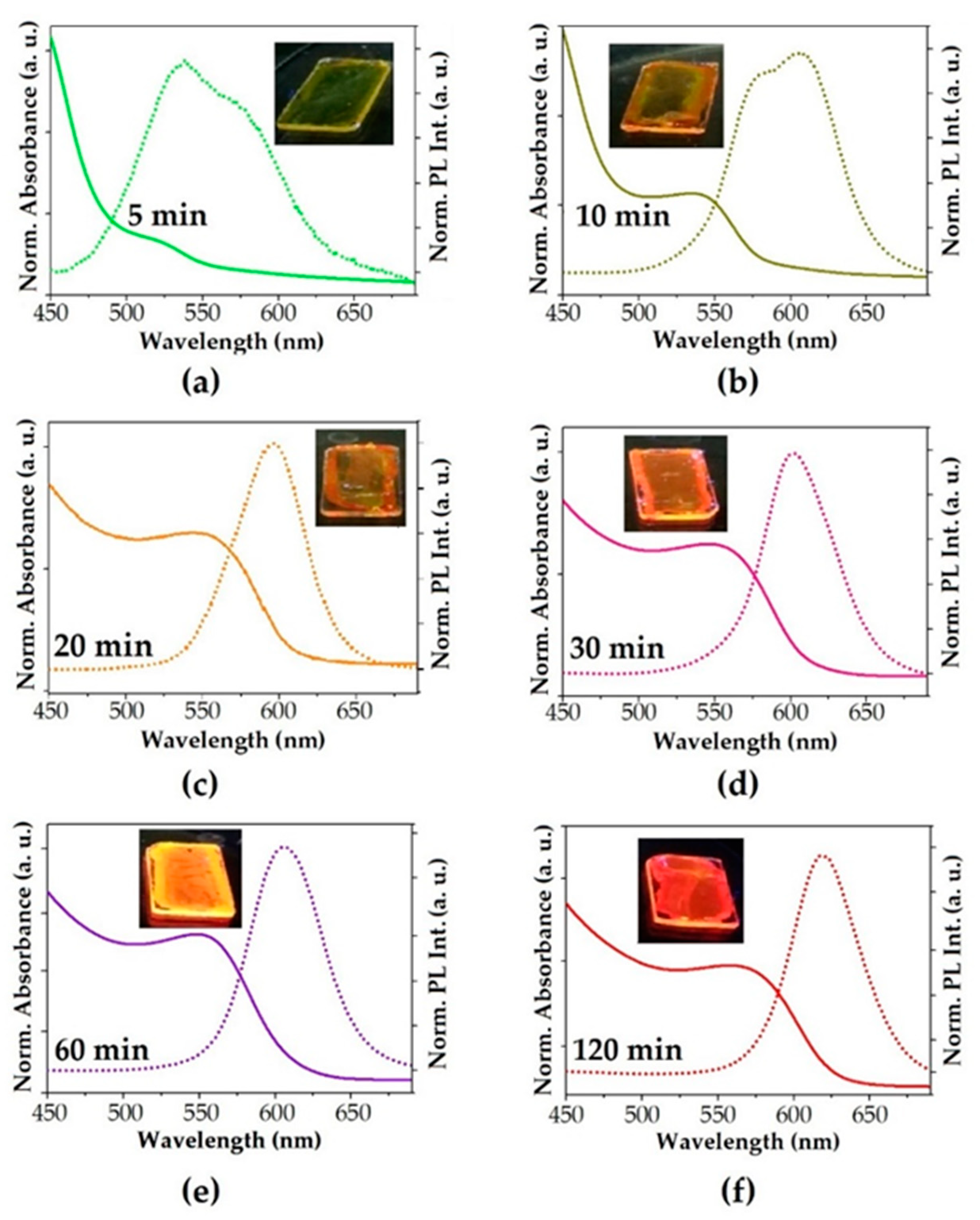
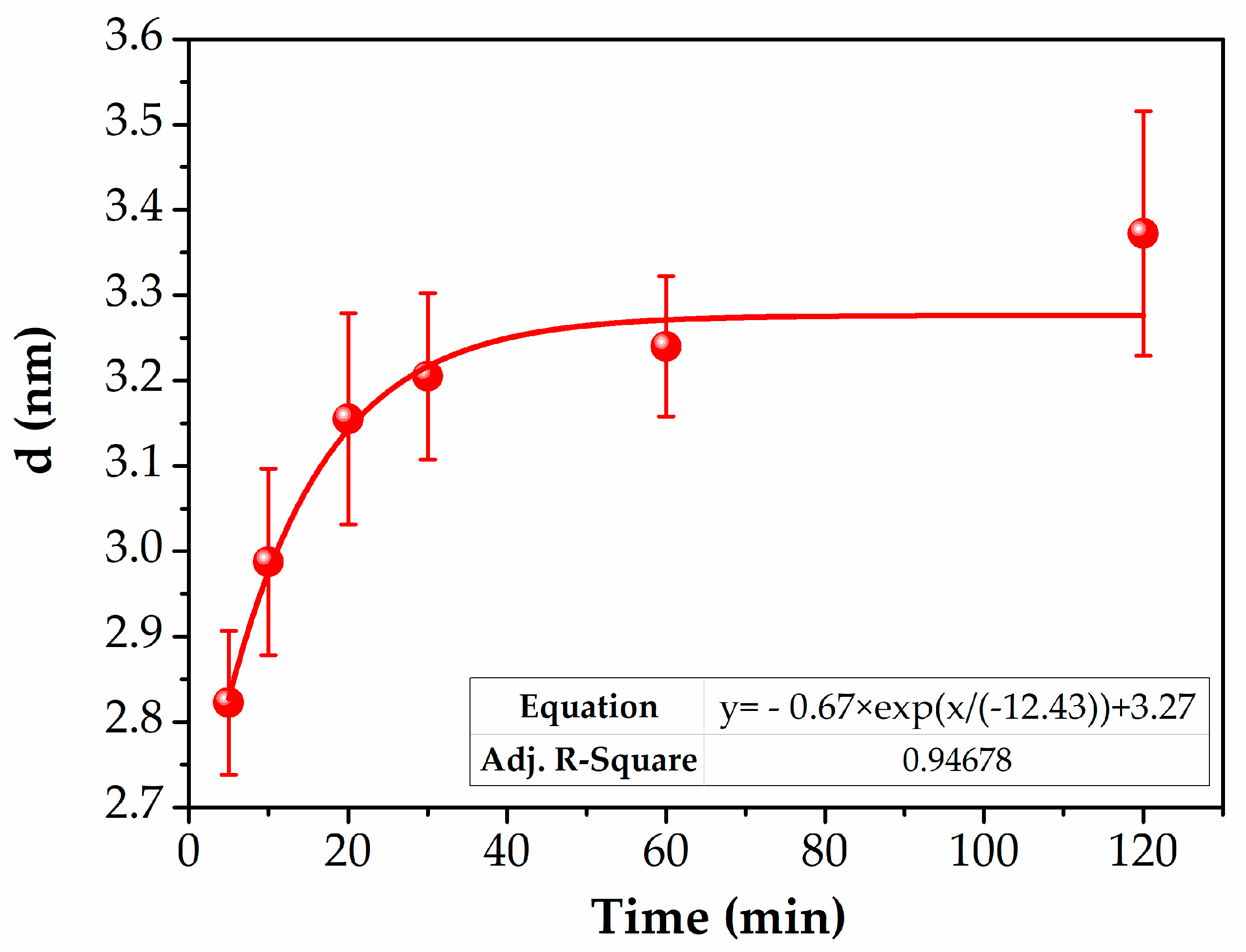
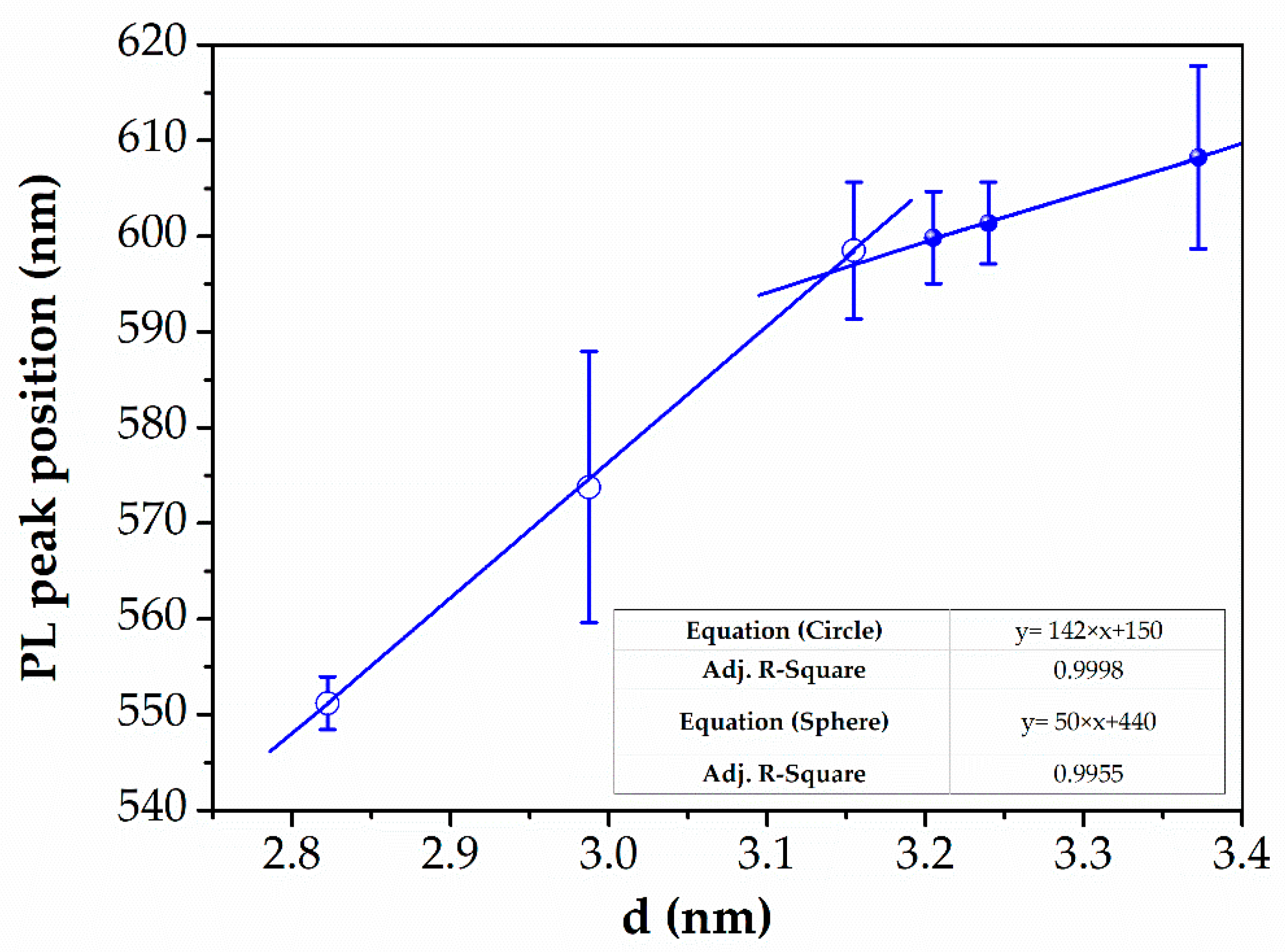
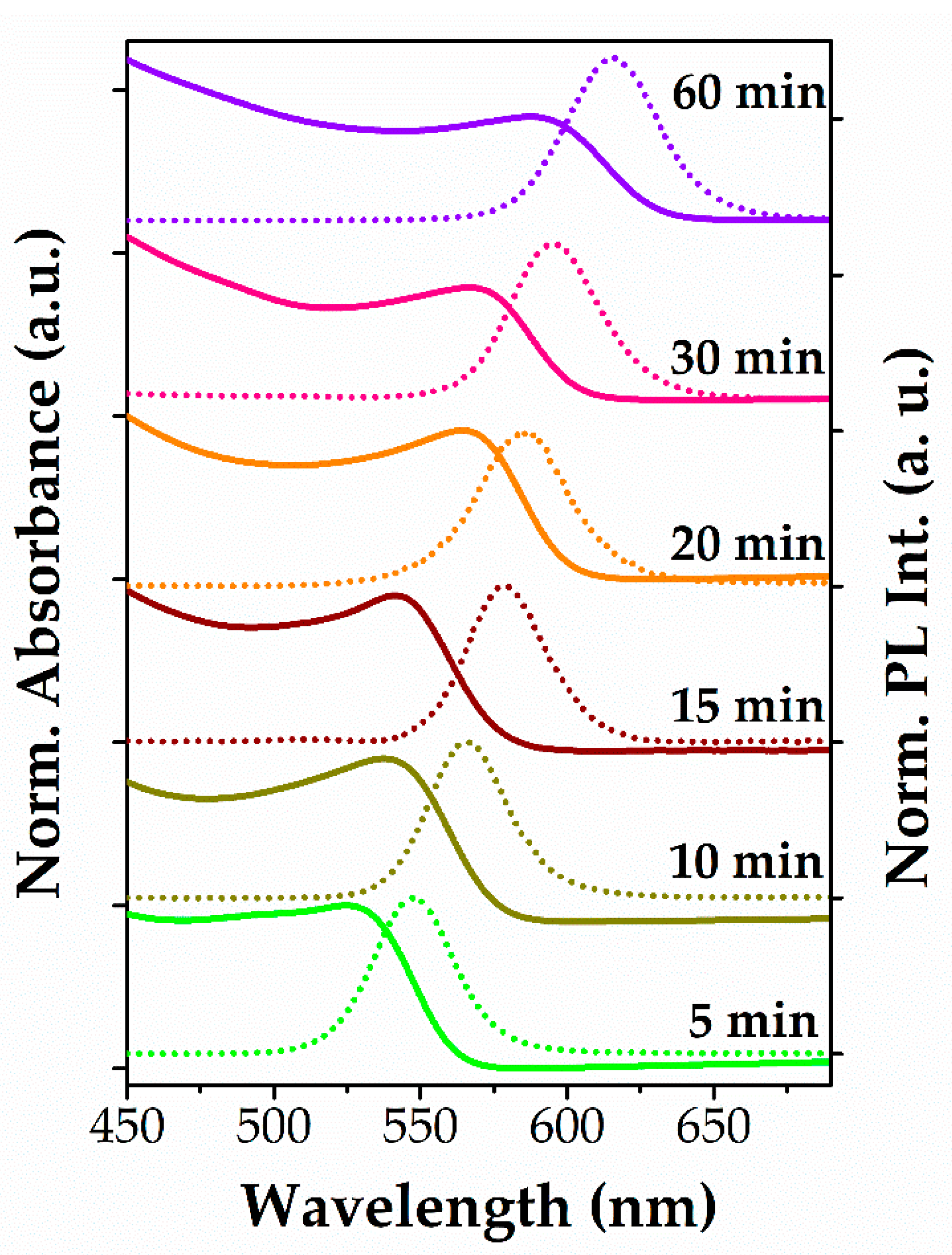
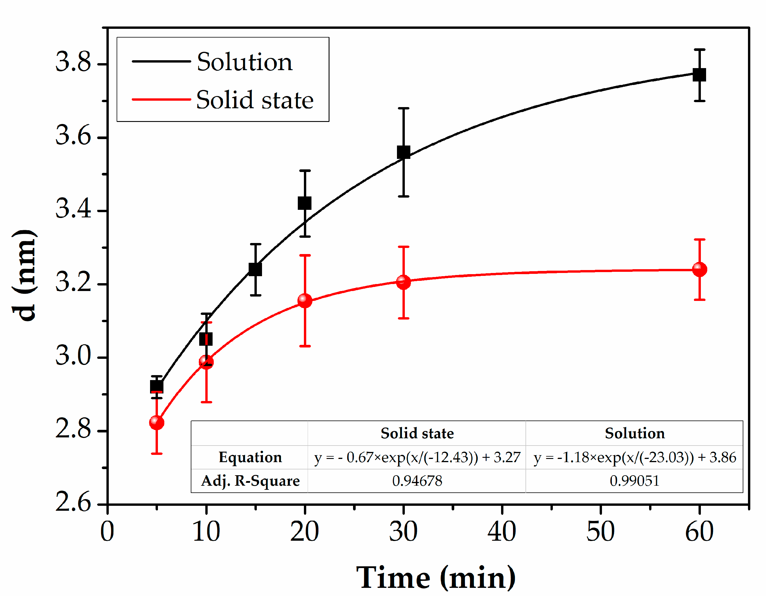
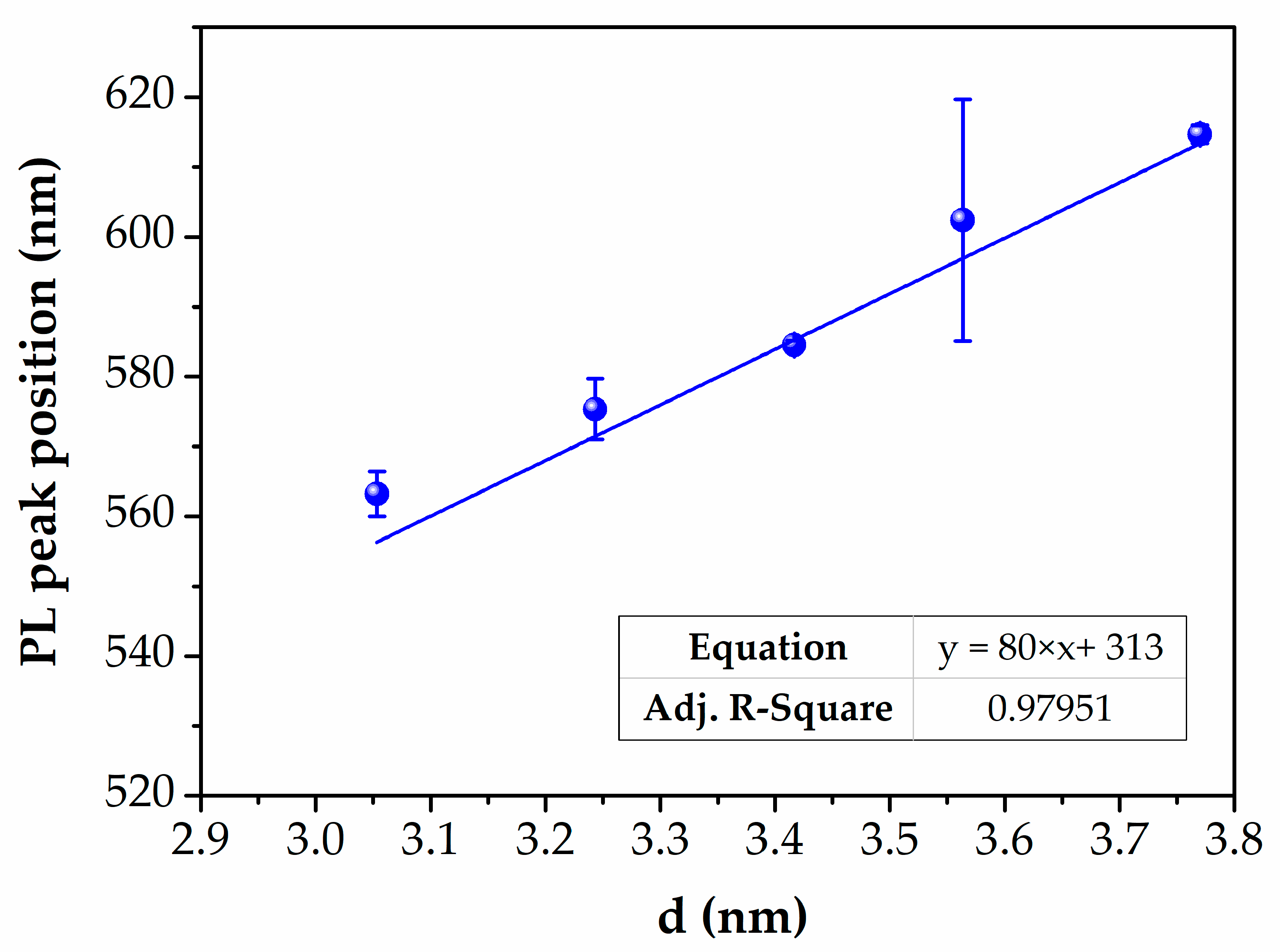
3.2.1. Optical Properties of CdTe QDs in Solution

Figure 6 reports the absorption and emission spectra of the CdTe QDs via an ex situ route,which are synthesized in different reaction times of 5, 10, 15, 20 30 and 60 min, showing that the absorption and emission encompass the entire visible range.
For each sample, the absorption spectra in Figure 6 show well distinct absorption maximum of the first electronic transition that allows the calculation of the particle size as reported in Table 3. The table also reportS the values of the PL maxima and their FWHM.
The comparison of the time course of the QDs grown both in solid state and in solution is reported in Figure 7. Here it is possible to observe that the curves trend is different and, in particular, the size of the QDs increases more rapidly in solution than in the film. Such a finding is convincingly pointed out by the sizes’ asymptotic value, which is 3.8 and 3.3 nm for CdTe QDs grown in solution and in solid state, respectively. This behavior confirms that a limited mobility of the atoms within the film prevents the growth of the QDs and their ripening process. This is further witnessed by the FWHM values of the PL peaks in film and solution (Table 2 and Table 3). Indeed, in the film, the FWHM values range from 54 to 80 nm, while in the case of solution, the PL bands are narrower (34–40 nm). This finding suggests that the formation of the CdTe nanocrystals in solution occurs by means of a simultaneous and homogeneous burst of nucleation, which is succeeded by a uniform growth of the nanoparticles (Ostwald ripening) [47,48].
Even in the case of the CdTe QDs grown in solution the PL peak position linearly shifts toward higher wavelengths as the calculated d value increases (Figure 8), indicating that the PL emission properties of the colloidal solutions depend only on the size of the CdTe nanocrystals.

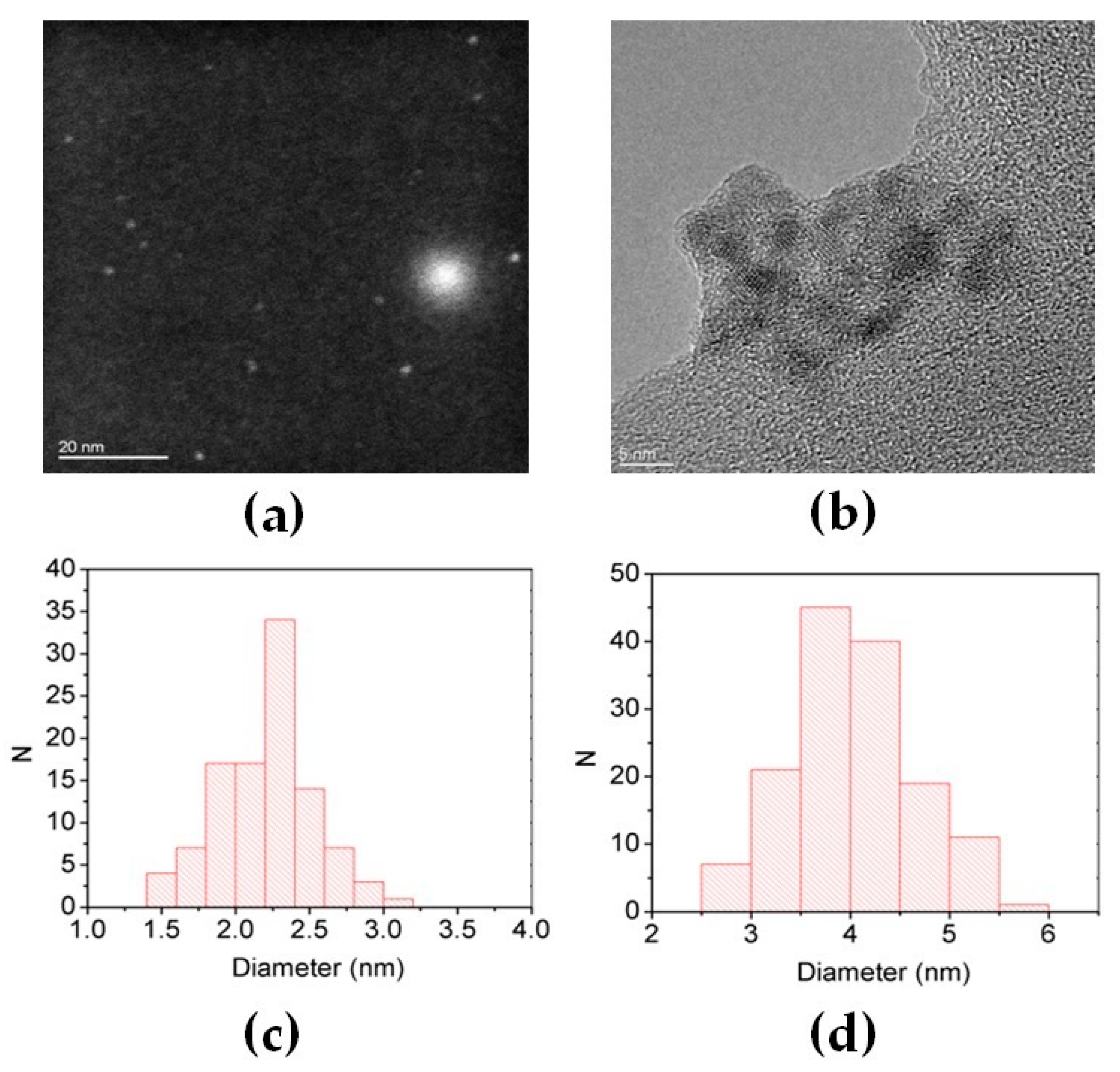
3.2.2. Structural and Morphological Characterization of CdTe QDs via Ex Situ Route

An in-depth analysis of the HAADF-STEM and TEM images allowed for a better estimation of the particles size grown in solution. The HAADF-STEM micrographs for CdTe QDs synthesized using a time reaction of 5 min shows an average diameter of 2.2 nm with a standard deviation of 0.45 nm, which is estimated on a number of 104 NPs (Figure 9a,c). Therefore, with a confidence interval of 99%, we assumed an average diameter value of d = 2.2 ± 0.2 nm.
As regards the red CdTe QDs synthesized using a reaction time of 30 min, the HRTEM images exhibit a diameter of 4 nm with a standard deviation of 0.65 nm estimated on a number of 144 QDs (Figure 9b,d). It is possible to assume an average diameter of d = 4.0 ± 0.2 nm.
The QDs particle size determined with TEM is in good agreement with the one calculated with the optical analysis, especially for larger particles.
In the case of TEM measurements of the particles grown in solution, the sizes and size distribution are clearly more in agreement than the ones obtained in thin film, because the effect of the polymer is avoided and the QDs preparation (synthesis in solution and TEM grid preparation) allows a uniform QDs observation even if few QDs are observed.

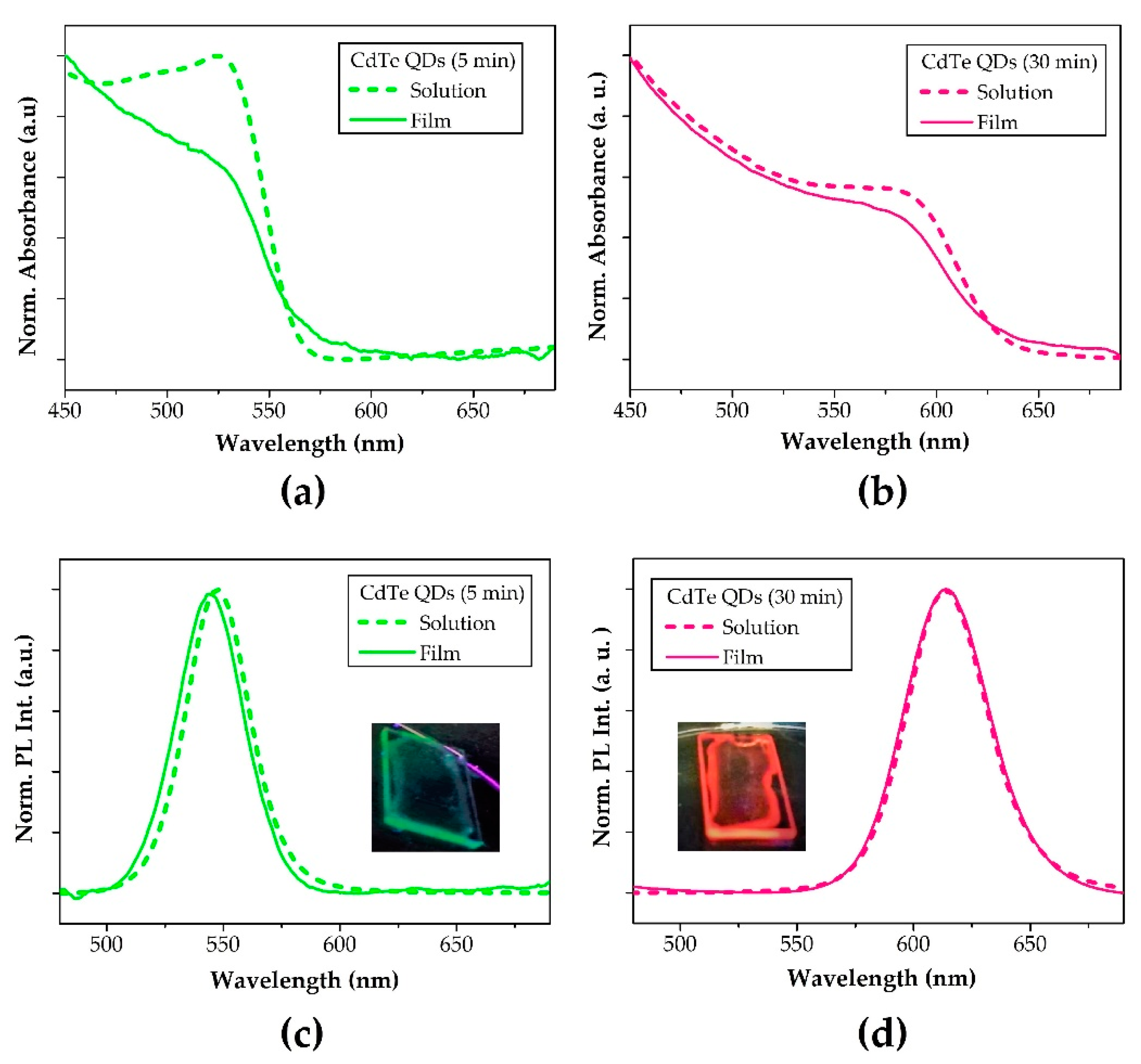
3.2.3. Optical Properties of CdTe QDs Encapsulated in Polymer Matrix via Ex Situ Route

To evaluate the effect of the polymer on the QDs prepared by ex situ routes, the absorption and PL properties of the films formed by the encapsulation of CdTe QDs in the polymer are investigated. In particular, the hybrid films are produced by loading the PMMA matrix with the CdTe QDs grown for 5 and 30 min, emitting green and orange/red light, respectively (Figure 10a–d).
It is important to highlight that the QDs prepared in solution are soluble after precipitation in organic solvents. This means that at the surface of the QDs, the isostearate molecules present are probably bound at the metal free binding site. Their solubility allows to mixing the CdTe QDs with PMMA.
The nanocomposites prepared by incorporating the green and red emitting CdTe QDs in the PMMA matrix did not produce significant changes in the absorption and the PL spectra of the nanocrystals after 5 and 30 min of the annealing process. The slight lowering in the definition of the absorption peak of the nanocomposite films (solid lines Figure 10a,b) with respect to that of the respective solutions (dashes lines Figure 10a,b) can be likely due to the interaction between the polymer and the CdTe nanoparticles. In particular, the broadening of the first electronic transition is probably due to the interaction of QDs and polymer. Indeed, when the QDs are close packed the localized (in one isolated QD) electronic transition is delocalized over a macroscopically large number of nanocrystals [49]. On the other hands, the PL spectra of the films (solid lines Figure 10c,d) fairly reproduce those of the solutions (dashed lines Figure 10c,d).
This means that the isostearate surrounding the QDs blocks all the surface defects and the PL properties in terms of PL shift of the CdTe QDs still remain constant after the encapsulation process. Given such considerations, the cadmium and tellurium precursors employed in this study are valid candidates to produce CdTe QDs suitable for display manufacturing applications.

4. Conclusions

The synthesis of the CdTe QDs was obtained via a cadmium isostearate Cd(ISA)2 precursor decomposition carried out at relatively low decomposition temperature. The reaction conditions both in polymer (PMMA) and is solution (ODE) requested the temperature of 150 °C to produce CdTe QDs with PL emission properties tunable in a range of about 70 nm (from green to red). This condition is particularly attractive for the possible application of the nanocomposite for electro-optical device manufacturing, because the polymer will be destroyed, and the device too can better withstand these conditions.
The time course analysis of the CdTe QDs formation showed the possibility obtaining CdTe QDs with an optical PL emission from green to red. The analysis of the FWHM of the QDs PL spectra, which is larger in the solid state than the one in solution, indicates that in the solid state the QDs growth is less homogeneous than in solution. This evidence is caused by the low mobility of the atoms in the solid state, which causes a non-uniform nuclei growth with more surface defects.
The perspective opened by this work to obtain QDs of different size maintaining constant the film chemical formulation over time is of great importance for the next application of direct laser patterning of the CdTe QDs. Indeed, a suitable local temperature increase can be reached by changing only the laser parameters allowing a selective QDs growth. In the meantime, further work is in progress to characterize and improve the photoluminescent quantum yield and the photostability of the in situ generated CdTe QDs.

Author Contributions

Conceptualization: F.A.; methodology: R.C. and F.L.; software: R.C. and F.L.; validation: F.L. and R.C.; formal analysis: F.L. and R.C.; investigation: F.L and R.C.; resources: F.A.; data curation, F.L., R.C. and F.A.; writing—original draft preparation: R.C., F.L. and F.A.; writing—review and editing: F.L., R.C. and F.A.; supervision: F.A.; project administration: F.A.; funding acquisition: F.A. All authors have read and agreed to the published version of the manuscript.

Funding

This research was funded by the European Union Horizon 2020 research and innovation programme (Photonics21, public private partnersghip), Grant Agreement n. 779373, project MILEDI (MIcro quantum dot Light Emitting diode and organic light emitting diodes DIrect patterning.

Institutional Review Board Statement

Not applicable.

Informed Consent Statement

Not applicable.

Data Availability Statement

Not applicable.

Acknowledgments

The authors thank Rosa Maria Montereali, Head of Photonics Micro and Nanostructures Laboratory, ENEA Frascati, for her helpful advice and suggestions. The authors thank Andrea Migliori, researcher at CNR-IMM (Bologna) for his technical support on TEM analysis. The authors thank Pietro Tagliatesta, professor at University of Rome Tor Vergata for his technical support on 1H-NMR analysis.

Conflicts of Interest

The authors declare no conflict of interest.

References

  1. Rogach, A. (Ed.) Semiconductor Nanocrystal Quantum Dots: Synthesis, Assembly, Spectroscopy and Applications; Springer: Wien, Austria, 2008; ISBN 978-3-211-75235-7. [Google Scholar]
  2. Jasieniak, J.; Califano, M.; Watkins, S.E. Size-Dependent Valence and Conduction Band-Edge Energies of Semiconductor Nanocrystals. ACS Nano 2011, 5, 5888–5902. [Google Scholar] [CrossRef] [PubMed]
  3. Christodoulou, S.; Vaccaro, G.; Pinchetti, V.; Donato, F.D.; Grim, J.Q.; Casu, A.; Genovese, A.; Vicidomini, G.; Diaspro, A.; Brovelli, S.; et al. Synthesis of Highly Luminescent Wurtzite CdSe/CdS Giant-Shell Nanocrystals Using a Fast Continuous Injection Route. J. Mater. Chem. C 2014, 2, 3439–3447. [Google Scholar] [CrossRef] [Green Version]
  4. Bae, W.K.; Char, K.; Hur, H.; Lee, S. Single-Step Synthesis of Quantum Dots with Chemical Composition Gradients. Chem. Mater. 2008, 20, 531–539. [Google Scholar] [CrossRef]
  5. Jang, E.; Jun, S.; Jang, H.; Lim, J.; Kim, B.; Kim, Y. White-Light-Emitting Diodes with Quantum Dot Color Converters for Display Backlights. Adv. Mater. 2010, 22, 3076–3080. [Google Scholar] [CrossRef]
  6. Hood, M.A.; Mari, M.; Muñoz-Espí, R. Synthetic Strategies in the Preparation of Polymer/Inorganic Hybrid Nanoparticles. Materials 2014, 7, 4057–4087. [Google Scholar] [CrossRef]
  7. Meinardi, F.; Colombo, A.; Velizhanin, K.A.; Simonutti, R.; Lorenzon, M.; Beverina, L.; Viswanatha, R.; Klimov, V.I.; Brovelli, S. Large-Area Luminescent Solar Concentrators Based on ‘Stokes-Shift-Engineered’ Nanocrystals in a Mass-Polymerized PMMA Matrix. Nat. Photonics 2014, 8, 392–399. [Google Scholar] [CrossRef]
  8. Gordillo, H.; Suárez, I.; Abargues, R.; Rodríguez-Cantó, P.; Albert, S.; Martínez-Pastor, J.P. Polymer/QDs Nanocomposites for Waveguiding Applications. Available online: https://www.hindawi.com/journals/jnm/2012/960201/ (accessed on 2 January 2021).
  9. Martynenko, I.V.; Litvin, A.P.; Purcell-Milton, F.; Baranov, A.V.; Fedorov, A.V.; Gun’ko, Y.K. Application of Semiconductor Quantum Dots in Bioimaging and Biosensing. J. Mater. Chem. B 2017, 5, 6701–6727. [Google Scholar] [CrossRef]
  10. Wang, P.; Zhang, Y.; Ruan, C.; Su, L.; Cui, H.; Yu, W.W. A Few Key Technologies of Quantum Dot Light-Emitting Diodes for Display. IEEE J. Sel. Top. Quantum Electron. 2017, 23, 1–12. [Google Scholar] [CrossRef]
  11. Qian, L.; Zheng, Y.; Xue, J.; Holloway, P.H. Stable and Efficient Quantum-Dot Light-Emitting Diodes Based on Solution-Processed Multilayer Structures. Nat. Photonics 2011, 5, 543–548. [Google Scholar] [CrossRef]
  12. Fischer, V.; Bannwarth, M.B.; Jakob, G.; Landfester, K.; Muñoz-Espí, R. Luminescent and Magnetoresponsive Multifunctional Chalcogenide/Polymer Hybrid Nanoparticles. J. Phys. Chem. C 2013, 117, 5999–6005. [Google Scholar] [CrossRef]
  13. Leventis, H.C.; King, S.P.; Sudlow, A.; Hill, M.S.; Molloy, K.C.; Haque, S.A. Nanostructured Hybrid Polymer−Inorganic Solar Cell Active Layers Formed by Controllable in Situ Growth of Semiconducting Sulfide Networks. Nano Lett. 2010, 10, 1253–1258. [Google Scholar] [CrossRef] [PubMed]
  14. Benedetto, F.D.; Camposeo, A.; Persano, L.; Laera, A.M.; Piscopiello, E.; Cingolani, R.; Tapfer, L.; Pisignano, D. Light-Emitting Nanocomposite CdS–Polymer Electrospun Fibres via in Situ Nanoparticle Generation. Nanoscale 2011, 3, 4234–4239. [Google Scholar] [CrossRef] [PubMed]
  15. Antolini, F.; Ghezelbash, A.; Esposito, C.; Trave, E.; Tapfer, L.; Korgel, B.A. Laser-Induced Nanocomposite Formation for Printed Nanoelectronics. Mater. Lett. 2006, 60, 1095–1098. [Google Scholar] [CrossRef]
  16. Camposeo, A.; Polo, M.; Neves, A.A.R.; Fragouli, D.; Persano, L.; Molle, S.; Laera, A.M.; Piscopiello, E.; Resta, V.; Athanassiou, A.; et al. Multi-Photon in Situ Synthesis and Patterning of Polymer-Embedded Nanocrystals. J. Mater. Chem. 2012, 22, 9787–9793. [Google Scholar] [CrossRef]
  17. Arnold, C.B.; Piqué, A. Laser Direct-Write Processing. Mrs Bull. 2007, 32, 9–15. [Google Scholar] [CrossRef] [Green Version]
  18. Piqué, A.; Auyeung, R.C.Y.; Kim, H.; Charipar, N.A.; Mathews, S.A. Laser 3D Micro-Manufacturing. J. Phys. D Appl. Phys. 2016, 49, 223001. [Google Scholar] [CrossRef]
  19. Antolini, F.; Orazi, L. Quantum Dots Synthesis through Direct Laser Patterning: A Review. Front. Chem. 2019, 7. [Google Scholar] [CrossRef] [PubMed]
  20. Resta, V.; Laera, A.M.; Camposeo, A.; Piscopiello, E.; Persano, L.; Pisignano, D.; Tapfer, L. Spatially Confined CdS NCs in Situ Synthesis through Laser Irradiation of Suitable Unimolecular Precursor-Doped Polymer. J. Phys. Chem. C 2012, 116, 25119–25125. [Google Scholar] [CrossRef]
  21. Bansal, A.K.; Sajjad, M.T.; Antolini, F.; Stroea, L.; Gečys, P.; Raciukaitis, G.; André, P.; Hirzer, A.; Schmidt, V.; Ortolani, L.; et al. In Situ Formation and Photo Patterning of Emissive Quantum Dots in Small Organic Molecules. Nanoscale 2015, 7, 11163–11172. [Google Scholar] [CrossRef] [Green Version]
  22. Limosani, F.; Carcione, R.; Antolini, F. Formation of CdSe Quantum Dots from Single Source Precursor Obtained by Thermal and Laser Treatment. J. Vac. Sci. Technol. B 2019, 38, 012802. [Google Scholar] [CrossRef]
  23. Dorfs, D.; Franzl, T.; Osovsky, R.; Brumer, M.; Lifshitz, E.; Klar, T.A.; Eychmüller, A. Type-I and Type-II Nanoscale Heterostructures Based on CdTe Nanocrystals: A Comparative Study. Small 2008, 4, 1148–1152. [Google Scholar] [CrossRef] [PubMed]
  24. Haram, S.K.; Kshirsagar, A.; Gujarathi, Y.D.; Ingole, P.P.; Nene, O.A.; Markad, G.B.; Nanavati, S.P. Quantum Confinement in CdTe Quantum Dots: Investigation through Cyclic Voltammetry Supported by Density Functional Theory (DFT). J. Phys. Chem. C 2011, 115, 6243–6249. [Google Scholar] [CrossRef]
  25. Malik, M.A.; Afzaal, M.; O’Brien, P. Precursor Chemistry for Main Group Elements in Semiconducting Materials. Chem. Rev. 2010, 110, 4417–4446. [Google Scholar] [CrossRef] [PubMed]
  26. Resta, V.; Laera, A.M.; Piscopiello, E.; Schioppa, M.; Tapfer, L. Highly Efficient Precursors for Direct Synthesis of Tailored CdS Nanocrystals in Organic Polymers. J. Phys. Chem. C 2010, 114, 17311–17317. [Google Scholar] [CrossRef]
  27. Bansal, A.K.; Antolini, F.; Zhang, S.; Stroea, L.; Ortolani, L.; Lanzi, M.; Serra, E.; Allard, S.; Scherf, U.; Samuel, I.D.W. Highly Luminescent Colloidal CdS Quantum Dots with Efficient Near-Infrared Electroluminescence in Light-Emitting Diodes. J. Phys. Chem. C 2016, 120, 1871–1880. [Google Scholar] [CrossRef] [Green Version]
  28. Pradhan, N.; Katz, B.; Efrima, S. Synthesis of High-Quality Metal Sulfide Nanoparticles from Alkyl Xanthate Single Precursors in Alkylamine Solvents. J. Phys. Chem. B 2003, 107, 13843–13854. [Google Scholar] [CrossRef]
  29. Kedarnath, G.; Dey, S.; Jain, V.K.; Dey, G.K.; Varghese, B. 2-(N,N-Dimethylamino)Ethylselenolates of Cadmium(II): Syntheses, Structure of [Cd3(OAc)2(SeCH2CH2NMe2)4] and Their Use as Single Source Precursors for the Preparation of CdSe Nanoparticles. Polyhedron 2006, 25, 2383–2391. [Google Scholar] [CrossRef]
  30. Stroea, L.; Bansal, A.K.; Samuel, I.D.W.; Kowalski, S.; Allard, S.; Scherf, U.; Ortolani, L.; Cavallini, S.; Toffanin, S.; Antolini, F. Growth of Photoluminescent Cadmium Sulphide Quantum Dots from Soluble Single Source Precursors in Solution and in Film. Sci. Adv. Mater. 2015, 7, 1–14. [Google Scholar] [CrossRef]
  31. Chivers, T.; Ritch, J.S.; Robertson, S.D.; Konu, J.; Tuononen, H.M. New Insights into the Chemistry of Imidodiphosphinates from Investigations of Tellurium-Centered Systems. Acc. Chem. Res. 2010, 43, 1053–1062. [Google Scholar] [CrossRef] [PubMed]
  32. Yu, K.; Liu, X.; Zeng, Q.; Yang, M.; Ouyang, J.; Wang, X.; Tao, Y. The Formation Mechanism of Binary Semiconductor Nanomaterials: Shared by Single-Source and Dual-Source Precursor Approaches. Angew. Chem. Int. Ed. 2013, 52, 11034–11039. [Google Scholar] [CrossRef]
  33. Taukeer Khan, M.; Kaur, A.; Dhawan, S.K.; Chand, S. In-Situ Growth of Cadmium Telluride Nanocrystals in Poly(3-Hexylthiophene) Matrix for Photovoltaic Application. J. Appl. Phys. 2011, 110, 044509. [Google Scholar] [CrossRef]
  34. Antolini, F.; Ortolani, L. CdTe Quantum Dots Nanocomposite Films Obtained by Thermal Decomposition of Precursors Embedded in Polymeric Matrix. In Physics, Chemistry and Application of Nanostructures; World Scientific: Singapore, 2017; pp. 349–352. ISBN 978-981-322-452-0. [Google Scholar]
  35. Huang, Y.; Liu, J.; Yu, Y.; Zuo, S. Preparation and Multicolored Fluorescent Properties of CdTe Quantum Dots/Polymethylmethacrylate Composite Films. J. Alloy. Compd. 2015, 647, 578–584. [Google Scholar] [CrossRef]
  36. Kirkwood, N.; Monchen, J.O.V.; Crisp, R.W.; Grimaldi, G.; Bergstein, H.A.C.; du Fossé, I.; van der Stam, W.; Infante, I.; Houtepen, A.J. Finding and Fixing Traps in II–VI and III–V Colloidal Quantum Dots: The Importance of Z-Type Ligand Passivation. J. Am. Chem. Soc. 2018, 140, 15712–15723. [Google Scholar] [CrossRef] [Green Version]
  37. Kamal, J.S.; Omari, A.; Van Hoecke, K.; Zhao, Q.; Vantomme, A.; Vanhaecke, F.; Capek, R.K.; Hens, Z. Size-Dependent Optical Properties of Zinc Blende Cadmium Telluride Quantum Dots. J. Phys. Chem. C 2012, 116, 5049–5054. [Google Scholar] [CrossRef]
  38. García-Rodríguez, R.; Hendricks, M.P.; Cossairt, B.M.; Liu, H.; Owen, J.S. Conversion Reactions of Cadmium Chalcogenide Nanocrystal Precursors. Chem. Mater. 2013, 25, 1233–1249. [Google Scholar] [CrossRef]
  39. Algieri, L.; Rosato, R.; Mosca, M.E.; Protopapa, M.L.; Scalone, A.G.; Benedetto, F.D.; Bucci, L.; Tapfer, L. Green Light-Emitting CdTe Nanocrystals: Synthesis and Optical Characterizations. Phys. Status Solidi C 2015, 12, 147–152. [Google Scholar] [CrossRef]
  40. García-Rodríguez, R.; Liu, H. Mechanistic Study of the Synthesis of CdSe Nanocrystals: Release of Selenium. J. Am. Chem. Soc. 2012, 134, 1400–1403. [Google Scholar] [CrossRef]
  41. Liu, H.; Owen, J.S.; Alivisatos, A.P. Mechanistic Study of Precursor Evolution in Colloidal Group II−VI Semiconductor Nanocrystal Synthesis. J. Am. Chem. Soc. 2007, 129, 305–312. [Google Scholar] [CrossRef]
  42. LaMer, V.K.; Dinegar, R.H. Theory, Production and Mechanism of Formation of Monodispersed Hydrosols. J. Am. Chem. Soc. 1950, 72, 4847–4854. [Google Scholar] [CrossRef]
  43. Mutavdžić, D.; Xu, J.; Thakur, G.; Triulzi, R.; Kasas, S.; Jeremić, M.; Leblanc, R.; Radotić, K. Determination of the Size of Quantum Dots by Fluorescence Spectroscopy. Analyst 2011, 136, 2391–2396. [Google Scholar] [CrossRef] [PubMed]
  44. Huang, X.; Jing, L.; Kershaw, S.V.; Wei, X.; Ning, H.; Sun, X.; Rogach, A.L.; Gao, M. Narrowing the Photoluminescence of Aqueous CdTe Quantum Dots via Ostwald Ripening Suppression Realized by Programmed Dropwise Precursor Addition. J. Phys. Chem. C 2018, 122, 11109–11118. [Google Scholar] [CrossRef]
  45. Smith, A.M.; Nie, S. Semiconductor Nanocrystals: Structure, Properties, and Band Gap Engineering. Acc. Chem. Res. 2010, 43, 190–200. [Google Scholar] [CrossRef] [PubMed] [Green Version]
  46. Anderson, N.C.; Hendricks, M.P.; Choi, J.J.; Owen, J.S. Ligand Exchange and the Stoichiometry of Metal Chalcogenide Nanocrystals: Spectroscopic Observation of Facile Metal-Carboxylate Displacement and Binding. J. Am. Chem. Soc. 2013, 135, 18536–18548. [Google Scholar] [CrossRef] [PubMed] [Green Version]
  47. Peng, X.; Wickham, J.; Alivisatos, A.P. Kinetics of II-VI and III-V Colloidal Semiconductor Nanocrystal Growth:  “Focusing” of Size Distributions. J. Am. Chem. Soc. 1998, 120, 5343–5344. [Google Scholar] [CrossRef]
  48. Vreeland, E.C.; Watt, J.; Schober, G.B.; Hance, B.G.; Austin, M.J.; Price, A.D.; Fellows, B.D.; Monson, T.C.; Hudak, N.S.; Maldonado-Camargo, L.; et al. Enhanced Nanoparticle Size Control by Extending LaMer’s Mechanism. Chem. Mater. 2015, 27, 6059–6066. [Google Scholar] [CrossRef]
  49. Cao, X.; Li, C.M.; Bao, H.; Bao, Q.; Dong, H. Fabrication of Strongly Fluorescent Quantum Dot−Polymer Composite in Aqueous Solution. Chem. Mater. 2007, 19, 3773–3779. [Google Scholar] [CrossRef]
Scheme 1. Scheme of the synthesis of the cadmium isostearate, trioctylphosphine telluride and the CdTe quantum dots (QDs).
Crystals 11 00253 sch001
Figure 1. Normalized emission spectra of CdTe QDs synthetized in film at different temperatures: 120 °C (black line), 150 °C (blue line) and 180 °C (purple line): (a) at 5 min and (b) 20 min.
Crystals 11 00253 g001
Figure 2. Absorption and normalized PL spectra of films annealed at 150 °C for (a) 5, (b) 10, (c) 20, (d) 30, (e) 60, and (f) 120 min under vacuum. Inset: photographs of the films acquired under UV lamp at 365 nm.
Crystals 11 00253 g002
Figure 3. Estimated average size of the CdTe nanocrystals (d) as a function of the annealing time.
Crystals 11 00253 g003
Figure 4. PL peak position as a function of CdTe QDs size grown in film (the first linear fit for the growth of CdTe QDs from 5 to 20 min is reported as solid line and circles; the second linear fit for the growth of CdTe QDs from 30 to 120 min is reported as solid line and spheres).
Crystals 11 00253 g004
Figure 5. Images taken by (a) High Angle Annular Dark Field (HAADF)-STEM and (b) phase contrast HRTEM for green and red QDs produced in films annealed for 5 and 120 min at 150 °C, respectively. Distribution of the number of particles (N) as a function of the diameter of the particles for (c) green and (d) red QDs.
Crystals 11 00253 g005
Figure 6. Normalized absorption and PL emission spectra for CdTe QDs via ex situ route, synthesized at different reaction times.
Crystals 11 00253 g006
Figure 7. Calculated size of CdTe QDs versus time course both in solid state (red line same curve of Figure 3) and in solution (black line).
Crystals 11 00253 g007
Figure 8. PL peak position as a function of CdTe QDs size grown in solution (the linear fit is reported as a solid line).
Crystals 11 00253 g008
Figure 9. Images obtained by (a) HAADF-STEM and (b) phase contrast HRTEM for green and red QDs produced using as time of reaction of 4 and 30 min, respectively. Distribution of the number of particles (N) as a function of the diameter of the particles for (c) green and (d) red QDs.
Crystals 11 00253 g009
Figure 10. Normalized absorption spectra of the CdTe QDs prepared at 150 °C after 5 (a) and 30 (b) minutes of annealing in solution (dashed line) and after encapsulation in the polymer (solid line). Normalized PL spectra of the CdTe QDs prepared after 5 (c) and 30 (d) minutes of annealing in solution (dashed line) and after encapsulation in the polymer (solid line). Inset: photographs of the films acquired under the UV lamp at 365 nm.
Crystals 11 00253 g010
Table 1. Photoluminescent (PL) peak position as a function of annealing time and temperature.
Annealing
Temperature (°C)
PL Max (nm)
5 min
PL Max (nm)
20 min
∆PL (nm)
120-587-
15052660175
18059761821
Table 2. Calculated QDs size (d) and PL bands parameters as a function of the annealing time.
Growth Time (min)D (nm)Averaged PL Peak Position (nm)PL FWHM
(nm)
52.82 ± 0.08551 * ± 380 ± 14
102.99 ± 0.11573 * ± 1460 ± 10
203.16 ± 0.12598 ± 757 ± 3
303.21 ± 0.10600 ± 556 ± 1
603.24 ± 0.08601 ± 455 ± 1
1203.37 ± 0.14608 ± 1054 ± 1
* The averaged PL peak position is calculated approximating the double emission peak as a single Gaussian function.
Table 3. Deconvolution derived parameters of size (d), PL peak position and full width at half maximum (PL FWHM).
Growth Time (min)D (nm)Averaged PL Peak
Position (nm)
PL FWHM (nm)
52.92 ± 0.03539 ± 835 ± 4
103.05 ± 0.07563 ± 334 ± 1
153.24 ± 0.07575 ± 435 ± 2
203.42 ± 0.09584 ± 136 ± 5
303.56 ± 0.12602 ± 1738 ± 3
603.77 ± 0.07614 ± 140 ± 3
Publisher’s Note: MDPI stays neutral with regard to jurisdictional claims in published maps and institutional affiliations.

