Article

Evaluation of the Performance of Published Point Defect Parameter Sets in Cone and Body Phase of a 300 mm Czochralski Silicon Crystal

1
Institute of Numerical Modelling, University of Latvia, Jelgavas Street 3, LV-1004 Riga, Latvia
2
Siltronic AG, Einsteinstraße 172-Tower B/Blue Tower, 81677 München, Germany
*
Author to whom correspondence should be addressed.
Submission received: 26 March 2021 / Revised: 16 April 2021 / Accepted: 19 April 2021 / Published: 21 April 2021
(This article belongs to the Special Issue Modeling of Crystal Growth)

Abstract

:
Prediction and adjustment of point defect (vacancies and self-interstitials) distribution in silicon crystals is of utmost importance for microelectronic applications. The simulation of growth processes is widely applied for process development and quite a few different sets of point defect parameters have been proposed. In this paper the transient temperature, thermal stress and point defect distributions are simulated for 300 mm Czochralski growth of the whole crystal including cone and cylindrical growth phases. Simulations with 12 different published point defect parameter sets are compared to the experimentally measured interstitial–vacancy boundary. The results are evaluated for standard and adjusted parameter sets and generally the best agreement in the whole crystal is found for models considering the effect of thermal stress on the equilibrium point defect concentration.

1. Introduction

The Czochralski (Cz) process is the method of choice for the production of silicon (Si) crystals for microelectronics applications. As the feature size of electronic devices is steadily decreasing, reduction of the size and number of grown-in defects as voids and self-interstitial agglomerates in Si wafers is of utmost importance for the process development. Accordingly, the distribution of intrinsic point defects (PD: vacancies, V, and self-interstitials, I)—the source of possible larger defect agglomerates—must be predicted and controlled very precisely during the crystal growth process.
The PD concentration depends on the thermal gradient and pulling velocity. The prevalent point defect type can be simply predicted by the v / G criterion as shown by Voronkov [1], where v is the crystal growth rate (equal to the pull rate V under steady-state conditions) and G is the temperature gradient in the crystal at the crystallization interface. The 2D axisymmetric numerical simulation of vacancy and interstitial concentrations considering incorporation, diffusion, convection and recombination validates the concept for different process parameters [2,3] and opens the way for process optimization regarding the defect distribution and reduction [4,5].
The global thermal modeling of the Cz process was started in the 1990s [6,7,8]. Quasi-steady and transient 2D models considered radiation heat transfer between heater, insulation, crucible and Si melt and crystal, as well as conduction in solid bodies and melt, allowing for the optimization of hot-zone and pulling velocity. Later simulation of the point defect distribution in the crystal domain was added [2,3,4,9,10]. Transient modeling of both the heat transfer and PD distribution is necessary since the Cz process is transient in reality, and the start and end cones are a considerable part of the whole growth process.
In the next step of PD model development [11], the effect of thermal stress on the point defect distribution was included. While the stress effect was first theoretically examined for a 150 mm crystal [12,13] and found out to be weak, later experimental evidence for a larger crystal with a diameter of 300 mm [14] demonstrated its importance for industrial-size crystals. This topic received greater attention only in the 2010s by the works of Vanhellemont [15,16,17]. Stress changes PD formation enthalpy, affecting the equilibrium concentration and the critical value of v / G , which has been confirmed experimentally [18] and explained theoretically [19]. Since the stress generally increases with the crystal size, this effect is more important for large crystals and is actively investigated nowadays [20,21,22,23].
While the PD parameter sets proposed by different groups are validated and fine-tuned to improve agreement with experiments in the body phase [3,4,20,23,24,25,26] (we are not aware of works comparing simulation results with experiment in the cone), they vary considerably. One of the possible reasons for such discrepancies is uncertainties in the global heat transfer (e.g., due to imprecise material properties) since the point defect distribution is sensitive to the temperature field in the crystal. Thus, two PD parameter sets cannot be simply compared if they were derived based on different heat transfer models. A detailed comparison of the performance of published PD parameter sets for the same experiment is not available in the literature.
In the present work, the software CZ-Trans is used for dynamic simulations of the temperature field, phase boundaries [27] and PD distribution in the crystal [28]. The novelty is that we (i) apply an improved and numerically more precise CZ-Trans model; (ii) simulate 12 different PD parameter sets using the same thermal conditions; (iii) compare simulation results with the experimental PD distribution in the whole crystal, including start and end cones; (iv) adjust PD parameters for 1 position in the crystal and find the parameter sets with the best agreement to experiment.

2. Growth Experiment

A 300 mm (12 inch) Cz silicon single crystal growth experiment carried out at Siltronic AG was selected, see Figure 1. The pull rate was slowly changed during the growth, which resulted in different radial positions of the I-V boundary (IVB) along the crystal length. The minority carrier lifetime in the cone, body (cylinder) and endcone was measured by the microwave photoconductivity decay (µ-PCD) method, which revealed the IVB position [3,29], while the lateral photovoltage scanning (LPS) measurements (not shown) were used to investigate the crystallization interface shape.
The cone of the grown crystal was completely interstitial-rich but starting from the shouldering stage (transition from cone to cylindrical growth), defined as the crystal length L = 0 , a vacancy-rich region developed near the crystal axis and was present throughout the whole body phase. A more complicated structure developed near the endcone and the vacancy region in the center reached the crystal surface around L = 1200 mm.
What is also important is the crystallization interface shape, which was extracted from the LPS measurements or, for crystal parts where they were unavailable, from µ-PCD data. The measured crystallization interface deflection H C as a function of crystal length is plotted in Figure 2, while the interface shapes are depicted in Figure 3. Since the melt flow was not directly modeled, this information was used to improve the agreement between simulations and experiment as the interface shape affects both the thermal stress and point defect distribution.

3. Numerical Model

3.1. Heat Transfer and Phase Boundaries

The program CZ-Trans  [27] was used to model the transient heat transfer in the Cz system and the changing phase boundaries. The model was axisymmetric, and the temperature field T ( r , z ) was calculated in the crystal, melt, crucible and heat shield domains while a simple integral model was used for the heater to calculate its time-dependent temperature as a function of the heater power change. Radiative heat transfer between surfaces was considered. Since the crystal was pulled upwards, both the convection and diffusion terms were included in the temperature equation
T t + V · T = · ( λ c T ) ,
where λ c is the thermal conductivity and V is the crystal pull rate, which has only a vertical component V z = V .
While the melt flow was not simulated, to correctly capture the crystallization interface shapes its influence was approximated by (i) homogeneous but time-dependent melt thermal conductivity λ m ( t ) and (ii) redistribution of the heat flux densities along the crystallization interface [30]. For the crystal λ c ( T ) = 98.89 9.43 × 10 2 T + 2.89 × 10 5 T 2 (in W / m / K ) was used; emissivities were 0.64 and 0.30 for the solid and liquid Si, respectively. The melting point of silicon T 0 = 1685 K .
For a more precise numerical modeling of the heat transfer (especially at the crystallization interface, since it affects the crystal growth rate), the possibility of using high-order finite elements was implemented in CZ-Trans. The developed temperature solver uses the open-source finite element library deal.II [31]. While the solver supports arbitrary element orders, from a practical point of view a good balance between the accuracy and performance is achieved for second-order elements (9-node quadrilaterals).
Since a quad-only mesh is required for deal.II, it was introduced for the crystal, melt and crucible domains. Where possible, a structured grid was generated by CZ-Trans, otherwise an unstructured mesh was created using Gmsh [32].
Newton’s method with a step length of 1 was employed to deal with the non-linearities, such as the temperature-dependent thermal conductivity. The obtained temperature field on second-order finite elements in the crystal was used to calculate the thermal stress and point defect distribution on the same mesh.

3.2. Point Defects

3.2.1. Governing Equations

The conservation equations for point defects can be written in a general form as
C t + V · C = · J + k r C I eq C V eq C I C V ,
with: C = C I , C V —point defect concentrations, C eq —equilibrium point defect concentration, D—diffusion coefficient, k r —reaction constant for recombination. The zero isoline of Δ = C I C V is the I-V boundary (IVB) [1]. For convenience, we introduce two non-negative variables Δ I = max ( Δ , 0 ) and Δ V = max ( Δ , 0 ) for interstitial-rich and vacancy-rich regions, respectively.
The diffusive flux of the point defects, J , is given by
J = D C + Q D k T 2 C T ,
where Q is the activation enthalpy for thermal diffusion and k = 8.617   ×   10 5 e V / K is the Boltzmann constant. Q > 0 means an uphill PD drift—in the direction of T, from a colder to a hotter crystal part since the drift velocity is given by v drift = D ( Q / ( k T ) ) = D Q / ( k T 2 ) T  [33]. Note that Q < 0 is also a valid value. The definition of the thermal diffusion term (its sign) is not consistent in the literature, therefore some PD parameter sets [18,34,35,36] were converted to match the formulation used in this study.
The temperature dependences of the point defect properties are given by
D = D 0 exp ( H m k T ) ,
C eq = C 0 exp ( H f + Δ H f k T ) ,
k r = 4 π a r D I + D V exp ( Δ G r k T ) ,
where D 0 and C 0 are prefactors; H m is the migration energy, H f and Δ H f are formation enthalpy and its change due to the thermal stress, respectively; a r is the capture radius and Δ G r is the energy barrier for recombination. The formation entropy is included in C 0 .
The critical value of the Voronkov parameter ξ = v / G corresponding to the present formulation, Equations (2) and (3), is [18,33,37]:
ξ crit = C I eq D I ( H av f Q I ) C V eq D V ( H av f Q V ) C V C I k T 0 2 , H av f = H I f + H V f 2 ,
where all quantities are evaluated at the melting point (MP) of Si, C V = C V eq and C I = C I eq . The crystal is interstitial-rich for ξ < ξ crit and vacancy-rich for ξ > ξ crit . The radial position of the crystallization interface where ξ = ξ crit corresponds to the IVB, which separates both point defect regions. Note that the Voronkov criterion is an approximation; for precise results Equation (2) should be solved numerically.

3.2.2. Numerical Aspects

The coupled point defect equations for C I and C V  (2) are solved using second-order finite element method (FEM) on a quadrilateral mesh. Newton’s method is employed to deal with the non-linear recombination term [38]. The system of linear equations is solved using a direct method, obtaining the Newton updates δ C I and δ C V . Two Newton iterations are typically sufficient for one time-step of a transient simulation.
Unless the simulation is steady-state, the pull rate V in Equation (2) is set to zero and the convection is taken into account by moving the crystal mesh upwards by V Δ t . The fields are interpolated if the mesh is regenerated. The same procedure is also applied for the transient temperature field calculations, Equation (1) [27,39].
At temperatures below 1000 C , the PD diffusion coefficients are so low that the defects are practically frozen-in. To avoid numerical diffusion (e.g., due to remeshing and interpolation) during unsteady modeling of defect transport in the crystal, the approach proposed by the STR Group and available in the commercial software package CGSim [40] has been used: a static (unchanged) grid is created in the low-temperature part of the crystal, which is automatically extended during the simulation as the crystal grows.

3.3. Considered Parameter Sets

Modeling was performed for twelve different PD parameter sets available in the literature, which are listed in Table 1. The parameter values at the melting point of Si are given in Table 2, where it can be seen that the variations in D and C eq between different parameter sets are usually stronger than variations in the transport capacity P = D C eq , which can be measured experimentally and is typically used to extract the temperature-dependent D and C eq  [4]. Two outliers are set B, which has low D V and P V , and set I, which has low D I , P I and C V eq C I eq .
The last four sets include the influence of the thermal stress as described in the next subsection and summarized in Table 3. In particular, it is the only difference between sets C and J, as well as between H and K.
The so-called fast recombination [4,33], meaning that k r is sufficiently large to ensure C I C V C I eq C V eq near the crystallization interface, was applied for all cases by setting a r = 1 nm and Δ G r = 1.5 eV. The first-type (Dirichlet) boundary condition C = C eq was applied at the crystallization interface and crystal side surface. On the symmetry axis r = 0 , the no-flux boundary condition (BC) C / n = 0 was used. The influence of Δ G r and BC at the crystal surface was checked for some parameter sets and is discussed in Section 4.3.

3.4. Thermal Stresses

At each time step the axisymmetric thermal stresses σ r r , σ z z , σ ϕ ϕ and σ r z in the crystal are calculated using second-order finite elements on a quadrilateral mesh. Since the largest temperature gradients and highest stresses are near the crystallization interface, the thermoelastic parameters at the melting point are used, neglecting their temperature-dependence. A summary of the relevant parameters is given in Table 3. Note that the last two thermoelastic parameter sets are almost identical but the PD parameters differ as given in Table 1.
The mean thermal stress σ ave affects the equilibrium PD concentration by changing the formation enthalpy that is used by the point defect solver:
Δ H f = d H f d σ σ ave , σ ave = σ r r + σ z z + σ ϕ ϕ 3 .
Typically, σ ave < 0 (compressive stress) near the axis, which, according to the coefficients d H f / d σ in Table 3, increases C V and shifts the IVB to the outer part of the crystal, compared to the case without the stress influence. The reason is that under compressive stress the distance between atoms in a crystal lattice is smaller and the stress is relaxed by the increase of C V or decrease of C I .
Depending on whether the stress is isotropic or planar, the theoretically predicted d H f / d σ can vary significantly [19,22]. The latter parameter set with larger d H V f / d σ is more realistic, as confirmed experimentally by analyzing the relationship ξ crit ( σ ave )  [18].

4. Results and Discussion

4.1. Heat Transfer and Phase Boundaries

The transient CZ-Trans simulations were started from the beginning of the cone phase. PID control of the crystal pull rate was applied according to the difference between the actual crystal radius R and its setpoint, which was maintained within a few millimetres. Figure 1 demonstrates a good agreement between the modeled pull rate curve and experimental data. One reason for discrepancies can be due to long-scale temperature fluctuations caused by turbulent melt flow. While the pull rate oscillations are much stronger in the experiment during the cone phase, it practically does not influence the heat transfer, as verified by performing a simulation with non-smoothed experimental data as the pull rate setpoint; this also holds for the point defect distribution.
An important result is the crystallization interface shape, which evolves in time according to the growth rate v which, in its turn, depends on the heat flux densities q c and q m in the crystal and melt, respectively. While the heat transfer in the crystal and q c is straightforward to calculate, q m can be strongly influenced by the melt flow, which is not solved explicitly. Its influence is included in the model by introducing the heat flux density correction q corr [30], which describes redistribution of heat sources along the interface, calculated based on the experimental interface shapes. The values of q corr ( r ) are obtained at certain positions in the crystal and are linearly interpolated according to the time-dependent crystal length. In order not to tamper with the global heat transfer, the integral correction should be small; in the present results it does not exceed 0.2 kW while the typical heat flux from the melt is 5 kW.
To verify the accuracy of the phase boundary calculations, the crystallization interface deflection was compared with experiment, obtaining a rather good agreement within a few millimeters, see Figure 2. The non-smooth behavior at L 1100 m m is likely to be caused by the change in pull rate (Figure 1).
Also shown in Figure 2 is the v / G ratio at r = 0 and r = R . Assuming the typical value of ξ crit = 1.3   ×   10 3 c m 2 min 1 K 1 , the crystal outer surface is expected to always be interstitial-rich. On the axis, a transition from the interstitial-rich beginning of the cone to the fully vacancy-rich inner crystal region is predicted at L 95 mm. Note that these results were obtained without the thermal stress influence and the Voronkov criterion does not consider the interface shape and might be inaccurate for strongly transient growth (cone). The full transient PD simulations are presented in the following subsection.
Besides the interface deflection, the whole interface shape z ( r ) should be correct as it affects the temperature gradient, thermal stress and PD distribution. The comparison to the experimental data plotted in Figure 3 confirms the good agreement. Since the calculated interfaces are plotted at regular intervals, one can visually estimate v and, e.g., verify that v at the beginning of the body phase is higher than at the end. Although the difference in v between the crystal center and TP is harder to see with the naked eye, it is noticeable during shouldering ( L = 0 ).

4.2. Thermal Stresses

The thermal stresses depend strongly on the interface shape; in case of a concave interface typical for the body phase (Figure 4) the stress at the interface is compressive ( σ ave < 0 ) near the axis and tensile close to the crystal surface. Relevant for the point defect simulations is the change of PD formation enthalpy Δ H I f > 0 and Δ H V f < 0 according to the parameters in Table 3. The stress effect leads to the increase of C V eq and decrease of C I eq near the center. Further away from the interface the magnitude of σ ave becomes lower and the compressive/tensile regions switch places.
As seen in Figure 4, the described tendencies are opposite during the cone growth, thus the IVB will be shifted towards the axis. Towards the end of the body phase the interface stress becomes entirely compressive but in the endcone reverts to the standard body phase behavior.
The difference in thermoelastic parameters between parameter sets is primarily due to the Young’s modulus, E, therefore by estimating σ ave E the stresses for sets K and L are 65–66% higher than for set I, see Figure 4. Regarding the PD, d H I f d σ is roughly the same for all sets but d H V f d σ for sets K and L is almost twice as large than for I and J, therefore the formation enthalpy change Δ H V f for sets K and L is about 3.2 times as high as for set I.

4.3. Point Defects

4.3.1. Overview

As mentioned previously, the temperature, stress and point defect fields in the crystal were solved on a quadrilateral mesh using second-order FEM. Before all parameter sets were investigated, the influence of numerical parameters was checked for parameter set F. Two additional calculations were carried out—one with the time step reduced about 2 times and another with a crystal mesh that was around twice as fine. In both cases no noticeable influence on the IVB position was observed.
The energy barrier for recombination Δ G r was changed from its default value of 1.5 eV to 2 eV and 1 eV but the difference was small, especially for the latter case. This corresponds to the generally accepted idea that in the fast recombination regime k r should be sufficiently high but its exact value is unimportant.
The influence of the boundary condition at the crystal side surface was checked as well. When using the no-flux BC C / n = 0 instead of the default C = C eq , the crystal outer surface became more interstitial-rich. The maximum of Δ , which was previously located a few centimeters away from the crystal surface, shifted to the surface. However, the BC affected the results only at distances up to 5 cm from the crystal surface while the experimental IVB was almost everywhere further inside (Figure 1). In the cone C I increased but the axial position at which Δ = 0 remained unchanged.
C ( t = 0 ) = C eq was used as the initial condition. Due to the small size of the seed crystal it did not influence the final PD distribution, which was confirmed by applying the calculated steady-state concentration field at the initial time.
Two series of the PD simulations are carried out in the following subsections. First, the original parameter sets given in Table 1 are considered in the calculations and the obtained IVB compared to the experimental data. Since the values of ξ crit differ between each parameter set, see Table 4, they were manually adjusted to compensate for the different thermal models and ensure the correct IVB position in the middle of the body phase ( L = 600 mm). Finally, the adjusted PD parameter sets are considered in the full transient simulations and the obtained results are once again compared to the experimental data.

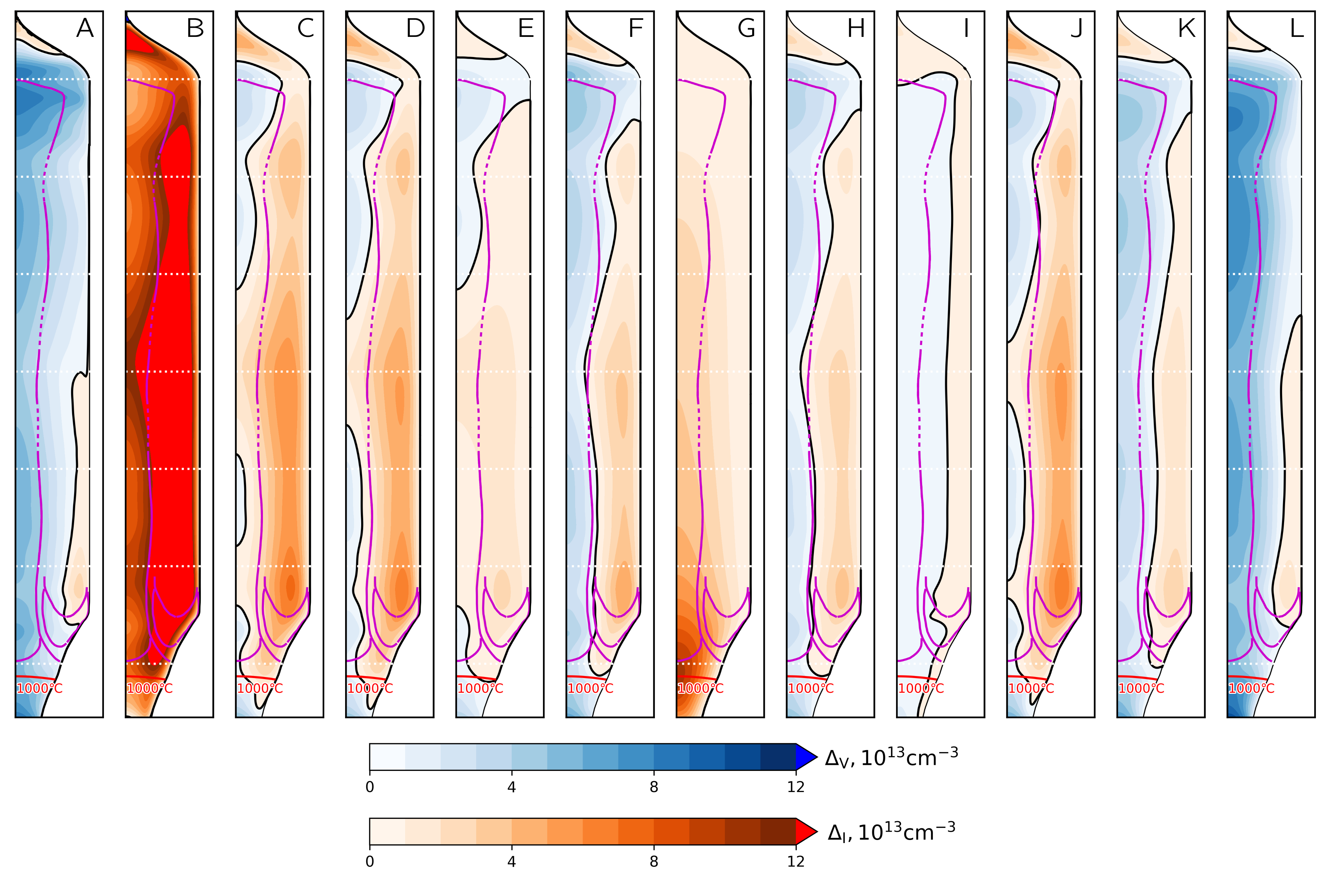
4.3.2. Original PD Parameters

The results with the original PD parameters summarized in Table 1 and Table 3 are depicted in Figure 5. The temperature of 1000 C below which the defects are frozen-in is located in the endcone, meaning that almost the whole crystal can be compared with the experiment.
Only a few PD parameter sets—F, H, I and K—produce reasonable results but none of them is perfect. For sets A and L the crystal center is too vacancy-rich and for the remaining sets too interstitial-rich. The prediction of the IVB during shouldering is especially difficult—its modeled axial position at r = 0 is typically too high.
These results qualitatively correspond to the theoretical ξ crit in Table 4 and modeled v / G curve in Figure 2. For example, neglecting the stress influence, a fully vacancy-rich center in the body phase is expected for parameter sets with ξ crit < 1.8   ×   10 3 c m 2 min 1 K 1 . The actual PD results suggest this value is around 1.45   ×   10 3 c m 2 min 1 K 1 (between sets E and H). Assuming a typical stress level of 20 M P a (sets K and L), the same tendencies are also observed for sets with the stress influence.
The thermal stress influence can be seen by comparing parameter set pairs C & J, and H & K, which have otherwise identical PD parameters: the IVB is shifted away from the axis and becomes straighter (i.e., having weaker radial variations), improving agreement with experiment.

4.3.3. Adjusted PD Parameters

To allow for a more direct comparison of all parameter sets and to improve agreement with experiment, all PD parameter sets were adjusted using quasi-stationary PD and thermal stress simulations on the temperature field obtained in the dynamic simulations. The equilibrium concentration of self-interstitials was adjusted by changing the formation entropy by Δ S I f , to match the experimentally observed I-V boundary at L = 600 mm. The corresponding scale factor for C I eq in Equation (5) is
C I eq scale = exp ( Δ S I f / k ) .
The reason why this approach works is that even small changes in C I eq considerably affect ξ crit (7) since the difference of two close values C V eq and C I eq is in the denominator. Table 4 provides a summary of the adjustments. Except for sets B and G, which originally had substantially higher ξ crit than the rest, the largest change of C I eq was only about 8%, therefore adjustment of the diffusivity to keep the same transport capacity was not performed.
Also shown in Table 4 is ξ crit for both the original and adjusted parameter sets. While ξ crit varies, a value of 1.32   ×   10 3 c m 2 min 1 K 1 is typical for adjusted cases both without and with a stress influence, which is more consistent, compared to the original PD parameters. As illustrated in Figure 6, after adjusting parameter sets with a stress influence, they are in a good agreement regarding ξ crit for compressive stresses around σ ave = 20 M P a . The different slopes for sets I and J are due to low C V eq C I eq and low d H V f / d σ , respectively.
Figure 7 shows the obtained PD distributions, which are now much more consistent and generally are in a better agreement with the experiment. There are two exceptions: set G could not reproduce the IVB in the cone and body phases due to too high C V (even for a higher ξ crit the IVB in the beginning of body phase is expected to be missing), and set I which, despite C I eq changes by only 1.3%, has an unrealistically strong stress influence on ξ crit (due to an order of magnitude lower C V eq C I eq , compared to other sets) (Figure 6) and a rather “flat” interstitial distribution with almost no vacancies. These sets will be omitted from further discussion.
As intended, the adjusted parameter sets predict the correct radial position of the IVB in the body phase at L = 600 mm. However, for all cases without the thermal stress influence, the IVB (i) was shifted away from the axis at other body phase positions and (ii) was not present in the shoulder region.
For set J with a thermal stress influence the agreement in the body phase is improved but the IVB is still absent at the shoulder. Finally, the best results are achieved by the two last sets with a stress influence—K and especially L—although some differences are still present in the shoulder and initial part of the body phase.
The thermal stress influence is crucial for the correct prediction of the IVB, as can be seen by comparing set pairs C & J, and H & K. As was already observed for the original PD parameters, the IVB becomes straighter, which is in a better agreement with experiment. A worse performance of set J, compared to K and L, is most likely due to weaker stress parameters, see Table 3 and Figure 4. We believe that adjustment of d H f / d σ can further improve agreement with the experiment, but such investigation is beyond the scope of this paper.
Since various authors use different thermophysical properties and modeling software in their heat transfer and PD simulations, the PD parameters were adjusted in the present study. The same global heat transfer was considered for all cases, allowing us to focus solely on the point defects. As a result, the differences between the adjusted PD parameter sets were rather small compared to the original ones, which could indicate their “universality”, as confirmed by a more consistent value of ξ crit in Table 4. The main takeaway is that the PD parameters alone are insufficient—they have to be considered in conjunction with the thermophysical parameters.
Although our simulations were based on a single experiment, a wide variety of thermal field and pull rate combinations occurred during the strongly transient full crystal growth, therefore we believe the adjusted model can be applied to other hot-zones and growth conditions. In future, it would be beneficial to validate the PD parameter sets against several crystals, especially of larger diameter, to fine-tune the parameters for thermal stress influence.

5. Conclusions

A detailed comparison of 12 published point defect parameter sets has been carried out for Cz growth of an industrial-size Si crystal. The PD defect distributions obtained by different parameter sets were very diverse and none was able to reproduce the experiment, therefore the parameters were adjusted. The IVB, especially at the shoulder and early body phase, could not be satisfactorily predicted by adjusted PD sets without the thermal stress influence. A good agreement with experiment was achieved only for parameter sets with the stress influence and sufficiently high formation enthalpy change. The contribution of an inaccurate heat transfer simulation to the observed discrepancy between the calculated and experimental IVB at the shouldering cannot be ruled out.

Author Contributions

Conceptualization, A.S. (Andrejs Sabanskis), M.P., A.S. (Andreas Sattler) and J.V.; methodology, A.S. (Andrejs Sabanskis), A.S. (Andreas Sattler) and J.V.; software, A.S. (Andrejs Sabanskis); validation, A.S. (Andrejs Sabanskis), M.P.; formal analysis, A.S. (Andrejs Sabanskis), M.P. and A.S. (Andreas Sattler); investigation, A.S. (Andrejs Sabanskis), M.P. and A.S. (Andreas Sattler); writing—original draft preparation, A.S. (Andrejs Sabanskis) and J.V.; writing—review and editing, M.P., A.S. (Andreas Sattler) and A.M.; visualization, A.S. (Andrejs Sabanskis), M.P.; supervision, A.S. (Andreas Sattler) and J.V.; funding acquisition, A.S. (Andrejs Sabanskis) and A.M. All authors have read and agreed to the published version of the manuscript.

Funding

A. Sabanskis acknowledges financial support from the PostDoc Latvia Project No. 1.1.1.2/VIAA/2/18/280.

Data Availability Statement

The data presented in this study are available within the article.

Conflicts of Interest

The authors declare no conflict of interest.

Abbreviations

The following abbreviations are used in this manuscript:
BCBoundary condition
FEMFinite element method
ISelf-interstitials
IVBI-V boundary
LPSLateral photovoltage scanning
MPMelting point
µ-PCDMicrowave photoconductivity decay
PDPoint defects
TPTriple point
VVacancies

References

  1. Voronkov, V.V. The mechanism of swirl defects formation in silicon. J. Cryst. Growth 1982, 59, 625–643. [Google Scholar] [CrossRef]
  2. Dornberger, E.; von Ammon, W. The dependence of ring-like distributed stacking faults on the axial temperature gradient of growing Czochralski silicon crystals. J. Electrochem. Soc. 1996, 143, 1648–1653. [Google Scholar] [CrossRef]
  3. Dornberger, E.; von Ammon, W.; Virbulis, J.; Hanna, B.; Sinno, T. Modeling of transient point defect dynamics in Czochralski silicon crystals. J. Cryst. Growth 2001, 230, 291–299. [Google Scholar] [CrossRef]
  4. Sinno, T.; Brown, R.A.; von Ammon, W.; Dornberger, E. Point defect dynamics and the oxidation-induced stacking-fault ring in Czochralski-grown silicon crystals. J. Electrochem. Soc. 1998, 145, 302–318. [Google Scholar] [CrossRef]
  5. Woo, H.S.; Jeong, J.H.; Kang, I.S. Optimization of surface temperature distribution for control of point defects in the silicon single crystal. J. Cryst. Growth 2003, 247, 320–332. [Google Scholar] [CrossRef]
  6. Dupret, F.; Nicodème, P.; Ryckmans, Y.; Wouters, P.; Crochet, M.J. Global modelling of heat transfer in crystal growth furnaces. Int. J. Heat Mass Transf. 1990, 33, 1849–1871. [Google Scholar] [CrossRef]
  7. Dornberger, E.; von Ammon, W.; den Bogaert, N.V.; Dupret, F. Transient computer simulation of a CZ crystal growth process. J. Cryst. Growth 1996, 166, 452–457. [Google Scholar] [CrossRef]
  8. Den Bogaert, N.V.; Dupret, F. Dynamic global simulation of the Czochralski process I. Principles of the method. J. Cryst. Growth 1997, 171, 65–76. [Google Scholar] [CrossRef]
  9. Brown, R.A.; Maroudas, D.; Sinno, T. Modelling point defect dynamics in the crystal growth of silicon. J. Cryst. Growth 1994, 137, 12–25. [Google Scholar] [CrossRef]
  10. Van Goethem, N.; de Potter, A.; Van den Bogaert, N.; Dupret, F. Dynamic prediction of point defects in Czochralski silicon growth. An attempt to reconcile experimental defect diffusion coefficients with the V/G criterion. J. Phys. Chem. Solids 2008, 69, 320–324. [Google Scholar] [CrossRef]
  11. Von Ammon, W.; Sattler, A.; Kissinger, G. Springer handbook of electronic and photonic materials. In Springer Handbook of Electronic and Photonic Materials; Kasap, S., Capper, P., Eds.; Springer International Publishing: Cham, Switzerland, 2017; Chapter 5. Defects in Monocrystalline Silicon; pp. 111–132. [Google Scholar] [CrossRef]
  12. Tanahashi, K.; Inoue, N. Non-equilibrium thermodynamic analysis on the behaviour of point defects in growing silicon crystals: Effects of stress. J. Mater. Sci. Mater. Electron. 1999, 10, 359–363. [Google Scholar] [CrossRef]
  13. Tanahashi, K.; Kikuchi, M.; Higashino, T.; Inoue, N.; Mizokawa, Y. Concentration of point defects in growing CZ silicon crystal under the internal stresses: Effects of impurity doping and thermal stress. Phys. B Condens. Matter 1999, 273-274, 493–496. [Google Scholar] [CrossRef]
  14. Sattler, A.; von Ammon, W.; Weber, M.; Haeckl, W.; Schmidt, H. Semiconductor Wafers of Silicon and Method for their Production. U.S. Patent 8,043,427, 25 October 2011. [Google Scholar]
  15. Vanhellemont, J. Intrinsic point defect incorporation in silicon single crystals grown from a melt, revisited. J. Appl. Phys. 2011, 110, 063519. [Google Scholar] [CrossRef]
  16. Vanhellemont, J. On the impact of stress on intrinsic defect formation during single crystal silicon growth. Phys. B Condens. Matter 2012, 407, 3009–3012. [Google Scholar] [CrossRef]
  17. Vanhellemont, J.; Kamiyama, E.; Sueoka, K. Silicon single crystal growth from a melt: On the impact of dopants on the v/G criterion. ECS J. Solid State Sci. Technol. 2013, 2, P166–P179. [Google Scholar] [CrossRef]
  18. Nakamura, K.; Suewaka, R.; Ko, B. Experimental study of the impact of stress on the point defect incorporation during silicon growth. ECS Solid State Lett. 2014, 3, N5–N7. [Google Scholar] [CrossRef]
  19. Sueoka, K.; Kamiyama, E.; Vanhellemont, J.; Nakamura, K. Impact of Plane Thermal Stress near the Melt/Solid Interface on the v/G Criterion for Defect-Free Large Diameter Single Crystal Si Growth. ECS Solid State Lett. 2014, 3, P69–P72. [Google Scholar] [CrossRef]
  20. Kamiyama, E.; Abe, Y.; Banba, H.; Saito, H.; Maeda, S.; Kuliev, A.; Iizuka, M.; Mukaiyama, Y.; Sueoka, K. Impact of anisotropic thermal stress on behavior of grown-in defects during Si crystal growth from a melt. ECS J. Solid State Sci. Technol. 2016, 5, P553–P555. [Google Scholar] [CrossRef]
  21. Mukaiyama, Y.; Sueoka, K.; Maeda, S.; Iizuka, M.; Mamedov, V.M. Numerical analysis of effect of thermal stress depending on pulling rate on behavior of intrinsic point defects in large-diameter Si crystal grown by Czochralski method. J. Cryst. Growth 2020, 531, 125334. [Google Scholar] [CrossRef]
  22. Sueoka, K.; Mukaiyama, Y.; Maeda, S.; Iizuka, M.; Mamedov, V.M. Computer simulation of concentration distribution of intrinsic point defect valid for all pulling conditions in large-diameter Czochralski Si crystal growth. ECS J. Solid State Sci. Technol. 2019, 8, P228–P238. [Google Scholar] [CrossRef]
  23. Suewaka, R.; Nakamura, K. Effect of thermal stress on point defect behavior during single crystal Si growth. Jpn. J. Appl. Phys. 2019, 59, 015502. [Google Scholar] [CrossRef]
  24. Brown, R.A.; Wang, Z.; Mori, T. Engineering analysis of microdefect formation during silicon crystal growth. J. Cryst. Growth 2001, 225, 97–109. [Google Scholar] [CrossRef]
  25. Kulkarni, M.S. Defect dynamics in the presence of oxygen in growing Czochralski silicon crystals. J. Cryst. Growth 2007, 303, 438–448. [Google Scholar] [CrossRef]
  26. Nishimoto, M.; Nakamura, K.; Hourai, M.; Ono, T.; Sugimura, W.; Motooka, T. Determination of physical properties for point defects during CZ silicon crystal growth by high-precision thermal simulations. J. Jpn. Inst. Met. Mater. 2011, 75, 657–664. [Google Scholar] [CrossRef]
  27. Sabanskis, A.; Bergfelds, K.; Muiznieks, A.; Schröck, T.; Krauze, A. Crystal shape 2D modeling for transient CZ silicon crystal growth. J. Cryst. Growth 2013, 377, 9–16. [Google Scholar] [CrossRef]
  28. Sabanskis, A.; Virbulis, J. Modelling of thermal field and point defect dynamics during silicon single crystal growth using CZ technique. J. Cryst. Growth 2019, 519, 7–13. [Google Scholar] [CrossRef]
  29. Abe, T.; Takahashi, T. Intrinsic point defect behavior in silicon crystals during growth from the melt: A model derived from experimental results. J. Cryst. Growth 2011, 334, 16–36. [Google Scholar] [CrossRef]
  30. Bergfelds, K.; Sabanskis, A.; Virbulis, J. Validation of mathematical model for CZ process using small-scale laboratory crystal growth furnace. IOP Conf. Ser. Mater. Sci. Eng. 2018, 355, 012004. [Google Scholar] [CrossRef]
  31. Arndt, D.; Bangerth, W.; Davydov, D.; Heister, T.; Heltai, L.; Kronbichler, M.; Maier, M.; Pelteret, J.P.; Turcksin, B.; Wells, D. The deal.II library, version 8.5. J. Numer. Math. 2017, 25, 137–145. [Google Scholar] [CrossRef]
  32. Geuzaine, C.; Remacle, J.F. Gmsh: A 3-D finite element mesh generator with built-in pre- and post-processing facilities. Int. J. Numer. Methods Eng. 2009, 79, 1309–1331. [Google Scholar] [CrossRef]
  33. Voronkov, V.V.; Falster, R. Gigantic uphill drift of vacancies and self-interstitials in silicon. Mater. Sci. Eng. B 2009, 159–160, 138–141. [Google Scholar] [CrossRef]
  34. Oh, H.J.; Wang, J.H.; Yoo, H.D. Comparison of numerical simulation and experiment for the OiSF-ring diameter in czochralski-grown silicon crystal. J. Korean Cryst. Growth Cryst. Technol. 2000, 10, 356–361. [Google Scholar]
  35. Wang, J.H.; Oh, H.J.; Yoo, H.D. Numerical analysis for the dynamics of the oxidation-induced stacking fault in czochralski-grown silicon crystals. Korean J. Chem. Eng. 2001, 18, 81–87. [Google Scholar] [CrossRef]
  36. Nakamura, K.; Saishoji, T.; Tomioka, J. Simulation of the point defect diffusion and growth condition for defect free Cz silicon crystal. Electrochem. Soc. Proc. 2002, PV 2002-2, 554–566. [Google Scholar]
  37. Vanhellemont, J.; Kamiyama, E.; Nakamura, K.; Śpiewak, P.; Sueoka, K. Impacts of thermal stress and doping on intrinsic point defect properties and clustering during single crystal silicon and germanium growth from a melt. J. Cryst. Growth 2017, 474, 96–103. [Google Scholar] [CrossRef]
  38. Dornberger, E. Prediction of OSF Ring Dynamics and Grown-In Voids in Czochralski Silicon Crystals. Ph.D. Thesis, Université Catholique de Louvain, Ottignies-Louvain-la-Neuve, Belgium, 1997. [Google Scholar] [CrossRef]
  39. Rudevics, A.; Muiznieks, A.; Riemann, H.; Luedge, A.; Ratnieks, G.; von Ammon, W. Numerical study and comparisons with experimental data for transient behaviour of phase boundaries during industrial FZ process for silicon crystal growth. J. Cryst. Growth 2005, 275, e561–e565. [Google Scholar] [CrossRef]
  40. Software Package CGSim. Available online: https://www.str-soft.com/software/cgsim/ (accessed on 12 March 2021).
  41. Nakamura, K.; Saishoji, T.; Tomioka, J. Simulation of point defect distributions in silicon crystals during melt-growth. J. Cryst. Growth 2000, 210, 49–53. [Google Scholar] [CrossRef]
  42. Kulkarni, M.S. Lateral incorporation of vacancies in Czochralski silicon crystals. J. Cryst. Growth 2008, 310, 3183–3191. [Google Scholar] [CrossRef]
  43. Sinno, T. A bottom-up multiscale view of point-defect aggregation in silicon. J. Cryst. Growth 2007, 303, 5–11. [Google Scholar] [CrossRef]
  44. Nishimoto, M.; Sueoka, K.; Motooka, T. First-principles calculation for interfacial energy of void defect in CZ silicon crystal. J. Jpn. Inst. Met. Mater. 2011, 75, 640–644. [Google Scholar] [CrossRef]
Figure 1. (a) Experimental µ-PCD measurements showing the IVB (part of data is mirrored to show the full crystal diameter) and (b) normalized crystal pull rate curve in the experiment and numerical simulations. The crystal length L is matched between (a,b); zero length corresponds to the beginning of the body phase, L < 0 is the cone (start cone).
Crystals 11 00460 g001
Figure 2. Calculated v / G ratio on the axis and at the triple point (TP, left axis) and calculated and experimentally measured crystallization interface deflection H C (right axis), defined as the vertical distance between the interface at TP and on the axis.
Crystals 11 00460 g002
Figure 3. Compilation of the calculated crystallization interface shapes plotted each 20 min. Also shown are the interfaces manually extracted from the experimental measurements (red dots). Dimensions are given in millimeters.
Crystals 11 00460 g003
Figure 4. Mean thermal stress σ ave (negative–compressive stresses shown with dashed isolines) for parameter sets I (left side), K and L (right side). In reading order: cone ( L = 50 mm); shouldering (0 mm); body phase (200 mm); body phase (1000 mm); endcone (1250 mm).
Crystals 11 00460 g004
Figure 5. Comparison of PD distributions with experimental IVB (solid magenta curves—measurements, dashed lines—interpolation) for original PD parameter sets (AL). Solid black curve— Δ = 0 , red curve— T = 1000   C below which PD are frozen-in, dotted white lines for length reference are plotted every 200 mm starting from L = 0 .
Crystals 11 00460 g005
Figure 6. The influence of thermal stress on ξ crit for original and adjusted PD parameter sets.
Crystals 11 00460 g006
Figure 7. Same as Figure 5, for adjusted PD parameter sets (AL).
Crystals 11 00460 g007
Table 1. Summary of considered point defect parameter sets defined by Equations (3)–(5). Suffix “-s” denotes parameter sets with the thermal stress influence, see Table 3 for the relevant parameters.
Parameter SetRef. D 0 ( cm 2 / s ) H m ( eV ) C 0 ( cm 3 ) H f ( eV ) Q ( eV )
A2000-Nakamura[41]I1.040 × 1042.41.060 × 10222.4
V2.1401.45.290 × 10222.6
B2001-Wang[34,35]I2.101 × 10−10.9073.945 × 10263.943−3.66
V1.000 × 10−40.4892.675 × 10232.848−2.66
C2002-Nakamura[36]I2.459 × 10−10.96.284 × 10264.05−1.01
V3.513 × 10−40.33.951 × 10263.940.0
D2007-Kulkarni-I[25,42]I1.950 × 10−10.96.176 × 10264
V6.262 × 10−40.47.520 × 10264
E2007-Kulkarni-II[25,42]I4.000 × 10−30.34.725 × 10274.3492
V2.000 × 10−30.381.200 × 10274.12
F2007-Sinno[43]I2.370 × 10−10.9376.365 × 10264.0
V7.870 × 10−40.4579.931 × 10253.7
G2009-Voronkov[33]I3.667 × 10−30.21.884 × 1094.954.5
V1.876 × 10−30.382.967 × 10263.9529
H2011-Nishimoto[26,44]I2.5901.185.992 × 10253.77
V9.918 × 10−40.41.400 × 10263.84
I2013-Vanhellemont-s[17]I3.800 × 10−20.886.400 × 10253.68
V1.200 × 10−30.452.580 × 10263.88
J2014-Nakamura-s[18]I2.459 × 10−10.96.284 × 10264.05−1.01
V3.513 × 10−40.33.951 × 10263.940.0
K2016-Kamiyama-s[20,26]I2.5901.185.992 × 10253.77
V9.918 × 10−40.41.400 × 10263.84
L2019-Mukaiyama-s[21,22]I2.459 × 10−10.96.284 × 10264.05
V3.442 × 10−40.34.030 × 10263.94
Table 2. Values of point defect parameters at the melting point.
Set D ( 10 4 cm 2 / s ) C eq ( 10 14 cm 3 ) C V eq C I eq DC eq ( 10 10 cm 1 s 1 )
IVIV ( 10 14 cm 3 ) IV
A6.8981.3907.0308.8501.81948.49512.303
B4.0700.0346.3488.1111.76225.8390.280
C5.0000.4454.8406.4901.65024.2002.888
D3.9640.3986.7128.1721.46126.6033.256
E5.0671.4604.6355.7071.07123.4898.334
F3.7340.3386.9178.5201.60225.8312.881
G9.2501.3702.9504.5501.60027.2886.234
H7.6560.6313.1744.5801.40624.3002.890
I0.8870.5416.3016.4070.1065.5873.467
J5.0000.4454.8406.4901.65024.2002.888
K7.6560.6313.1744.5801.40624.3002.890
L5.0000.4364.8406.6201.78024.2002.886
Table 3. Thermoelastic parameters (Young’s modulus E, coefficient of thermal expansion α , Poisson’s ratio ν ) at the MP and parameters for the thermal stress influence on the point defects d H f / d σ .
Parameter SetE α ν d H f d σ eV / GPa
( GPa ) ( 10 6 K 1 ) ( ) IV
I2013-Vanhellemont-s1004.660.25−0.0700.160
J2014-Nakamura-s139.74.660.225−0.0700.154
K2016-Kamiyama-s1664.660.217−0.06940.3069
L2019-Mukaiyama-s1654.660.217−0.06940.3069
Table 4. Adjustment of C I eq and the corresponding values of ξ crit (in 10 3 c m 2 min 1 K 1 ) at σ ave = 20 MPa for original and adjusted PD parameters.
Parameter Set Δ S I f / k C I eq Scale ξ crit orig. ξ crit adj.
A2000-Nakamura0.0371.0381.221.50
B2001-Wang−0.18020.8352.511.31
C2002-Nakamura−0.0560.9461.631.32
D2007-Kulkarni-I−0.03220.9681.571.32
E2007-Kulkarni-II−0.0310.9691.471.24
F2007-Sinno−0.00410.9961.351.32
G2009-Voronkov−0.66350.5152.321.23
H2011-Nishimoto−0.0140.9861.421.36
I2013-Vanhellemont-s0.01341.0130.600.85
J2014-Nakamura-s−0.03060.9701.451.29
K2016-Kamiyama-s0.03561.0361.201.35
L2019-Mukaiyama-s0.07951.0830.971.31
Publisher’s Note: MDPI stays neutral with regard to jurisdictional claims in published maps and institutional affiliations.

