Article

The Influence of Recrystallization on Zinc Oxide Microstructures Synthesized with Sol–Gel Method on Scintillating Properties

by
Ewelina Nowak
1,
Mirosław Szybowicz
1,*,
Alicja Stachowiak
2,
Daria Piechowiak
3,
Andrzej Miklaszewski
3,
Marcin E. Witkowski
4,
Michał Makowski
4,
Winicjusz Drozdowski
4,
Kazimierz Paprocki
5,*,
Kazimierz Fabisiak
5,
Szymon Łoś
6 and
Marek Trzcinski
6
1
Faculty of Materials Engineering and Technical Physics, Institute of Materials Research and Quantum Engineering, Poznań University of Technology, Piotrowo 3, 61-138 Poznań, Poland
2
Faculty of Materials Engineering and Technical Physics, Institute of Physics, Poznań University of Technology, Piotrowo 3, 61-138 Poznań, Poland
3
Faculty of Materials Engineering and Technical Physics, Institute of Materials Engineering, Poznań University of Technology, Piotrowo 3, 61-138 Poznań, Poland
4
Faculty of Physics, Astronomy, and Informatics, Institute of Physics, Nicolaus Copernicus University in Toruń, Grudziądzka 5/7, 87-100 Toruń, Poland
5
Institute of Physics, Kazimierz Wielki University, Jana Karola Chodkiewicza 30, 85-064 Bydgoszcz, Poland
6
Institute of Mathematics and Physics, UTP University of Science and Technology, Profesora Sylwestra Kaliskiego 7, 85-796 Bydgoszcz, Poland
*
Authors to whom correspondence should be addressed.
Submission received: 30 March 2021 / Revised: 28 April 2021 / Accepted: 5 May 2021 / Published: 11 May 2021
(This article belongs to the Special Issue Synthesis, Structure and Property Analysis of Crystalline Layers)

Abstract

:
Zinc oxide (ZnO) is one of the wide-bandgap semiconductors, which may be useful in a plethora of electronic, optical, piezoelectric, and scintillating applications. The following article consists in a structural and luminescence analysis of ZnO microfilms grown on a sapphire substrate with a sol–gel method. The films were annealed at different temperatures. The structures were investigated with the XRD and Raman methods, by which the influence of the substrate on the structure of the film was determined. The luminescence of films was investigated with room-temperature fluorescence, radioluminescence, and thermoluminescence.

1. Introduction

Over the last few decades, there has been a research renaissance in zinc oxide (ZnO)-based materials. ZnO is a group II-VI wide-bandgap semiconductor with a direct energy gap of around 3.4 eV. The material crystallizes preferentially in the hexagonal wurtzite-type structure [1,2]. Its large exciton binding energy of about 60 meV ensures an efficient excitonic emission at room temperature under low excitation energy [2,3].
This material occupies an extraordinary place among wide-bandgap semiconductors (such as GaN and ZnS) due to its properties. Increased demand for solid-state blue and UV light sources and detectors has led to functional studies of such compounds [4]. ZnO is considered an alternative to GaN for device applications due to its relatively low production cost and superior optical properties [5]. Thanks to the possibility of obtaining bulk crystals with a relatively high diameter and easy growth of epitaxial layers, quantum wells, nanorods, and related objects or quantum dots, ZnO is finding more and more applications in modern electronics [1]. Because it is colorless, the material may be used in transparent thin-film transistors (TFTs) [5] or as a transparent, highly conducting oxide (TCO) [1]. ZnO’s piezo- and pyroelectric properties allow its usage in sensors, converters, and energy generators [6]. The possibility of doping, e.g., with Co, Mn, or Fe, makes it suitable for spintronics [1]. Due to its hardness and rigidity, it is an essential material in the ceramics industry. The material is interesting for medicine and ecological systems due to its low toxicity, biocompatibility, and biodegradability [6]. Besides its attractive electrical and optical properties, ZnO is often considered a suitable material for ionizing radiation detectors. ZnO has sub-nanosecond decay times ascribed to free exciton emission, medium density (5.6 g/cm3), and potentially high light output [7]. In most cases, ZnO materials are modified to achieve new vacancies and defects in the structure, such as via doping with Cd, enhancing the scintillating properties [8].
Chemical stability and low-cost fabrication are some of the most significant advantages of ZnO [7]. The most usable form of the semiconductor—oriented ZnO films—may be grown with many different methods, such as MBE, pulsed laser deposition, metal-organic chemical vapor deposition, sputtering, spray pyrolysis, or electrodeposition [2,8]. However, sol–gel processes have been adapted to produce ZnO films in a low-cost, controlled, and simple way [9]. Sol–gel methods enable the obtainment of a solid material from a solution using a sol or a gel as an intermediate step. The synthesis involves wet chemistry reactions based on molecular precursors’ transformation into an oxide network by hydrolysis and condensation reactions [10]. Many ways of achieving ZnO thin films with a sol–gel technique have already been described in the literature [9,11,12,13,14,15]. The influence of the solvent, oxide precursor, substrate, or post-process treatment used has already been studied [9]. However, most previous studies focus on the properties of very thin layers. In this study, we prepared and characterized relatively thick ZnO films on a sapphire (Al2O3) {0001} substrate, which helps to understand the mechanism of lattice matching at a distance from the substrate concerning the changes in the annealing temperature. The structural changes may strongly influence the scintillating properties of each sample. Radioluminescence has already been extensively investigated for powder-type ZnO, high-quality thin films, or modified bulk crystals [7,8], but sol–gel-produced, non-doped ZnO microfilms still offer the possibility of development into an ionizing radiation sensor. Thus, the samples’ radiation response was also investigated as a part of their properties resulting from the structural changes.

2. Materials and Methods

2.1. Preparation of ZnO Films

As mentioned earlier, ZnO films were prepared with a sol–gel method. The precursor solution was synthesized by dissolving 2-hydrate zinc acetate powder in 2-metoxyethanol. The 1 molar solution was stabilized with diethanolamine. The prepared mixture was left for 1 h in an ultrasonic bath to achieve an entirely homogeneous consistency and annealed for 24 h at 50 °C to start the mechanism of condensation to achieve a sol.
The Al2O3 substrates were cleaned in four stages. The first step consisted of washing out the grease from a wafer with a detergent solution, followed by rinsing in MilliQ water. The next stage—cleaning in methanol—disposed of organic substances, which could have settled on the wafer during the first cleaning stage. The crystals were then bathed in a standard RCA-1, a process which is described elsewhere [16]. In the last step, wafers were rinsed in MilliQ water, cleaned one more time in acetone, and dried at 100 °C.
The films were deposited on substrates using a spin coater in two steps—with the rotation speed at 700 rpm for 30 s and 1000 rpm for 30 s. The division of the spinning process facilitates the obtainment of a homogenous film. The prepared films were heated at 120 °C for 5 min after each coating. For one of the samples, the coating-to-drying process was repeated 18 times, and for the other two samples, 50 times. The films were fired in an ambient atmosphere at 650, 800, and 1000 °C for 2 h. All samples were left in a furnace until they were completely cooled down.
Thorough sample information may be found in Table 1. The thickness of all samples was estimated by measuring the length of a cross-section under an optical microscope.

2.2. Instrumental Analysis

All of the films were synthesized from a precursor solution based on organic substances. Therefore, the investigation’s first step was to analyze one of the produced samples’ chemical composition. For this purpose, X-ray photoelectron spectroscopy (XPS) was used. The chemical state of Zn, O, and C, and their ratio were determined with a VG-Scienta R3000 hemispherical analyzer (ScientaOmicron, Uppsala, Sweden). Monochromatic Al K(α) radiation with an energy of 1486.6 eV was used as a source. The rules of Auger electron spectroscopy (AES) were used to assess excitation events resolved through secondary quantum numbers describing an electron’s total angular momentum in the atom.
The analysis’s main goal was to estimate the impact of the films’ structure on their physical properties. That is why the first part of the investigation was focused on morphology and crystal structure. Research began with evaluating the samples’ topography changes, which appeared under the influence of recrystallization. The crucial part of the analysis was to estimate the surface morphology of the analyzed samples. The overall topography was checked with a Zeiss LSM 710 confocal microscope (Zeiss Microscopy, Berlin, Germany).
The next step was to assay the structural character of the samples, both the surface and cross-section. The aim was to determine changes under the influence of recrystallization and any differences in the layer’s characteristics at a distance from the crystalline substrate. The crystallographic structure of samples was estimated with X-ray diffraction (XRD) analysis conducted using the Panalytical Empyrean (Malvern Panalytical, Malvern, UK) equipment with a copper anode (CuKα, 1.54 Å) at a Bragg–Brentano reflection mode configuration with 45 kV and 40 mA parameters. The measurement parameters were set up for 20°–90° with 15 s per step and 0.0167° in all cases. The changes between each sample were also estimated with Raman microscopy. Raman scattering was observed at room temperature using the Renishaw inVia system (Renishaw sp. z o.o., Warsaw, Poland). The spectrometer was equipped with a Leica confocal microscope—for all measurements, the long-distance objective with 50 times magnification and an Argon laser at 488 nm as excitation light source were used. Films were investigated in their growth surface and their cross-section, whereas the cross-section measurements were obtained after cutting samples in the middle.
Defect formation in the lattice of ZnO strongly impacts the electron states. Thus, the luminescence measurements provided valuable information about the inner structure of films. Photoluminescence measurements were performed at room temperature with a Hitachi F-4500 system with a xenon lamp as an excitation light source.
Radioluminescence (RL) spectra and low-temperature thermoluminescence (ltTL) glow curves were recorded with an Acton Research Corporation SpectraPro-500i (ARC Acton Research Corp, Greer, SC, USA) monochromator equipped with a Hamamatsu R928 photomultiplier (Hamamatsu, Tokai, Japan). A LakeShore 330 Temperature Controller (Lake Shore Cryotronics, Inc., Westerville, OH, USA), a closed-cycle APD Cryogenics He-cooler (Air Products, Allentown, PA, USA), and a rotary vacuum pump were used to stabilize and control the thermal conditions inside the sample chamber. An Inel XRG3500 (INEL, Stratham, NH, USA) X-ray generator (Cu-anode tube, 45 kV, 10 mA) was employed as an excitation source. RL spectra were measured at temperatures between 10 and 350 K under pressure below 10 mTr, starting at the highest and terminating at the lowest temperature to avoid any contribution from potential thermally induced processes. Glow curves were taken after a 10 min X-ray irradiation of the sample at 10 K, at a heating rate of about 0.15 K/s.
High-temperature thermoluminescence (htTL) was measured with a Mikrolab RA’04 Reader (Mikrolab, Cracow, Poland). With this equipment, it was possible to obtain glow curves at temperatures from 315 to 550 K at a 1 K/s heating rate.

3. Results

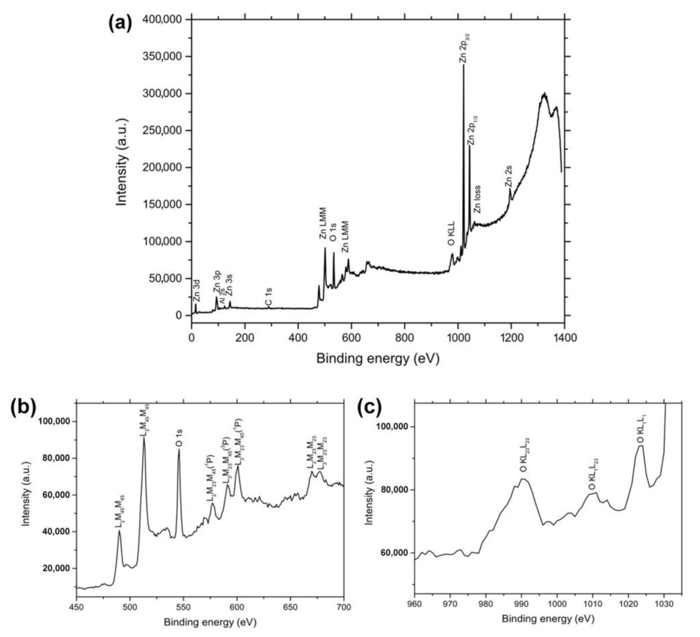
3.1. Chemical Composition of Samples

The first step in the layers’ investigation was the assessment of their chemical composition. ZnO layers were obtained from synthesis based on organic substances, which means that some organic residues could be embedded into the crystal lattice and act as carbon doping in obtained samples. Moreover, the samples were annealed in an oxygen-rich atmosphere, influencing the stoichiometry of the prepared structures. An X-ray photoelectron spectrum of one sample, 650_18, was measured to check the exemplary carbon and oxygen content. The spectra for the prominent peaks—Zn 2p3/2, O 1s, Al 2s, and C 1s—were measured 20 times, and the ratio of peaks for each spectrum was calculated and averaged (Figure 1). The estimated percentage composition of individual elements and uncertainty calculated according to Student’s t distribution with a 95% confidence interval are given in Table 2. As may be seen, the analyzed sample exhibits carbon contamination and relatively high oxygen content, which can be correlated with a non-controlled atmosphere during the annealing process.

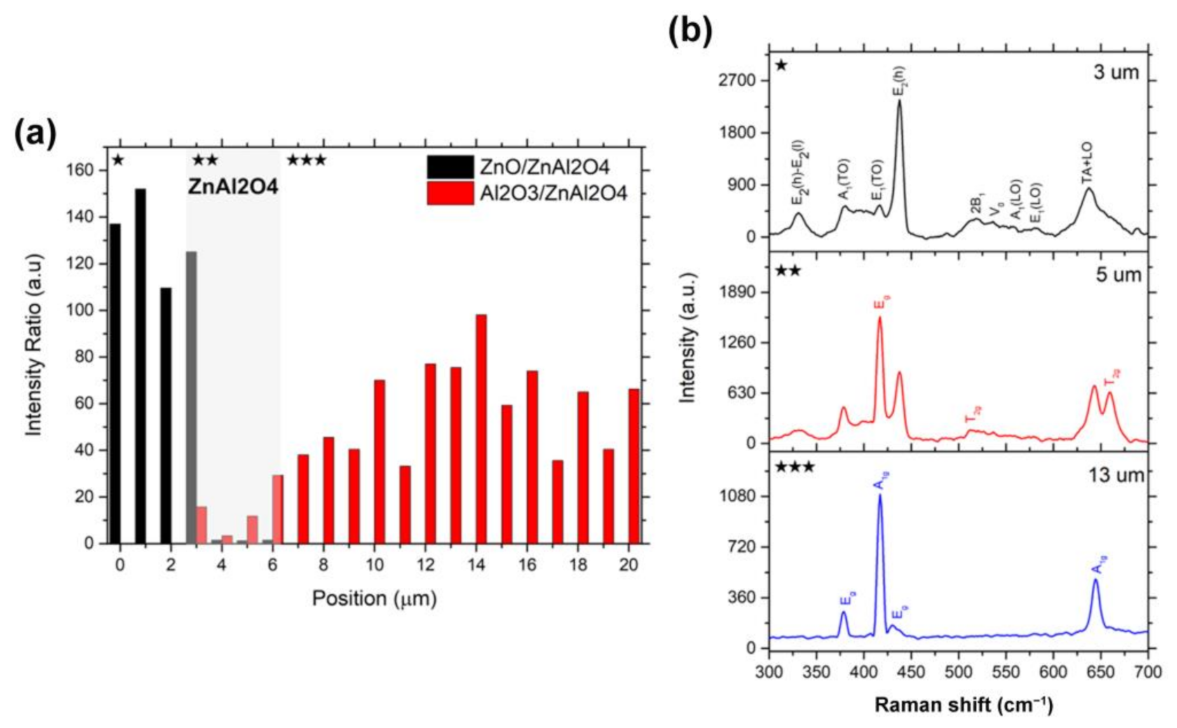
3.2. Topography and Structure

As mentioned earlier, samples were supplied with different amounts of thermal energy. This results in a completely different topography of their structure associated with different recrystallization and grain growth processes [19]. As can be seen in Figure 2, all of the samples exhibit small grains on their surface. What is more, most of the layers have visible, small pits on their surface—these pits appear due to the crumbling of the very brittle layer. Moreover, a film annealed at 1000 °C cracked under the influence of high temperature.
The distribution of grain size was measured for lengths of 3000 randomly selected microcrystals on each sample. All of the films show a considerable dispersion in crystallite length values. As may be seen, the distributions for samples fired at 800 and 1000 °C are quite similar. However, the film annealed at 800 °C has the highest amount of crystals in the range of 2–8 μm, and the sample annealed at the lowest temperature exhibits the most grains smaller than 1 μm. What is more, the samples vary in averaged values of crystals size, with the lowest value exhibited by sample 650_18 (1.34 ± 0.85 μm), the highest by 800_50 (1.66 ± 1.03 μm), and the middle value by 1000_50 (1.40 ± 0.79 μm). The values were estimated with the arithmetic mean, and the statistical error was calculated using the standard deviation.
The influence of annealing temperature on the ZnO structure is shown in the XDR pattern (Figure 3a). All of the analyzed films exhibit the wurtzite (P63mc) symmetry and a polycrystalline character.
Due to the process of annealing, one can observe the changing of preferred orientations. The film fired at 650 °C has a polycrystalline structure, with a (002) slightly preferred orientation. However, the intensity of (100) and (101) peaks is also firm, and it can be concluded that the structure has three preferred orientations. In the samples annealed at 800 °C, the intensity of (002) and (101) is even. At 1000 °C, crystallites exhibit substantial reorientation, with the (002) preferred orientation and the (100) and (101) strongly decreasing [20]. The ratios between the intensity of each of the prominent peaks concerning annealing temperature are included in Figure 3c [21].
The diffractogram for sample 1000_50 exhibits additional peaks assigned to the ZnAl2O4 phase [22]. ZnAl2O4 may act as an intermediate phase between the sapphire substrate and the ZnO layer. The same phase assignment is included in Figure 3b, showing the displacement of the most prominent peak position. As shown in Figure 3d, the changes in interatomic planes are quite similar. In the d100 and d101 peaks, one may see a slight increase in size with the annealing temperature, and for d002, a decrease during annealing at 800 °C and a slight increase at 1000 °C. The exact interatomic quantities are presented in Table 3.
The lattice constant was calculated from the peaks for which Miller index l = 0; the c-constant was calculated from peaks where indicators h, k = 0 [2]. Values were averaged, and the standard deviation was used for the measurement error determination. Table 4 contains a summary of all calculated lattice parameters.
Table 4. Calculated lattice constants for each sample.
Sample No.a (Å)Δa (Å)c (Å)Δc (Å)
650_183.24890.00075.20610.0012
800_503.24990.00075.20450.0009
1000_503.25070.00095.20520.0002
The comparative graphs for individual unit cell sizes are shown in Figure 4.
Figure 4. (a) A-constant of samples annealed at 650, 800, and 1000 °C; (b) c-constant of samples annealed at 650, 800, and 1000 °C; (c) c/a ratio of samples annealed at 650, 800, and 1000 °C.
Crystals 11 00533 g004
As shown in the graphs, the a-constant exhibits an almost linear dependence of the increase in size with increasing temperature. Therefore, it is possible to conclude that there is an influence of temperature increase on lattice growth in directions perpendicular to the c-axis. It is difficult to speak about the effect of heating on the c-constant value. As the temperature increases, the value drops, but it increases again for a sample heated at 1000 °C. This could be related to annealing temperature and an intermediate phase between the layer and the substrate. Changing the values of lattice parameters results in a significant change in the ratio of the c/a constants. Along with the annealing temperature, the parameter value decreases exponentially for investigated samples.
ZnO’s wurtzite structure with two formula units in the primitive cell increases optical-phonon modes classified as A1 + E1 + 2E2 + 2B1 [9]. The two nonpolar E2 modes (E2-Low and E2-High) are only Raman active, and the B1 modes are infrared and Raman inactive (silent modes). Furthermore, the A1 and the E1 modes are polar, and their vibrations polarize the unit cell. This polarization results in the creation of a long-range electrostatic field, which in turn splits the polar modes into longitudinal optical and transverse optical components. The Raman modes observed in a spectrum depending on the Raman selection rules consider the crystal orientation relative to the directions and polarization of the incoming and outgoing light [23]. The samples were analyzed on their growth surface and cross-sections, which enabled the registration of all of the sapphire (Al2O3) and ZnO-related peaks.
The chosen substrate, c-plane Al2O3, belongs to the D3d6 space group with two molecular Al2O3 groups per unit cell, with the irreducible representations for the optical modes:
2A1g + 2A1u + 3A2g + 2A2u + 5Eg + 4Eu
where vibrations with symmetry A1g and Eg are Raman active [24]. As shown in Figure 5, the most prominent peak for the c-plane and cross-section of sapphire is A1g localized at 418 cm−1. The {0001} plane also exhibits three Eg peaks localized at 432, 578, and 751 cm−1. The cross-section of the substrate shows mostly peaks at 378 cm−1 (Eg) and 645 cm−1 (A1g).
Despite the polycrystalline character of samples, the crystals orientate more or less according to the substrate’s c-axis, which may be seen in a comparison of ZnO growth surfaces’ and ZnO cross-sections’ spectra. The spectra of both samples vary for different orientations. The E2 (high) mode, localized at 437 cm−1, is the most prominent peak for growth surface spectra. These spectra also exhibit lower intensive E2 (high)-E2 (low) at 330 cm−1 and almost imperceptible A1(TO) and E1(TO) modes at 380 and 415 cm−1. Both samples also exhibit quasi-LO (q-LO) mode, which is the mixing mode created when ZnO’s growth axis is tilted at a specific angle [24]. The spectra for cross-sections have three most prominent peaks—the E2 (high), A1(TO), and E1(TO) samples annealed at 650 and 800 °C exhibit an additional, broad peak at about 578 cm−1, correlated with the oxygen vacancies. The peak disappears in the case of a sample fired at 1000 °C [25].
Figure 6 shows the position shifting of ZnO-related modes registered from the growth surface—the values were averaged from 20 different measurements conducted on distinct regions of samples. As may be seen, with the increasing firing temperature, the position of peaks is red-shifted. Thus, one may assume lattice expansion, which may be confirmed by the increase in the c/a ratio with increased annealing temperature.
Both growth surfaces and cross-sections exhibit second order of TO and LO modes. It is worth noting that the shifting of characteristic ZnO bands is not shifted. Thus, the films did not occur fitting to the substrate lattice, and they are not epitaxial.
The two additional modes at 646 and 662 cm−1 appear in the case of most of the registered spectra. These modes are not active for pure ZnO crystals. The mode at 662 cm−1 is correlated with the ZnAl2O4 subphase, which forms due to the diffusion of the zinc ions into the sapphire substrate. As shown in Figure 7, the distribution of the mentioned mode is heterogeneous and depends strongly on the annealing temperature, and appears most likely in sample 1000_50. Figure 8 shows the Raman spectra obtained from the cross-section of the sample annealed at 1000 °C. As may be seen, three phases were observed—ZnO phase, spinel phase (with the characteristic peak at 662 cm−1) [26], and sapphire phase. The ratio between the intensity of characteristic peaks of all phases enabled the estimation of the thickness of ZnAl2O4. Figure 8a shows the proportion of 437 cm−1 ZnO peaks to 662 cm−1 ZnAl2O4 peaks, and 417 cm−1 Al2O3 peaks to 662 cm−1 Al2O4 modes. The region of the lowest ratio values indicates the presence of a spinel subphase. Thus, the estimated thickness of ZnAl2O4 is calculated as 3 μm. However, due to the diffusion of zinc ions, the presence of a faint 662 cm−1 mode was also registered deeper in the substrate. Thus, the spinel layer may not be entirely homogenous.
The mode at 646 cm−1 appears for the films and substrate of 800_50 and 1000_50 samples and vanishes in sample 650_18. Thus, it may also be correlated with the formation of the ZnAl2O4 phase. Looking at ab initio calculations from the work of Manjón et al. [27,28], this may originate from a disorder-activated Raman scattering (DARS). This scattering is induced by the breakdown of the lattice’s translation symmetry caused by defects or impurities either because of the dopant nature or the growth conditions.
The peak at 646 cm−1 can be assigned to the TA+B1(high) second-order mode [28], and its appearance may originate both from the annealing conditions and the lattice mismatch between the ZnO and Al2O3.
Due to significant differences in this layer’s thickness, it was easy to obtain the A1g from sapphire localized at 418 cm−1. Figure 9 shows the map of the ratio of the intensity of the most prominent peak of the layer—E2 (high) mode and A1g sapphire mode.

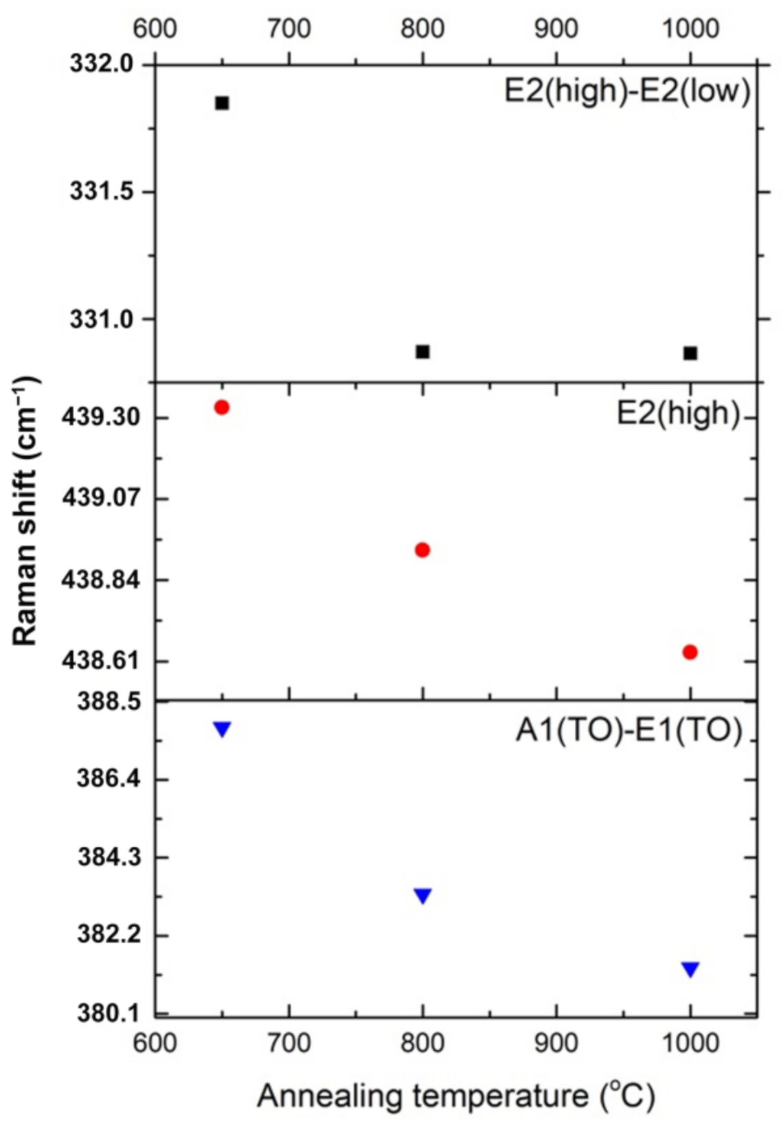
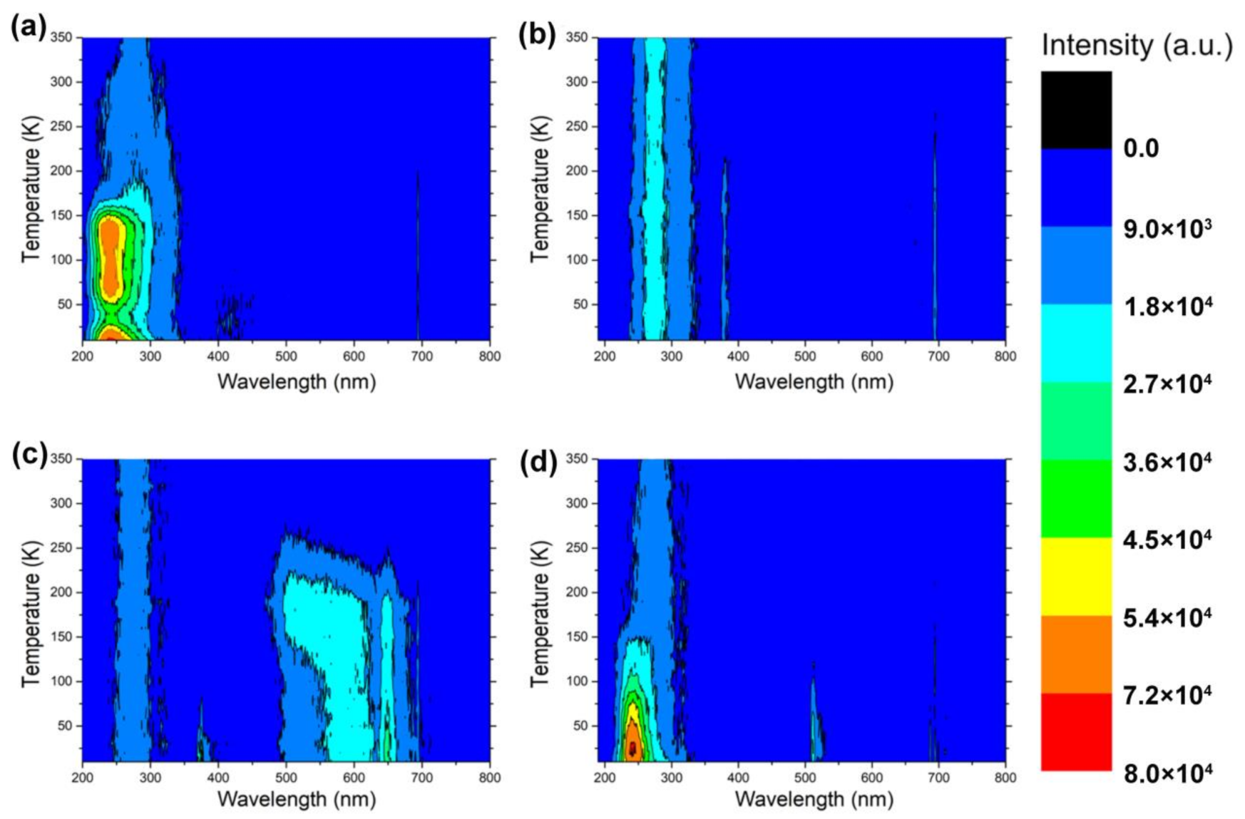
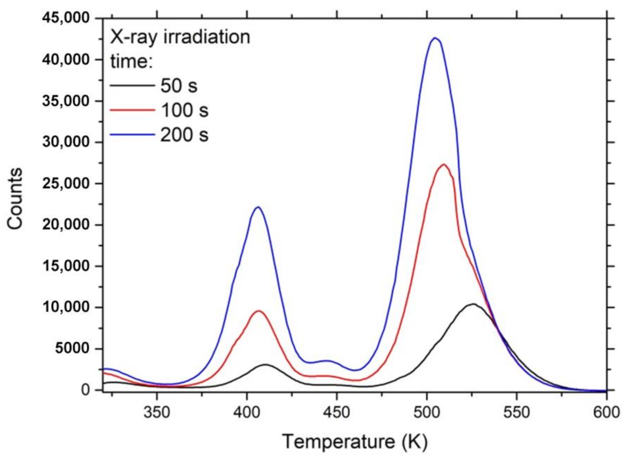
3.3. Luminescence Study

The study of luminescence provides valuable information on the purity and quality of the material. Figure 10 shows the room-temperature PL spectra of the ZnO layers. The PL measurements were conducted with 330 nm (3.75 eV) and 355 nm (3.49 eV) excitation. The PL spectra of ZnO at room temperature usually have two emission bands. One is in the UV region and is attributed to the near-band-edge emission through exciton–exciton collision processes. The other peak is in the visible region and presumably comes from the electron-hole recombination at a deep level (DL) emission in the bandgap caused by defects [29].
The luminescence intensity for a sample annealed at 650 °C is much lower than in the two other films, which can be correlated with its lower thickness. The band, assigned to near-band-edge emission dominated by donor-bound excitons [29], exhibits blue shifting with the increase in the annealing temperature (from 3.06 to 3.18 eV). Both 800_50 and 1000_50 samples exhibit two peaks at a region of 450–550 nm (2.25–2.75 eV). The wide green-band (2.6–2.75 eV) is attributed to a transition from the lower edge of the conduction band to the valence band’s upper edge [30]. The yellow luminescence, which is very intense in the case of the sample annealed at 800 °C, may be correlated with the hydrogen defects, which were already assigned by Reshchikov et al. [31]. As in the cited paper, the band was bleached in a sample annealed at higher temperatures. Because of the oxygen-rich atmosphere, one can also indicate that yellow luminescence originates from the transition between the conduction band and the energy levels formed with the substitution of O at Zn (OZn) vacancies [32].
The 2D radioluminescence maps are shown in Figure 11. A double-structured band peaking at 200–350 nm and a less intense narrow peak at 690 nm were observed in all samples. Both of these peaks come from a sapphire substrate and are not a subject of our investigation. The 650_18 layer exhibits an additional narrow peak at around 380 nm, which is characteristic of zinc oxide. This band can be assigned to excitonic luminescence [8,33]. A similar conclusion can be made about the weak broadband peaking at 650–800 nm, which may be correlated with defect-related emission [5,34]. For a more considerable amount of ZnO layers heated at 800 °C (800_50), those characteristic peaks start to dominate the RL spectrum, which is an expected effect. Unexpectedly for 1000_50, the band at 380 nm vanishes almost entirely, as in the infrared band. The wide band disappears, and a narrow peak with a remarkably small intensity remains. This narrow IR peak is probably also present in the 800_50 RL spectrum but cannot be detected due to its low intensity.
Figure 12 presents the low-temperature thermoluminescence results of all of the examined samples. The sapphire substrate reveals only one peak in the glow curve at around 240 K. For the remaining samples (except 1000_50), this peak is not detectable. We are aware that the ltTL glow curve of the 800_50 film looks very similar to the sapphire signal, but the 50 K shift of the peak is out of the question. Therefore, we conclude that we are dealing with a signal from a ZnO trap rather than a sapphire substrate trap. It can be propped up because this peak at around 300 K has also been detected for the 800_50 and 1000_50 samples. For the 800_50 film, intense broadband with an idle at about 40 K is observed, reduced for 1000_50 into two separate traps peaking at approximately 60 K and 140 K.
High-temperature thermoluminescence spectra are shown in Figure 13. All spectra have been obtained with a heating rate of 1 K/s after a 100 s X-ray irradiation and normalized to the peak at around 410 K. A brief analysis of gathered data leads to the conclusion that only one observed peak (with a maximum at approximately 525 K) comes from the sample itself. The rest of them come from the sapphire substrate. A comparison of the 800_50 and 1000_50 samples suggests that the increase in annealing temperature of the sample decreases the thermoluminescence signal from the ZnO layer, which may be correlated with the formation of the ZnAl2O4 subphase. Sample 1000_50 exhibits a broad peak at 425 K, which was also assigned previously [35] to oxygen ions in a spinel phase. For the 800_50 layer, htTL spectra with different irradiation times were recorded to analyze the order of kinetics (Figure 14). It can be seen (for both the sample and the substrate) that the maximum of each peak is not stable for different irradiation times, which means that we are not dealing with first-order traps [36].

4. Discussion

As mentioned earlier, all investigated samples were produced with a sol–gel method and annealed in an oxygen-rich atmosphere. Besides the temperature of annealing, samples vary in their thickness. Nevertheless, due to their high thickness and averaged grain sizes, the films do not exhibit nanostructure sizes. Therefore, the appearance of the quantum size effect can be considered improbable. As observed in Figure 2, samples consist of microcrystals, which vary enormously in shape and size. Thus, the strain and disorder on the film’s surface caused by production could lead to the formation of defects, such as dislocations and vacancy-type defects [37]. Samples vary in grain size and reorientation, indicating a thermally activated solid-phase mobility of the structure.
Diffusion processes of mass transfer between crystals occur during the firing of the film. This leads to the reorientation of crystals with the formation of the preferred direction (002) under the influence of the crystal field of the substrate. The formation and interaction of defects, influenced by impurities and annealing environment, already occur in samples fired at 650 and 800 °C. What is more, a firing temperature of about 1000 °C supplies enough thermal energy for zinc ions to diffuse into the substrate, which results in ZnAl2O4 phase formation [37]. XPS data indicated the presence of carbon contamination and high oxidation of the 650_18 sample. Therefore, the process of synthesis and deposition and the annealing lead to the appearance of imperfections in the lattice, which can significantly affect the sample’s properties. The best feature to estimate the layers’ quality may be the c/a ratio calculated by XRD measurements (Figure 4c).
Along with the annealing temperature, the parameter value decreases exponentially for investigated samples. The results suggest that the sintering crystals may be less compressed in the c-axis direction than in the other ranges (with the ideal c/a ratio = 1.633 for a hexagonal unit cell [2]). Since the c/a ratio also correlates with the difference in the two constituents’ electronegativities, components with the most significant differences show the most considerable departure from the ideal c/a ratio [2]. In the case of ZnO, this equals 1.6021 [38,39]. Higher c/a ratio average values for the obtained compacts compared with the base-rod material could be explained independently by inserting interstitial atoms with a smaller atom radius than that of zinc and oxygen [40]. As shown in the luminescence studies (Figure 10), samples annealed at higher temperatures exhibit yellow-green luminescence. The emission could be assigned to the transition between the conduction band and the energy levels formed with substitution of O at Zn (OZn) vacancies, which may lower the c/a ratio.
The sample annealed at the highest temperature exhibits diffraction peaks correlated with a subphase between the substrate and ZnO layer. This feature may implicate the appearance of additional dislocations associated with the lattice mismatch. The lattice mismatch, defects, and unintentional doping result in additional, disorder-activated Raman scattering bands. The peak localized at 662 cm−1 exhibits the most significant relative intensity in sample 1000_50 and is directly assigned to the spinel phase. Thus, the influence of the substrate-layer reaction is visible here.
Exposure of thermally stimulated phosphor materials to radiation creates electron-hole pairs that eventually become trapped in localized trap-states existing inside the material’s bandgap. Most of the charge carriers remain trapped afterward. The localized trap states in a material are generated due to the existing intrinsic defects or the defects generated by radiation exposure. The charge trapping and thermally stimulated recombination mechanisms are essential for radiation dose assessment. In a decent dosimetric material, the number of trapped charge carriers and the integrated intensity of the thermally stimulated light emission recombination are proportional to the exposure dose [41]. In the case of the analyzed samples, low- and high-temperature thermoluminescence studies were conducted. In ltTL, the samples varied with the characteristic of glow curves. Sample 650_18 exhibits a prominent curve at 300 K, and the same peak appears for sample 800_50. This feature may be correlated with the activation of the Zn2+i defect [42]; the interstitial atom may explain the higher c/a ratio calculated for sample 650_18.
Sample 800_50’s prominent peak at 150 K has been previously observed in various research studies. Ji [43] assigned a peak to hydrogen at a bound-centered lattice site donor type. The peak appeared for a crystal sample, which was annealed in a hydrogen and oxygen atmosphere. Isik et al. [44] observed similar characteristics for AZO nanoparticles, which may lead to inclination. The Al doping may be observed on the sample. The 1000_50 film exhibited a glow curve with a maximum at 80 K. A similar curve was also observed in [45] in a study on nanostructures; the work hypothesizes that for this peak (with activation energy calculated for 30 meV), the donor level may be identified as a Zn sublattice defect.
In the case of htTL, all samples exhibit a prominent peak at 525 K. The peak was observed in the case of ZnO sintered at 950 °C and shifted with the lowering of annealing temperature [46]. A similar characteristic was observed for ZnO pellets by Cruz-Vázquez et al. [47]. The peak may likely originate from zinc and oxygen vacancies [43], likely due to photoluminescence studies.
It is worth noting that RL, TL, and PL studies, and XRD and Raman spectroscopy indicate a substantial defect of the samples. Thus, it is possible to indicate a general conclusion that the sintering may fine-tune the dosimetric properties of ZnO microfilms. However, due to a limited amount of studied material, it is difficult to draw statistically unambiguous conclusions without comparing with other obtained results in the literature.

5. Conclusions

This work presents a detailed analysis of thick ZnO film structures, which may find application in dosimetry. The main aim of this research was to compare the structural and optical properties of ZnO samples prepared with the sol–gel method, which were annealed in different conditions.
Investigated samples were produced from an organic-based solution. The XPS measurements revealed that the investigated films contain a low concentration of carbon, which may act as an unintentional dopant—the appearance of carbon may be one reason for the formation of peaks induced by an additional strain in the lattice. What is more, carbon impurity is the reason for the increased formation of defects such as oxygen vacancies and lattice imperfections, which influence the spectroscopic signal of samples.
The structure of samples strongly depends on the temperature and time of annealing. Polycrystalline films exhibited reorientation of grains under changing annealing conditions. This issue was easily visible in confocal microscopy images. What is more, the reorientation of crystals was also proved by the Raman scattering. The increase in grain size during annealing indicates a redistribution of mass between crystals due to the thermal activation of solid-phase mobility. Thus, mobility leads to the reorientation of crystals to the preferred direction of (002) under the influence of the crystal field of the substrate.
Due to the thickness of the films, Raman spectroscopy enabled us to investigate the lattice changes at different distances from substrates. As could be seen on the sample cross-section spectra, bands from ZnO and the substrate were observed. It is worth noting that band shifting was not observed, which indicates that it was impossible to achieve even partial epitaxy. However, the XRD pattern for sample 1000_50 shows intermediate phase formation between sapphire and ZnO, which indicates thermally induced diffusion of zinc ions onto the Al2O3 crystal.
Samples exhibited DARS peaks on their surface, which may implicate the appearance of additional stresses resulting from imperfections in the crystal lattice. Due to the heterogeneous structure, the Raman spectra of sample 1000_50 enable detection of substrate peaks’ intensity changes.
The luminescence studies show that all of the structures exhibit substantial internal defects, which influence the emission. The photoluminescence was strongly influenced by the thickness and annealing temperature of each sample. This feature was readily observed in the prominent peaks, where the intensity of the 650_18 film was low. Moreover, the sample annealed at 800 °C exhibited strong yellow luminescence, which may be linked to hydrogen or oxygen defects.
The radioluminescence of each sample consists of two components. One is a signal from the sample substrate, while the other one is a signal originating from the ZnO layers. As expected, the higher the amount of layers on a substrate, the higher the sample-to-substrate RL signal ratio. It can also be observed that annealing at 1000 °C changes the sample RL spectrum. Thermoluminescence measurements showed interesting features, such as quenching of the htTL ZnO trap signal for a sample heated at a high temperature.

Author Contributions

Conceptualization, E.N. and M.S.; methodology, E.N., M.S., A.S., D.P., M.E.W., and M.M.; validation, M.S., A.M., W.D., M.T., K.P., and K.F.; formal analysis, E.N.; investigation, E.N., D.P., A.S., S.Ł., and M.T.; resources, E.N.; data curation, E.N., M.S., A.M., W.D., M.T., and K.P.; writing—original draft preparation, E.N.; writing—review and editing, M.S., D.P., A.S., A.M., M.E.W., M.M., W.D., M.T., K.P., K.F., and S.Ł.; visualization, E.N.; supervision, M.S.; project administration, E.N. and M.S.; funding acquisition, E.N. and M.S. All authors have read and agreed to the published version of the manuscript.

Funding

This research was funded by the Ministry of Science and Higher Education, grant number 0511/SBAD/0018 and 0512/SBAD/2120 for the year 2021.

Institutional Review Board Statement

This research did not require testing on animals or humans.

Informed Consent Statement

The research didn’t involve the experiments on humans and other living beings.

Data Availability Statement

We are able to deliver analyzed data via e-mail (the request may be send to: [email protected]).

Conflicts of Interest

The authors declare no conflict of interest. The funders had no role in the design of the study; in the collection, analyses, or interpretation of data; in the writing of the manuscript, or in the decision to publish the results.

Abbreviations

ZnOzinc oxide
XRDX-ray diffraction
Egenergy gap
MBEmolecular beam epitaxy
XPSX-ray photoelectron spectroscopy
AESAuger electron spectroscopy
PLphotoluminescence
RLradioluminescence
ltTLlow-temperature thermoluminescence
htTLhigh-temperature thermoluminescence

References

  1. Klingshirn, C.F. ZnO: Material, physics and applications. ChemPhysChem 2007, 8, 782–803. [Google Scholar] [CrossRef]
  2. Özgür, Ü.; Alivov, Y.I.; Liu, C.; Teke, A.; Reshchikov, M.; Doğan, S.; Avrutin, V.; Cho, S.-J. Morkoç, A comprehensive review of ZnO materials and devices. J. Appl. Phys. 2005, 98, 041301. [Google Scholar] [CrossRef] [Green Version]
  3. Mahendran, R.; Kashif, M.; Saroja, M.; Venkatachalam, M.; Sanjeeviraja, C.; Hashim, U. Structural and optical characterization of ZnO thin films annealed at different temperatures. J. Appl. Sci. Res. 2013, 9, 5460–5467. [Google Scholar]
  4. Rodnyi, P.; Khodyuk, I. Optical and luminescence properties of zinc oxide. Opt. Spectrosc. 2011, 111, 776–785. [Google Scholar] [CrossRef] [Green Version]
  5. Özgür, Ü.; Hofstetter, D.; Morkoç, H. ZnO Devices and Applications: A Review of Current Status and Future Prospects. Proc. IEEE 2010, 98, 1255–1268. [Google Scholar] [CrossRef]
  6. Kołodziejczak-Radzimska, A.; Jesionowski, T. Zinc oxide-from synthesis to application: A review. Materials 2014, 7, 2833–2881. [Google Scholar] [CrossRef] [Green Version]
  7. Yanagida, T.; Fujimoto, Y.; Yamanoi, K.; Kano, M.; Wakamiya, A.; Kurosawa, S.; Sarukura, N. Optical and scintillation properties of bulk ZnO crystal. Phys. Status Solidi C 2012, 9, 2284–2287. [Google Scholar] [CrossRef]
  8. Ismail, A.; Al Abdullah, J.; Shweikani, R.; Jerby, B. Radioluminescence in ZnO: Effect of chemical modification. J. Optoelectron. Adv. Mater. 2017, 19, 389–394. [Google Scholar]
  9. Znaidi, L. Sol–gel-deposited ZnO thin films: A review. Mater. Sci. Eng. B 2010, 174, 18–30. [Google Scholar] [CrossRef]
  10. Hasuike, N.; Harada, T.; Kiyohara, T.; Nishio, K.; Kisoda, K.; Harima, H. Low temperature synthesis of ZnO thin films by spin—coating technique. Phys. Status Solidi C 2011, 8, 506–508. [Google Scholar] [CrossRef]
  11. Zawadzka, A.; Płóciennik, P.; Strzelecki, J.; Sahraoui, B. Transparent amorphous zinc oxide thin films for NLO applications. Opt. Mater. 2014, 37, 327–337. [Google Scholar] [CrossRef] [Green Version]
  12. Kim, S.; Yoon, H.; Kim, S.-O.; Leem, J.-Y. Optical properties and electrical resistivity of boron-doped ZnO thin films grown by sol–gel dip-coating method. Opt. Mater. 2013, 35, 2418–2424. [Google Scholar] [CrossRef]
  13. Bala, W.; Zorenko, Y.; Savchyn, V.; Voznyak, T.; Paprocki, K.; Popielarski, P.; Szybowicz, M. Optical and electrical properties of ZnO thin films grown by sol-gel method. Solid State Phenom. 2013, 200, 14–21. [Google Scholar] [CrossRef]
  14. Znaidi, L.; Touam, T.; Vrel, D.; Souded, N.; Ben Yahia, S.; Brinza, O.; Fischer, A.; Boudrioua, A. ZnO thin films synthesized by sol-gel process for photonic applications. Acta Phys. Pol. A 2012, 121, 165–168. [Google Scholar] [CrossRef]
  15. Sahal, M.; Hartiti, B.; Ridah, A.; Mollar, M.; Mari, B. Structural, electrical and optical properties of ZnO thin films deposited by sol–gel method. Microelectron. J. 2008, 39, 1425–1428. [Google Scholar] [CrossRef]
  16. Bachman, M. Cleaning Procedures for Silicon Wafers; University of California Irvine: Irvine, CA, USA, 2002. [Google Scholar]
  17. Moulder, J.F.; Stickle, W.F.; Sobol, P.E.; Bomben, K.D. Handbook of X-ray Photoelectron Spectroscopy; Perkin-Elmer Corporation: Eden Prairie, MN, USA, 1992. [Google Scholar]
  18. Jenkins, R.; Manne, R.; Robin, R.; Senemaud, C. Nomenclature, symbols, units and their usage in spectrochemical analysis-VIII. Nomenclature system for X-ray spectroscopy (Recommendations 1991). Pure Appl. Chem. 1991, 63, 735–746. [Google Scholar] [CrossRef]
  19. Haško, D.; Bruncko, J.; Uherek, F. Surface morphology study of recrystallization dynamics of amorphous ZnO layers prepared on different substrates. Appl. Phys. A 2014, 117, 1353–1358. [Google Scholar] [CrossRef]
  20. Albertsson, J.; Abrahams, S.C.; Kvick, A. Structure and properties (Liquid crystals, polymers, glasses, etc.). Z. Kristallogr. Cryst. Mater. 1988, 185, 526. [Google Scholar] [CrossRef]
  21. Sowa, H.; Ahsbahs, H. High-pressure X-ray investigation of zincite ZnO single crystals using diamond anvils with an improved shape. J. Appl. Crystallogr. 2006, 39, 169–175. [Google Scholar] [CrossRef]
  22. Levy, D.; Pavese, A.; Sani, A.; Pischedda, V. Structure and compressibility of synthetic ZnAl2O4 (gahnite) under high-pressure conditions, from synchrotron X-ray powder diffraction. Phys. Chem. Miner. 2001, 28, 612–618. [Google Scholar] [CrossRef]
  23. Bergman, L.; Chen, X.-B.; Huso, J.; Morrison, J.L.; Hoeck, H. Raman scattering of polar modes of ZnO crystallites. J. Appl. Phys. 2005, 98, 093507. [Google Scholar] [CrossRef]
  24. Porto, S.P.S.; Krishnan, R.S. Raman effect of corundum. J. Chem. Phys. 1967, 47, 1009–1012. [Google Scholar] [CrossRef]
  25. Jabri, S.; Souissi, H.; Souissi, A.; Meftah, A.; Sallet, V.; Lusson, A.; Galtier, P.; Oueslati, M. Investigation of the vibrational modes of ZnO grown by MOCVD on different orientation planes. J. Raman Spectrosc. 2015, 46, 251–255. [Google Scholar] [CrossRef]
  26. Mohaček-Grošev, V.; Vrankić, M.; Maksimović, A.; Mandić, V. Influence of titanium doping on the Raman spectra of nanocrystalline ZnAl2O4. J. Alloys Compd. 2017, 697, 90–95. [Google Scholar] [CrossRef]
  27. Manjón, F.; Mari, B.; Serrano, J.; Romero, A. Silent Raman modes in zinc oxide and related nitrides. J. Appl. Phys. 2005, 97, 053516. [Google Scholar] [CrossRef] [Green Version]
  28. Song, Y.; Zhang, S.; Zhang, C.; Yang, Y.; Lv, K. Raman spectra and microstructure of zinc oxide irradiated with swift heavy ion. Crystals 2019, 9, 395. [Google Scholar] [CrossRef] [Green Version]
  29. Cuscó, R.; Alarcón-Lladó, E.; Ibanez, J.; Artús, L.; Jiménez, J.; Wang, B.; Callahan, M.J. Temperature dependence of Raman scattering in ZnO. Phys. Rev. B 2007, 75, 165202. [Google Scholar] [CrossRef]
  30. Raoufi, D. Synthesis and photoluminescence characterization of ZnO nanoparticles. J. Lumin. 2013, 134, 213–219. [Google Scholar] [CrossRef]
  31. Reshchikov, M.; Moon, Y.; Gu, X.; Nemeth, B.; Nause, J.; Morkoç, H. Unstable luminescence in GaN and ZnO. Phys. B 2006, 376, 715–718. [Google Scholar] [CrossRef]
  32. Verma, D.; Kole, A.; Kumbhakar, P. Red shift of the band-edge photoluminescence emission and effects of annealing and capping agent on structural and optical properties of ZnO nanoparticles. J. Alloys Compd. 2015, 625, 122–130. [Google Scholar] [CrossRef]
  33. Grigorjeva, L.; Zolotarjovs, A.; Sokovnin, S.Y.; Millers, D.; Smits, K.; Ilves, V.G. Radioluminescence, thermoluminescence and dosimetric properties of ZnO ceramics. Ceram. Int. 2017, 43, 6187–6191. [Google Scholar] [CrossRef]
  34. Buryi, M.; Babin, V.; Chang, Y.-Y.; Remeš, Z.; Mičová, J.; Šimek, D. Influence of precursor age on defect states in ZnO nanorods. Appl. Surf. Sci. 2020, 525, 146448. [Google Scholar] [CrossRef]
  35. Jain, M.; Kumar, R.; Won, S.O.; Chae, K.H.; Vij, A.; Thakur, A. Defect states and kinetic parameter analysis of ZnAl2O4 nanocrystals by X-ray photoelectron spectroscopy and thermoluminescence. Sci. Rep. 2020, 10, 1–14. [Google Scholar] [CrossRef]
  36. Bos, A.; Dielhof, J. The analysis of thermoluminescent glow peaks in CaF2: Tm (TLD-300). Radiat. Prot. Dosim. 1991, 37, 231–239. [Google Scholar] [CrossRef] [Green Version]
  37. Sendi, R.K.; Mahmud, S. Quantum size effect on ZnO nanoparticle-based discs synthesized by mechanical milling. Appl. Surf. Sci. 2012, 258, 8026–8031. [Google Scholar] [CrossRef]
  38. Kisi, E.H.; Elcombe, M.M. u parameters for the wurtzite structure of ZnS and ZnO using powder neutron diffraction. Acta Crystallogr. Sect. C Cryst. Struct. Commun. 1989, 45, 1867–1870. [Google Scholar] [CrossRef]
  39. Branson, D.L. Kinetics and mechanism of the reaction between zinc oxide and aluminum oxide. J. Am. Ceram. Soc. 1965, 48, 591–595. [Google Scholar] [CrossRef]
  40. Miklaszewski, A.; Garbiec, D.; Niespodziana, K. Sintering behavior and microstructure evolution in cp-titanium processed by spark plasma sintering. Adv. Powder Technol. 2018, 29, 50–57. [Google Scholar] [CrossRef]
  41. Pal, U.; Meléndrez, R.; Chernov, V.; Barboza-Flores, M. Thermoluminescence properties of ZnO and ZnO:Yb nanophosphors. Appl. Phys. Lett. 2006, 89, 183118. [Google Scholar] [CrossRef]
  42. Epie, E.N.; Chu, W.K. Ionoluminescence study of Zn− and O− implanted ZnO crystals: An additional perspective. Appl. Surf. Sci. 2016, 371, 28–34. [Google Scholar] [CrossRef]
  43. Ji, J. Donors and Defects Characterization in ZnO by Luminescence Techniques; Washington State University: Pullman, WA, USA, 2015. [Google Scholar]
  44. Isik, M.; Gasanly, N.M. Thermoluminescence properties of Al doped ZnO nanoparticles. Ceram. Int. 2018, 44, 13929–13933. [Google Scholar] [CrossRef]
  45. Isik, M.; Yildirim, T.; Gasanly, N.M. Thermoluminescence properties of ZnO nanoparticles in the temperature range 10–300 K. J. Sol-Gel Sci. Technol. 2016, 78, 76–81. [Google Scholar] [CrossRef]
  46. Borbón-Nuñez, H.; Cruz-Vázquez, C.; Bernal, R.; Kitis, G.; Furetta, C.; Castaño, V. Thermoluminescence properties of sintered ZnO. Opt. Mater. 2014, 37, 398–403. [Google Scholar] [CrossRef]
  47. Cruz-Vázquez, C.; Borbón-Nuñez, H.A.; Orante-Barrón, V.R.; Burruel-Ibarra, S.E.; Castaño, V.M.; Bernal, R. Synthesis and Thermoluminescence of New ZnO Phosphors. MRS Online Proc. Library 2011, 1278, 8. [Google Scholar] [CrossRef]
Figure 1. XPS and AES spectra for sample 650_18 excited with Al K(α) radiation with 1486.6 eV of energy: (a) XPS widescan; (b) Auger lines of zinc; (c) Auger lines of oxygen. AES peaks follow IUPAC notation in which the transition between the initial and final states occurs [17,18].
Crystals 11 00533 g001
Figure 2. Micrographs made with confocal microscopy in material mode and distribution of crystallite size.
Crystals 11 00533 g002
Figure 3. (a) XRD patterns of samples annealed at 650, 800, and 1000 °C; (b) XRD patterns of each sample in a shorter range with the designation of another observed phase; (c) the ratio of intensity between the most prominent peaks; (d) the shifting of the most prominent peaks.
Crystals 11 00533 g003
Figure 5. Raman spectra for substrate and ZnO films (on growth surface and cross-section) registered for different annealing temperatures: (a) 650 °C, (b) 800 °C, and (c) 1000 °C. ZnO peaks are marked with a gray dotted line; Al2O3 peaks are marked with a gray rectangle.
Crystals 11 00533 g005
Figure 6. Raman shifting of the most prominent modes of ZnO films registered for different annealing temperatures.
Crystals 11 00533 g006
Figure 7. Maps of the ratio of the intensity of E2(high) and 662 cm−1 mode: (a) 650 °C, (b) 800 °C, and (c) 1000 °C.
Crystals 11 00533 g007
Figure 8. Cross-section data of sample 1000_50: (a) estimation of the thickness of the ZnAl2O4 phase due to the ratio of intensities of ZnO and ZnAl2O4, and Al2O3 and ZnAl2O4 modes; (b) the spectra in different registered positions at 3 μm (the ZnO phase), 5 μm (the spinel phase), and 13 μm (Al2O3 phase).
Crystals 11 00533 g008
Figure 9. Map of the ratio of the intensity of E2 (high)–ZnO related peak to A1g–Al2O3 pertaining peak.
Crystals 11 00533 g009
Figure 10. The photoluminescence of: (a) all samples measured with a 330 nm excitation; (b) sample 650_18 measured with a 330 nm excitation; (c) samples 800_50 and 1000_50 measured with a 355 nm excitation.
Crystals 11 00533 g010
Figure 11. 2D radioluminescence maps of (a) the sapphire substrate, (b) 650_18 sample, (c) 800_50 sample, and (d) 1000_50 sample.
Crystals 11 00533 g011
Figure 12. Low-temperature thermoluminescence of sapphire substrate, 650_18 sample, 800_50 sample, and 1000_50 sample.
Crystals 11 00533 g012
Figure 13. High-temperature thermoluminescence of (a) sapphire substrate, (b) 650_18 sample, (c) 800_50 sample, and (d) 1000_50 sample.
Crystals 11 00533 g013
Figure 14. High-temperature thermoluminescence spectra of the 800_50 sample with different irradiation times.
Crystals 11 00533 g014
Table 1. Parameters of examined samples.
DesignationNumber of LayersThicknessAnnealing Temperature
650_181817 μm650 °C
800_505070 μm800 °C
1000_505040 μm1000 °C
Table 2. Denotations and detailed specification of sample preparation. The values relate to atomic percentage.
Sample No.Zn (at. %)O (at. %)C (at. %)
650_1838.79 ± 4.4955.02 ± 2.646.18 ± 3.20
Table 3. The interatomic distances (d) for individual planes of investigated samples.
Sample No.d100 (Å)d002 (Å)d101 (Å)
650_182.81442.60302.4757
800_502.8152.60222.4761
1000_502.81582.60252.4766
Publisher’s Note: MDPI stays neutral with regard to jurisdictional claims in published maps and institutional affiliations.

