
Step Bunches, Nanowires and Other Vicinal “Creatures”—Ehrlich–Schwoebel Effect by Cellular Automata


1
Institute of Physics, Polish Academy of Sciences, Aleja Lotnikow 32/46, PL-02668 Warsaw, Poland
2
Institute of Physical Chemistry, Bulgarian Academy of Sciences, Acad. G. Bonchev Str., Block 11, 1113 Sofia, Bulgaria
3
Faculty of Physics, Sofia University, 5 James Bourchier blvd., 1164 Sofia, Bulgaria
*
Author to whom correspondence should be addressed.
Crystals 2021, 11(9), 1135; https://0-doi-org.brum.beds.ac.uk/10.3390/cryst11091135
Submission received: 26 August 2021
/
Revised: 10 September 2021
/
Accepted: 14 September 2021
/
Published: 18 September 2021
Abstract
:Different patterns can be created on the surface of growing crystals, among which the step bunches and/or step meanders are two of the most studied. The Ehrlich–Schwoebel effect at the surface steps is considered one of the “usual suspects” of such patterning. A direct step barrier is when it is easier to attach a particle to the step from the lower terrace than from the upper terrace. Thus, during the process of crystal growth leads to the formation of meanders, while an inverse barrier leads to step bunching. Based on our vicinal Cellular Automaton model, but this time in (2 + 1)D, we show that the combination of a direct and inverse step barrier and the proper selection of the potential of the well between them leads to the formation of bunched step structures. Following this is the formation of anti-bands. In addition, changing the height of the direct step barrier leads to the growth of nanocolumns, nanowires, and nanopyramids or meanders, in the same system.
1. Introduction
The tremendous development in the field of nanotechnology has been made possible by significant advances in experimental techniques. At the same time, good theoretical surface modeling is essential to create well-defined and structured crystalline substrates that are ready to be used in research and technological processes. Proper modeling of the crystal growth process supported by ever-increasing computational power allows us to understand and thus control self-organized surface patterning at the nanoscale. Step-bunches, nanowires, islands, and mounds of different shapes are the structures looked for as a basis for the implementation of new, technologically important concepts. Recently, finding a solid platform for topologically protected quantum computing has been an important driving force behind such research [1,2,3]. Other examples of nanoscale based new technologies are giant magnetoresistance (GMR) [4,5,6], light-emitting diodes (LED) [5,6,7,8,9], and memristor–based e–circuits [10,11]. In order to achieve the expected vicinal shape, different kinds of nanoscale internal properties have to be considered. In general, epitaxial crystal growth is governed by the proper supply of material, then diffusion over the surface, and the process of particle incorporation into the crystal structure. Each of these three elements can be crucial for the formation of desirable shapes at the surface; however, it is the particle diffusion in the presence of a step-edge barrier that is known to drive the surface of growing crystals in the direction of well-defined ordering. The asymmetry in the shape of potential energy in the form of a step-edge barrier or so-called Ehrlich–Schwöbel barrier was first observed by Ehrlich and Hudda for tungsten [12] and theoretically treated by Schwöbel and Shipsey in 1966 [13]. In general, two different types of Ehrlich–Schwoebel (ES) effects are discussed: the direct step barrier (dES) that is on top of the step, and the inverse step barrier (iES) that is present below the step and prevents particles from attaching to the step from below. The major effect of the presence of an ES is the growth in instability of stepped surfaces against any kind of perturbation [14]. Local variations enhance themselves, which leads to a modification of the starting surface. The growth mode becomes unstable, and macroscopic surface features appear—the typical bottom-up route towards surface patterning.
Direct ES was shown to exist experimentally at Si surface, visible as asymmetry in the position of formed islands [15,16]. Experimental investigation of surface adatom kinetic in Refs. [17,18,19] has shown the existence of dES at steps on clean GaN surfaces, whereas an iES is seen for Ga-passivated steps. In this first case, islands are observed to accumulate at descending steps, while on surfaces with 2 ML excess Ga, the islands are located close to ascending steps. The presence of ES on an oxide surface was studied in [20].
Along with various experimental methods, many computational models have been developed since the ES effect was first discovered [12]. Das Sarma et al. [21] completely model the formation of epitaxial mounds, showing that mounded morphologies in non-equilibrium surface growth may arise and stating that the ES effect is one out of a number of distinct physical mechanisms acting as an energy barrier to diffusion. A kinetic Monte Carlo modeling study by Leal et al. [22] was performed to test this idea, and it showed that mounded morphologies can be obtained even with a small barrier while self-affine growth is obtained in the absence of an explicit step barrier. The step height-dependent ES and step-edge crossing mechanisms of the organic molecule on a ZnO surface were studied [23], employing atomistic MD simulations and mean first passage time theory. Additionally, Xiang and Huang [24] performed the density functional theory-based ab initio method to obtain ES values for various step heights on different Cu terminations. These results show an energy difference in the barrier height of nearly four times between a single and double step-down diffusion process. In Ref. [25], the results of ab initio calculations show that the uniquely decorated step-edges have much lowered ES barriers than that of the clean edges. Thus the two-dimensional growth on Cu(111) surface is promoted significantly. There is also a discussion on how one can model iES in MC simulations. In [26], it is noted that a similar upper-terrace dominated step asymmetry can also arise from the presence of a positive incorporation barrier—the additional energy barrier which impedes adatoms diffusing towards an ascending step. It was found that a positive incorporation barrier can, in general, result in step bunching, whereas a negative iES barrier usually does not. In addition, the MC study of the GaN system that systematically scans the ES where performed, and phase diagrams for surface ordering as a function of barrier type and height were plotted [27,28]. It is clear that the ES effect is a common feature in the energy surface landscape. The evidence for its existence is found experimentally [15,16,17,18,19,20] or by ab initio calculations [23,24,25]. Moreover, it was shown that the type of ES can be controlled by appropriate step passivation.
The experimental techniques have already undergone enormous development and thus are able to show the surface patterns down to atoms. However, the theoretical approaches with a potential of an analytic and quantitative study of the process of crystal growth remain largely (1 + 1) D. Of course, 2D Monte Carlo simulations, Molecular Dynamics, or ab initio calculations operate in (2 + 1)D space; however, they have so far only illustrative and qualitative character. What we propose here is a model that extends into an additional dimension and there unleashes unprecedented possibilities. The model is based on the previously proposed (1 + 1)D atomistic scale model of a dynamic vicinal surface (denoted by vicCA) [29,30,31,32,33]. The vicCA model is a novel combination of Cellular Automaton and Monte Carlo steps. Realized together, the system time evolution allows for the quantitative study of the scaling behavior of the bunching phenomenon in long runs with large systems. The fine-tuning of step transparency bound to the adatom diffusion and step kinetics was realized and studied by means of this model [30,31]. We also studied the simplest possibility to include step-step interactions in the form of step-step exclusion as a part of the vicCA model [33]. In the present work, we generalize our model to two dimensions (2 + 1 actually) and, importantly, add the possibility of nucleation of particles at the top of the layer. As a consequence, several new surface pattern formations were observed. We show how the presence of dES, iES, and the new level of energy potential between them in the system affects the ordering of the surface. We also study how to control changes in the sequence from one face to the other by setting the appropriate ratio between one barrier height and the other.
2. Model
In this work, our vicinal Cellular Automaton model (vicCA), introduced and studied before in various (1 + 1)D contexts [29,30,31,32,33], is now suited in (2 + 1)D by using several simple rules. In its present version, it is still easy to manipulate and run a conceptual model that materializes important concepts, i.e., various diffusional and kinetic asymmetries that control the surface patterning. More practically, our vicCA model consists of two essentially different modules: the Cellular Automaton (CA) one responsible for the evolution of the vicinal crystal surface realizing the growth events at once according to pre-defined rule(s), and the Monte Carlo (MC) one representing the diffusion of the adatoms and realized in a serial mode, adatom by adatom chosen in random. One diffusional step is completed when each adatom is visited once (on average). In the MC unit of one simulation time step nDS diffusional steps are realized. One CA unit followed by one MC unit and the completion of the surface particles to their initial concentration c0 represents one-time step of a simulation. This design allows for the study of large systems in long simulations.
In the present work, we expand Cellular Automata rules in such a way that two-dimensional surfaces can be studied, and three-dimensional separate structures as nanowires can be built by allowing particles to nucleate on top of the crystal surface.
The model consists of two parts—crystal surface with the height of the crystal expressed in the layer number is described at each point of the (2 + 1)D system, and adatom layer coding with 1 a particle and with 0 an empty surface site. The surface usually consists of steps descending from the left to the right and initially separated by terraces of length l0. Periodic boundary conditions are imposed in the direction along the steps, while helical periodic boundary conditions preserving step differences assumed in the direction across steps are applied. The simulation procedure involves the MC part during which particles in the adatom layer diffuse along the surface and the realization of CA rules when particles can be built into the crystal structure. The time step of the vicCA procedure is completed by compensation of adatom concentration to its initial value c0, and then the next time step starts.
The CA rules are contained in a table of 2 × 81 elements. These rules determine when an adatom builds into the crystal. All rules we use in our model are listed in the Appendix A. There are three different situations when a particle becomes part of the crystal. The usual places where it happens are the kinks on the steps. The particle attaches to the crystal at the step when it is at a kink—this means that it attaches to the step at the corner. The second situation is when a particle adjacent to a straight step and at the same time to another adatom becomes a crystal site. The above two rules together decide about the step stiffness. This means that particles are easily built in the crystal at kinks, while it is more difficult at the straight part of the step. The step stiffness can be regulated, causing the second event to be more or less probable. The more difficult it is, the stiffer the steps. The other way of regulation of step stiffness is by the introduction of the kink-kink repulsion, similar to step-step exclusion used in the (1 + 1)D model [33]. This method can be applied in further model studies. However, each way in which step stiffness can be modified is indirect. According to the assumed rules, a third situation exists in which the adatom turns into part of the crystal layer, such as when the adatom becomes a nucleus for a new layer regardless of the step position (see Appendix A). We assume that such a situation occurs when at least three adatoms stick together. In (2 + 1)D, the steps can occur in any of four possible orientations when all of them are treated in the same way. We also add one more rule—we “correct” voids of one site automatically, which means that if a single site is surrounded by steps from each side, it is filled irrespectively if there is an adatom there or not. Thus, defined once, these rules do not change during all simulations, and their results are shown below. Note that this is a CA model, so we use a parallel update procedure—the decision for each growth event is taken locally, visiting site by site, but postponed until such decisions are taken for all sites and then enacted at once.
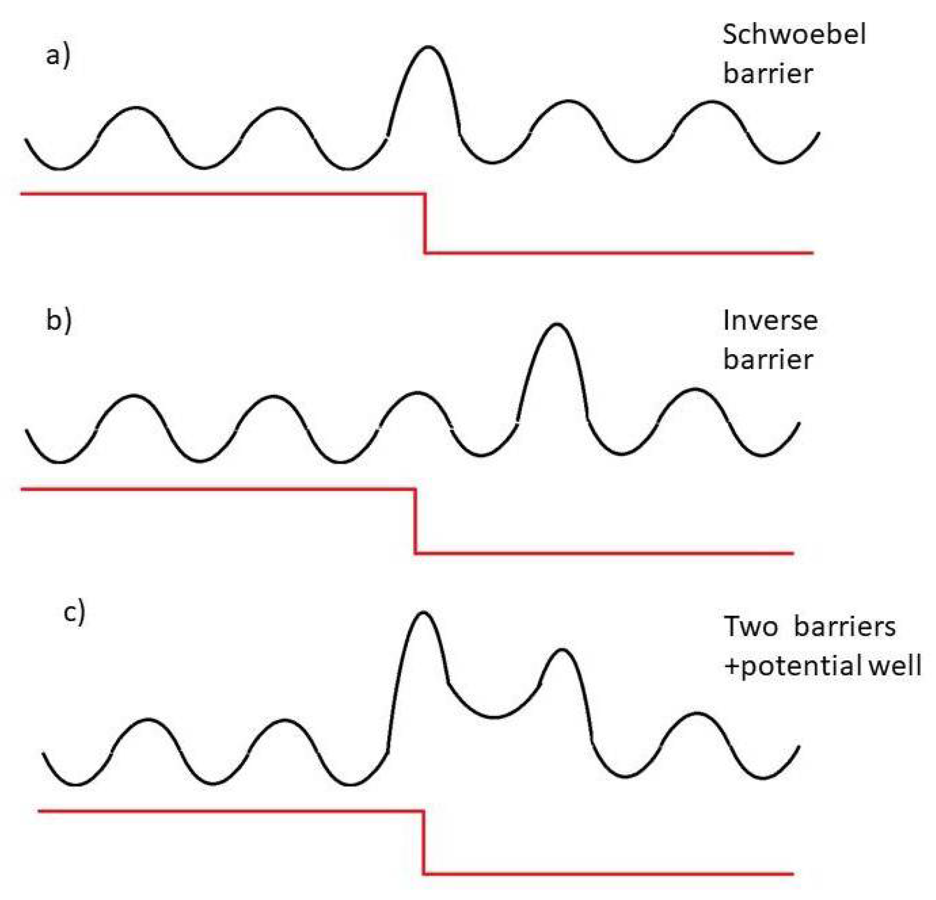
The source of the varying outputs of our simulations lies in the diffusion of adatoms. All particles diffuse along a given energy landscape that depends on the step position. Each particle diffuses independently, but double occupancy is forbidden. All jumps along terraces, except those in the immediate vicinity of the step, are performed with the same probability, which, after the equal choice of jump direction, is equal to 1. For jumps at the step different alternatives are studied. The classical choice is the direct Ehrlich-Schwoebel barrier (dES), located at the top of step (Figure 1a). Such a position for the barrier makes it difficult to jump across the step (down or up). We set a probability of such a jump PdES, which is 1 for no barrier and 0 for an infinite barrier. All other cases in between are studied. Similarly, we set inverse Schwoebel barrier PiES, which is located at the bottom of step (Figure 1b) and prevents particles from jumping towards step from below or back. We combined these two cases and added one more parameter pw, namely, such one that decides about the energy of particle that stays at the bottom of the step. The site at the bottom of the step is at a particular position, because adatoms that occupy this site interact with particles that build crystal steps, and their energy is changed by these interactions. An assumption of different potential energy at this particular point causes that the model is more realistic. Such a particle, if its energy is larger than in other positions, jumps more easily over a left-hand or right-hand barrier (Figure 1c), while if its energy is lower, its jump is more difficult. The parameter pw changes from 0 (which means that the particle is blocked at its position) to the lower value of PdES−1 or PiES−1 Particle jumps out of the site at the bottom of the step with a probability of pwPdES or pwPiES, and for the maximal value of pw, one of them is equal to 1. The parameter causing the jumping over barriers becomes asymmetric but fulfills the detailed balance condition. As we see, together with the CA rules for incorporation at steps, it allows particles to form various surface patterns, depending on the choice of all three parameters pw, PdES, and PiES. During the diffusion process, all adatoms try to perform nDS diffusional jumps, but only those that point at an unoccupied neighboring lattice site are performed.
Finally, the number of particles in the adatom cloud is randomly updated by the addition of particles so that at the end of each time step, the adatom concentration equals its initial value c0, thus setting equilibrium between the lattice gas and the ambience. The above procedure describes the sequence of a single time step and is repeated many times during each run of the simulation. Therefore, we measure the time in growth updates.
3. Pattern Formation
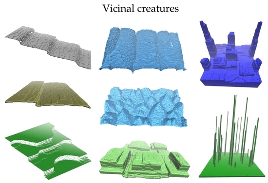
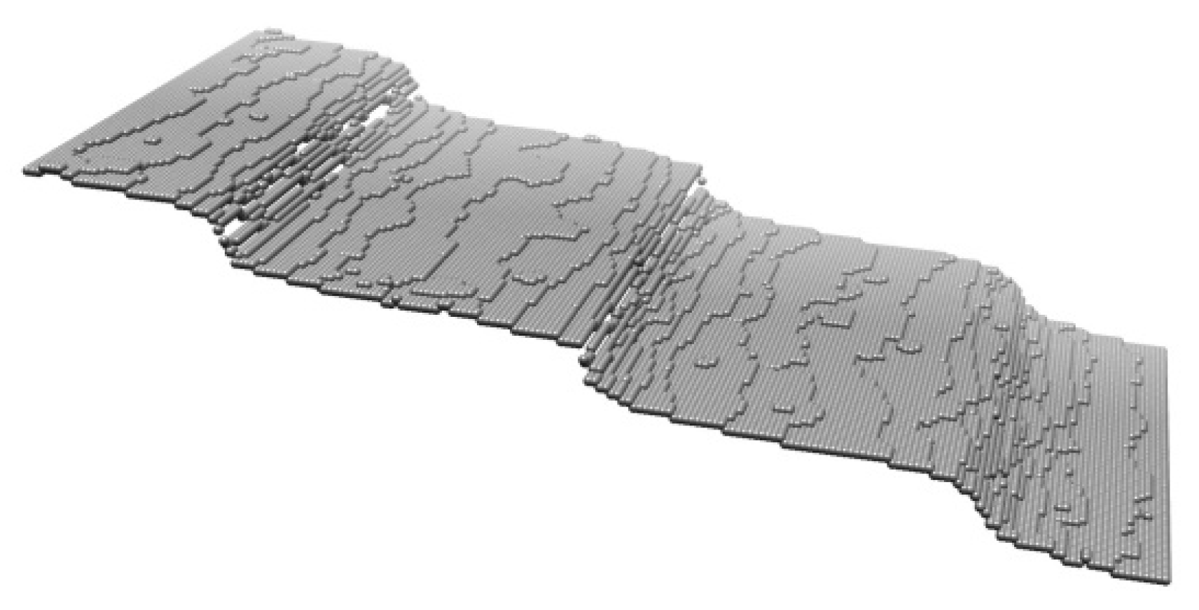
It is well known that the presence of dES located at the top of the step leads to step meandering in the process of crystal growth [14,27,28,34]. In Figure 2, we show the meandered surface obtained after 105 vicCA simulation time steps. We used the barrier of infinite height, given the probability of jumping across the steps PdES = 0. Each of the meandered steps are clearly seen in this plot. Together they form noticeable “fingers” in the direction vertical to the steps. Such fingers are quite often observed at the top of grown crystals.
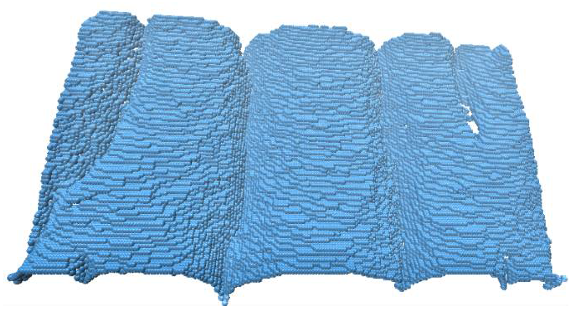
Another common situation is step bunch formation, and this can be attributed to the presence of iES (Refs. [14,30,31,35] and the references therein). We have applied such a barrier in our system, and the resulting bunches are shown in Figure 3. Again, we have used the infinite barrier, PiES = 0, and we show the system formed after 105 vicCA simulation time steps. Three bunches parallel to the initial step direction are well seen in the figure. It can be noted that due to the introduced possibility of particle nucleation, islands appear at wider terraces. We observed that at given conditions, islands are attached to the moving steps and do not initiate further 3D growth. The height of bunches increases with the longer time of the simulation.
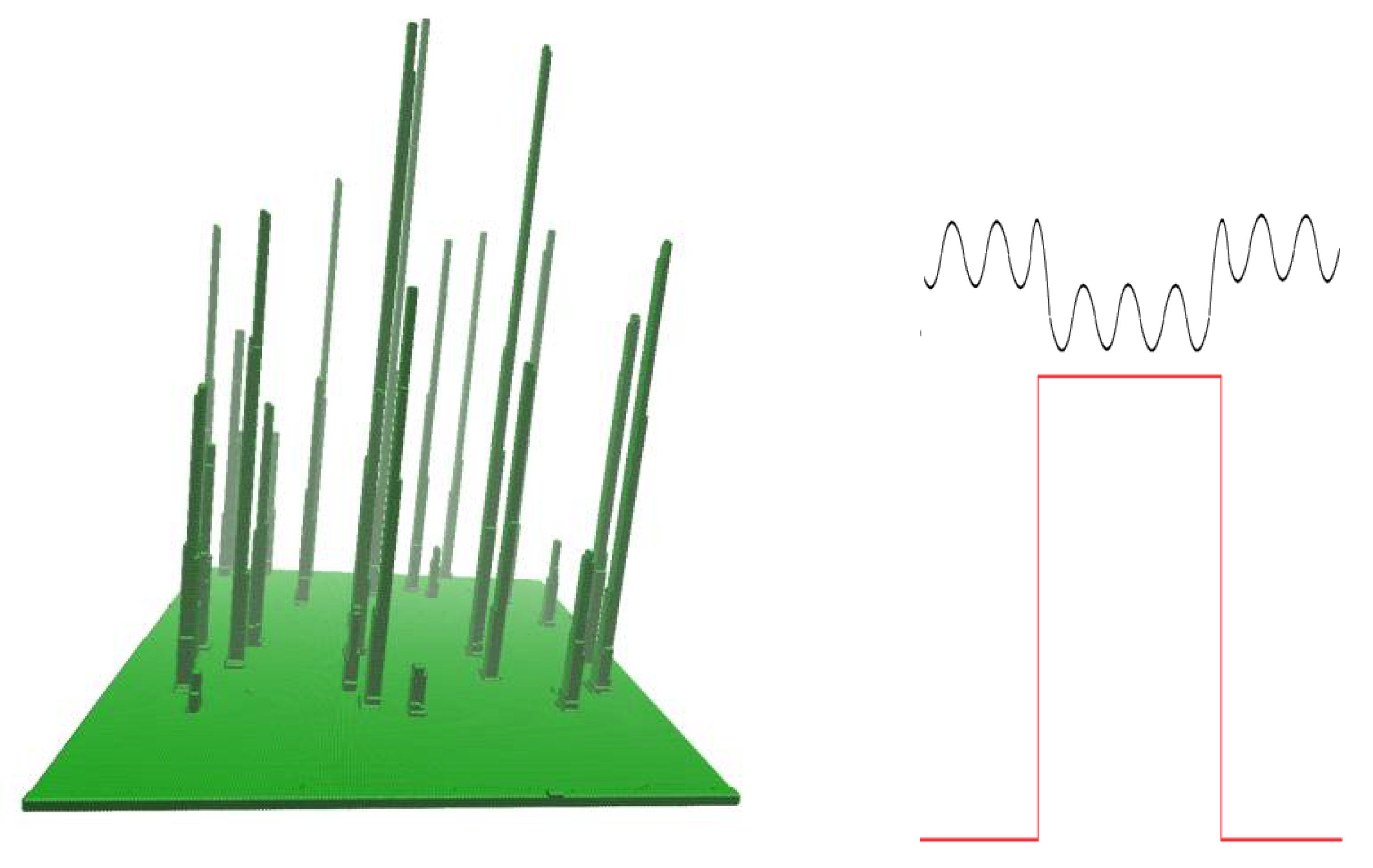
A third classical example that can be studied through the vicCA model is the growth of nanowire at the surface. The typical mode for nanowire formation is growing them under a cap, i.e., golden spot [1,2,3]. The role of such a spot is in changing energy potential under the cap, which means that sites under gold act like a local sink. We modeled such a system by assuming an asymmetric barrier at the top of the step. This barrier allows particles to jump up with probability 1 and to jump down from the top of the wire with probability PdES_asm = 0.1. In the example illustrated in Figure 4, resulting surface patterns with well-formed nanowires can be clearly seen. The potential landscape, in this case, is presented at the right side of the plot. Because of the asymmetry of dES, which is not compensated by the asymmetry of iES like in Figure 1c, this case leads to aggregation of particles on the top of islands. In this respect, this case is different from all other systems presented in the current work. We can see that such conditions result in creation of long, thin nanowires. The positions of nanowires are random because we do not initiate nanowire growth at given places on the surface. In addition, the energy potential in Figure 4 works only when nanowire is formed at the surface.
The three patterns shown above are examples of simple orderings that appear as a result of given shapes of the energy landscapes. Simple assumptions about the energy arrangement result in a well-defined surface pattern: dES causes meanders, iES causes bunches, and the existence of a lower potential on the top of the island leads to nanowire formation. Below we present the various surface patterns that are a consequence of the fact that adatom diffusion occurs at the potential linking the above cases. It turns out that we are able to reproduce several different patterns on the surface of a growing crystal. This is possible by changing the parameters of the step barriers dES, iES, and the energy level assigned to the position at the bottom of the step given by the probability pw. These patterns can be understood as a combination of the above-mentioned orderings or as a completely new system on the surface driven by a step potential.
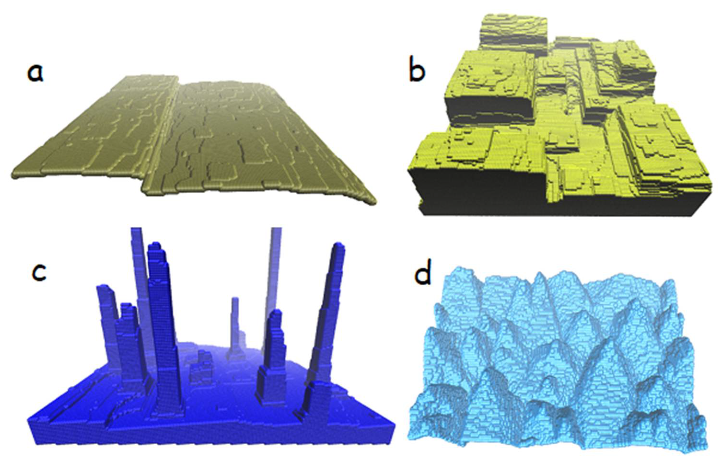
In Figure 5, we show four different three-dimensional surface formations that are found when the relative height of the barriers at steps is changed. Figure 5a shows bunches that are accompanied by antibunches. The crystal surface is the highest at the middle of the terrace, and it builds a bunch to the right, while to the left, a new bunch in the opposite direction is created. In the center, we see square or rectangular islands following the lattice symmetry. The shapes of the islands are caused by the cubic lattice we study here and CA rules of the attachment of particles to the crystal phase. These rules favor kink positions at the step, thus allowing the step to straighten up. Such a formation is found with parameters PiES = 0.2, PdES = 0.6. When decreasing PdES = 0.4, which means that the height of direct Schwoebel barrier dES increases and more particles are trapped at the top of the step, we get a very interesting new pattern, referred to as nanopillars or nanocolumns (Figure 5b). It consists of cubic formations, much wider than the initial inter-step distance l0. They have smooth, straight-up walls, and they grow very tall when the simulation continues. Finally, the gaps between these formations become narrow and very deep.
When PdES becomes smaller and is of the order of PiES, formations at the surface are closer to nanowires, as can be seen in Figure 5c, where the pattern obtained for PdES = 0.2 is shown. If these nanowires are compared to Figure 4, it can be seen that walls here are not so smooth, and nanowire diameter decreases with its height. Note, however, that these nanowires were created on setting the potential given in Figure 1c, not the one shown in the inset of Figure 4. Particles are not trapped at the top of the wire, as they are in the case of Figure 4. Nevertheless, without trapping, it was possible to build a structure with nanowires; this means no droplet to initiate and control nanowire growth is needed here. It should also be stressed here that we used low PdES, close to PiES, but not 0. It appears that when PdES is lowered to 0, we obtain another type of structure. In this case, the whole surface is covered by pyramids with similar shapes and sizes, as shown in Figure 5d. It is a very characteristic 3D formation, quite often generated at the surface of growing crystals. Such shapes change to classical meandered patterns shown in Figure 2 when the c0 is lower, and the particles attach to steps before they stick together and nucleate. In addition, this means that meanders are formed in the case of very slow growth, while 3D growth in the form of pyramids will be present for a faster crystal growth process. It is worth noting that all the above-mentioned orderings reflect the underlying symmetry of the lattice. Therefore, the islands have square or rectangular shapes, and the formations shown in Figure 5 are also squares. A hexagonal lattice as the base would convert these shapes to triangles or hexagons.
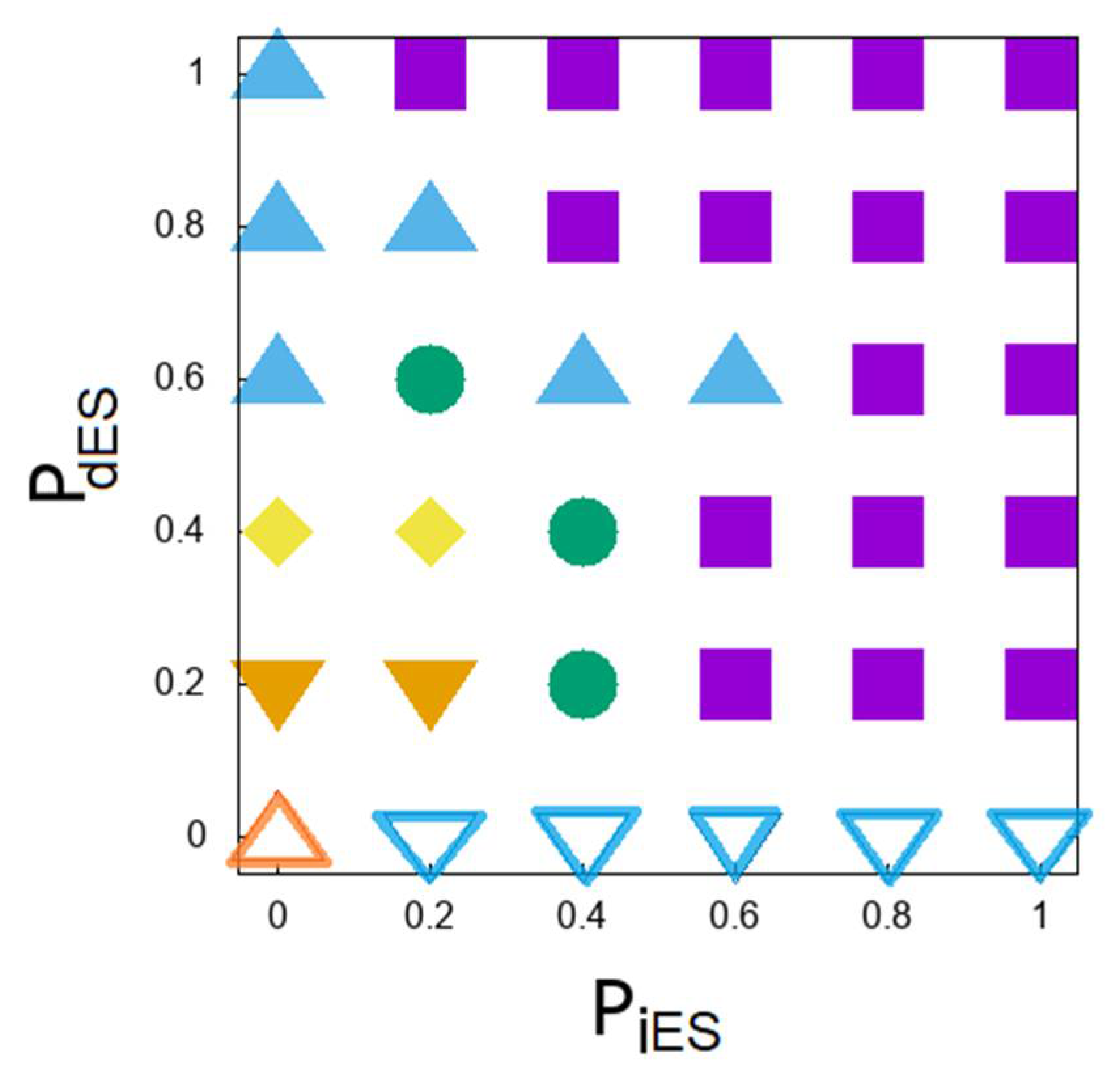
In order to examine the possible surface structures more systematically, we have scanned the system behavior as a function of PiES and PdES for one value of c0 = 0.02. PdES and PiES were changed by 0.2, and as a result, in Figure 6, we can see a map of possible orderings in this case. Let us note that a large part of this plot is covered by a regular structure, which means that steps move evenly, with small fluctuations, forming perfect crystal structures. Apart from the regular structure, we have all patterns mentioned above, except meanders that would replace pyramids in this diagram for lower c0, which refers to the lower particle flux, determining the crystal growth rate. The point (0,0) corresponding to infinite direct and inverse barriers is very specific. It concerns the situation where the particle cannot diffuse to the step, neither from the bottom nor from the top. The only possibility is to land exactly at the step, and only then the particle can attach to it. Such events happen but are very rare; hence, we see very slow growth of rather straight steps for these parameters.
4. Conclusions
We have demonstrated the main feasibility of using Cellular Automata to build rather realistic models of crystal growth and the instabilities that lead to pattern formation. Moreover, we have demonstrated the power of such a model for (“in silico”) bottom-up synthesis of various nanostructures. The combination of dES, iES, and one additional nucleation rule for island formation made it possible to control and change the pattern formation from bunches, antibunches, nanocolumns, nanowires, and finally meanders or pyramids. There is also a wide range of parameters that lead to stable crystal growth through even step motion. The model is simple, and large systems in long runs can be simulated, which allows for systematic, quantitative studies on the selected effect. With further refinement, this model could be used to build a completely new platform for studying nanoscale phenomena.
Author Contributions
M.Z.-K., H.P. and V.T. performed numerical calculations; M.Z.-K., H.P. and V.T. analyzed the data; M.Z.-K., H.P. and V.T. wrote the paper. All the authors contributed equally. All authors have read and agreed to the published version of the manuscript.
Funding
This research received no external funding.
Acknowledgments
Part of the calculations was done on HPC facility Nestum (BG161PO003-1.2.05). This article is based upon work from COST Action 18234, supported by COST (European Cooperation in Science and Technology).
Conflicts of Interest
The authors declare no conflict of interest.
Appendix A. Table of Cellular Automaton Rules
The realization of CA step of the vicCA model is based on 2 × 81 CA rules. We enumerate them in a table below. The rule is a function of five discrete parameters. The value of this function is 0 or 1. Value 0 means that no action is performed, and value 1 means that the adatom at the given site is incorporated in a crystal phase. The first parameter of the function corresponds to an adatom, and it is equal to 1 when an adatom is present at a given site and 0 if the site is empty. Note that this parameter has two different values, which duplicates sets of possible CA rules. When it is equal to 0, there is only one situation, the filling voids case, in which the rule gives the value 1. All other situations have an outcome zero. The next four parameters correspond to the states of neighboring sites in a sequence right, down, left, and up. Each of the neighbors can be in one of the three states (0,1,2): state 2, which means that up step is present there (or we have a crystal atom in this cell); state 1, which means that we have an adatom there; and state 0, which means none of these cases.
| Crystal seed Rule(1,1,1,1,0) = 1 Rule(1,1,0,1,1) = 1 Rule(1,1,1,1,1) = 1 Adsorption at step Rule(1,0,0,1,2) = 1 Rule(1,0,0,2,1) = 1 Rule(1,0,1,2,0) = 1 Rule(1,1,2,0,0) = 1 Rule(1,2,1,0,0) = 1 Rule(1,2,0,0,1) = 1 Rule(1,0,1,1,2) = 1 Rule(1,0,1,2,1) = 1 Rule(1,0,2,1,1) = 1 Rule(1,1,0,1,2) = 1 Rule(1,1,0,2,1) = 1 Rule(1,1,1,0,2) = 1 Rule(1,1,1,2,0) = 1 Rule(1,1,2,0,1) = 1 Rule(1,1,2,1,0) = 1 Rule(1,2,0,1,1) = 1 Rule(1,2,1,0,1) = 1 Rule(1,2,1,1,0) = 1 Rule(1,1,1,1,2) = 1 Rule(1,1,1,2,1) = 1 Rule(1,1,2,1,1) = 1 Rule(1,2,1,1,1) = 1 Rule(1,0,2,1,0) = 1 Rule(1,1,0,0,2) = 1 | Adsorption at kink Rule(1,0,0,2,2) = 1 Rule(1,0,2,2,0) = 1 Rule(1,2,0,0,2) = 1 Rule(1,2,2,0,0) = 1 Rule(1,0,1,2,2) = 1 Rule(1,0,2,1,2) = 1 Rule(1,0,2,2,1) = 1 Rule(1,1,0,2,2) = 1 Rule(1,1,2,0,2) = 1 Rule(1,1,2,2,0) = 1 Rule(1,2,0,1,2) = 1 Rule(1,2,0,2,1) = 1 Rule(1,2,1,0,2) = 1 Rule(1,2,1,2,0) = 1 Rule(1,2,2,0,1) = 1 Rule(1,2,2,1,0) = 1 Rule(1,0,2,2,2) = 1 Rule(1,2,0,2,2) = 1 Rule(1,2,2,0,2) = 1 Rule(1,2,2,2,0) = 1 Rule(1,1,1,2,2) = 1 Rule(1,1,2,1,2) = 1 Rule(1,1,2,2,1) = 1 Rule(1,2,1,1,2) = 1 Rule(1,2,1,2,1) = 1 Rule(1,2,2,1,1) = 1 Rule(1,1,2,2,2) = 1 Rule(1,2,1,2,2) = 1 Rule(1,2,2,1,2) = 1 Rule(1,2,2,2,1) = 1 Rule(1,2,2,2,2) = 1 | Filling voids Rule(0,1,1,1,1) = 1 No Adsorption Rule(1,0,0,0,0) = 0 Rule(1,0,0,0,1) = 0 Rule(1,0,0,1,0) = 0 Rule(1,0,1,0,0) = 0 Rule(1,1,0,0,0) = 0 Rule(1,0,0,1,1) = 0 Rule(1,0,1,0,1) = 0 Rule(1,0,1,1,0) = 0 Rule(1,0,0,1,1) = 0 Rule(1,1,0,1,0) = 0 Rule(1,1,0,0,1) = 0 Rule(1,1,1,0,1) = 0 Rule(1,0,1,1,1) = 0 Rule(1,0,0,0,2) = 0 Rule(1,0,0,2,0) = 0 Rule(1,0,2,0,0) = 0 Rule(1,2,0,0,0) = 0 Rule(1,0,1,0,2) = 0 Rule(1,0,2,0,1) = 0 Rule(1,1,0,2,0) = 0 Rule(1,2,0,1,0) = 0 Rule(1,0,2,0,2) = 0 Rule(1,2,0,2,0) = 0 Rule(0,*,*,*,*) = 0 |
References
- Oreg, Y.; Refael, G.; von Oppen, F. Helical Liquids and Majorana Bound States in Quantum Wires. Phys. Rev. Lett. 2010, 105, 177002. [Google Scholar] [CrossRef] [Green Version]
- Lutchyn, R.M.; Sau, J.D.; Das Sarma, S. Majorana Fermions and a Topological Phase Transition in Semiconductor-Superconductor Heterostructures. Phys. Rev. Lett. 2010, 105, 077001. [Google Scholar] [CrossRef] [Green Version]
- Mourik, V.; Zuo, K.; Frolov, S.M.; Plissard, S.R.; Bakkers, E.P.a.M.; Kouwenhoven, L.P. Signatures of Majorana Fermions in Hybrid Superconductor-Semiconductor Nanowire Devices. Science 2012, 336, 1003–1007. [Google Scholar] [CrossRef] [Green Version]
- Grünberg, P.; Schreiber, R.; Pang, Y.; Brodsky, M.B.; Sowers, H. Layered Magnetic Structures: Evidence for Antiferromagnetic Coupling of Fe Layers across Cr Interlayers. Phys. Rev. Lett. 1986, 57, 2442. [Google Scholar] [CrossRef] [PubMed]
- Baibich, M.N.; Broto, J.M.; Fert, A.; Nguyen, V.D.F.; Petroff, F.; Etienne, P.; Creuzet, G.; Friederich, A.; Chazelas, J. Giant Magnetoresistance of (001)Fe/(001)Cr Magnetic Superlattices. Phys. Rev. Lett. 1988, 61, 2472. [Google Scholar] [CrossRef] [PubMed] [Green Version]
- Fermon, C.; Pannetier-Lecoeur, M. Noise in GMR and TMR Sensors. In Giant Magnetoresistance (GMR) Sensors. Smart Sensors, Measurement and Instrumentation; Reig, C., Cardoso, S., Mukhopadhyay, S.C., Eds.; Springer: Berlin/Heidelberg, Germany, 2013; Volume 6, pp. 47–70. [Google Scholar]
- Zheludev, N. The life and times of the LED—A 100-year history. Nat. Photonics 2007, 1, 189–192. [Google Scholar] [CrossRef]
- Isobe, Y.; Iida, D.; Sakakibara, T.; Iwaya, M.; Takeuchi, T.; Kamiyama, S.; Akasaki, I.; Amano, H.; Imade, M.; Kitaoka, Y.; et al. Growth of AlGaN/GaN heterostructure on vicinal m-plane free-standing GaN substrates prepared by the Na flux method. Phys. Status Solidi (A) Appl. Mater. Sci. 2011, 208, 1191–1194. [Google Scholar] [CrossRef]
- Amano, H.; Sawaki, N.; Akasaki, I. Metalorganic vapor phase epitaxial growth of a high quality GaN film using an AlN buffer layer. Appl. Phys. Lett. 1986, 48, 353. [Google Scholar] [CrossRef] [Green Version]
- Yang, J.J.; Pickett, M.D.; Li, X.; Ohlberg, D.A.A.; Stewart, D.R.; Williams, R.S. Memristive switching mechanism for metal/oxide/metal nanodevices. Nat. Nanotechnol. 2008, 3, 429–433. [Google Scholar] [CrossRef]
- Yang, J.J.; Strukov, D.B.; Stewart, D.R. Memristive Devices for Computing. Nat. Nanotechnol. 2013, 8, 13–24. [Google Scholar] [CrossRef]
- Ehrlich, G.; Hudda, F.G. Atomic view of surface self-diffusion—Tungsten on tungsten. J. Chem. Phys. 1966, 44, 1039. [Google Scholar] [CrossRef]
- Schwoebel, R.L.; Shipsey, E.J. Step motion on crystal surfaces. J. Appl. Phys. 1966, 37, 3682. [Google Scholar] [CrossRef]
- Misbah, C.; Pierre-Louis, O.; Saito, Y. Crystal surfaces in and out of equilibrium: A modern view. Rev. Mod. Phys. 2010, 82, 981. [Google Scholar] [CrossRef]
- Saúl, A.; Métois, J.-J.; Ranguis, A. Experimental evidence for an Ehrlich-Schwoebel effect on Si(111). Phys. Rev. B 2001, 65, 075409. [Google Scholar] [CrossRef]
- Rogilo, D.I.; Fedina, L.I.; Kosolobov, S.S.; Ranguelov, B.S.; Latyshev, A.V. Critical Terrace Width for Two-Dimensional Nucleation during Si Growth on Si(111)-(7 × 7) Surface. Phys. Rev. Lett. 2013, 111, 036105. [Google Scholar] [CrossRef]
- De Theije, F.K.; Schermer, J.J.; Van Enckevort, W.J.P. Effects of nitrogen impurities on the CVD growth of diamond: Step bunching in theory and experiment. Diam. Relat. Mater. 2000, 9, 1439–1449. [Google Scholar] [CrossRef]
- Xie, M.H.; Cheung, S.H.; Zheng, L.X.; Ng, Y.F.; Wu, H.; Ohtani, N.; Tong, S.Y. Step bunching of vicinal GaN(0001) surfaces during molecular beam epitaxy. Phys. Rev. B Condens. Matter Mater. Phys. 2000, 61, 9983–9985. [Google Scholar] [CrossRef] [Green Version]
- Zheng, H.; Xie, M.H.; Wu, H.S.; Xue, Q.K. Kinetic energy barriers on the GaN (0001) surface: A nucleation study by scanning tunneling microscopy. Phys. Rev. B 2008, 77, 045303. [Google Scholar] [CrossRef]
- Gianfrancesco, A.G.; Tselev, A.; Baddorf, A.P.; Kalinin, S.V.; Vasudevan, R.K. The Ehrlich–Schwoebel barrier on an oxidesurface: A combined Monte-Carlo and in situ scanning tunneling microscopy approach. Nanotechnology 2015, 26, 455705. [Google Scholar] [CrossRef]
- Sarma, D.S.; Punyindu, P.; Toroczkai, Z. Non-universal mound formation in non-equilibrium surface growth Z. Surf. Sci. 2000, 457, L369–L375. [Google Scholar] [CrossRef] [Green Version]
- Leal, F.F.; Ferreira, S.C.; Ferreira, S.O. Modelling of epitaxial film growth with an Ehrlich–Schwoebel barrier dependent on the step height. J. Phys. Condens. Matter. 2011, 23, 292201. [Google Scholar] [CrossRef] [Green Version]
- Palczynski, K.; Herrmann, P.; Heimel, G.; Dzubiella, J. Characterization of step-edge barrier crossing of para-sexiphenyl on the ZnO (101 [combining macron] 0) surface. J. Phys. Chem. Chem. Phys. 2016, 18, 25329. [Google Scholar] [CrossRef]
- Xiang, S.K.; Huang, H. Ab initio determination of Ehrlich–Schwoebel barriers on Cu {111}. Appl. Phys. Lett. 2008, 92, 101923. [Google Scholar] [CrossRef]
- Hao, J.; Zhang, L. Strongly reduced Ehrlich–Schwoebel barriers at the Cu (111) stepped surface with In and Pb surfactants. Surf. Sci. 2018, 667, 13–16. [Google Scholar] [CrossRef]
- Xie, M.H.; Leung, S.Y.; Tong, S.Y. What causes step bunching-negative Ehrlich-Schwoebel barrier versus positive incorporation barrier. Surf. Sci. 2002, 515, L459–L463. [Google Scholar] [CrossRef]
- Krzyżewski, F.; Załuska–Kotur, M.A. Coexistence of bunching and meandering instability in simulated growth of 4H-SiC (0001) surface. J. Appl. Phys. 2014, 115, 213517. [Google Scholar] [CrossRef] [Green Version]
- Krzyżewski, F.; Załuska-Kotur, M.A. Stability diagrams for the surface patterns of GaN (0001¯) as a function of Schwoebel barrier height. J. Cryst. Growth 2017, 457, 80–84. [Google Scholar] [CrossRef]
- Krasteva, A.; Popova, H.; Krzyżewski, F.; Załuska-Kotur, M.; Tonchev, V. Unstable vicinal crystal growth from cellular automata. AIP Conf. Proc. 2016, 1722, 220014. [Google Scholar]
- Krzyżewski, F.; Załuska-Kotur, M.A.; Krasteva, A.; Popova, H.; Tonchev, V. Step bunching and macrostep formation in 1D atomistic scale model of unstable vicinal crystal growth. J. Cryst. Growth 2017, 474, 135–139. [Google Scholar] [CrossRef] [Green Version]
- Krzyżewski, F.; Załuska-Kotur, M.A.; Krasteva, A.; Popova, H.; Tonchev, V. Scaling and Dynamic Stability of Model Vicinal Surfaces. Cryst. Growth Des. 2019, 19, 821–831. [Google Scholar] [CrossRef]
- Toktarbaiuly, O.; Usov, V.O.; Coileáin, C.; Siewierska, K.; Krasnikov, S.; Norton, E.; Bozhko, S.I.; Semenov, V.N.; Chaika, A.N.; Murphy, B.E.; et al. Step bunching with both directions of the current: Vicinal W(110) surfaces versus atomistic-scale model. Phys. Rev. B Condens. Matter Mater. Phys. 2018, 97, 035436. [Google Scholar] [CrossRef] [Green Version]
- Popova, H.; Krzyżewski, F.; Załuska-Kotur, M.A.; Tonchev, V. Quantifying the Effect of Step–Step Exclusion on Dynamically Unstable Vicinal Surfaces: Step Bunching without Macrostep Formation. Cryst. Growth Des. 2020, 20, 7246–7259. [Google Scholar] [CrossRef]
- Turski, H.; Krzyżewski, F.; Feduniewicz-Żmuda, A.; Wolny, P.; Siekacz, M.; Muziol, G.; Cheze, C. Nowakowski-Szukudlarek Krzesimir, Xing Huili Grace, Jena Debdeep, Załuska-Kotur Magdalena, Skierbiszewski Czesław, Unusual step meandering due to Ehrlich-Schwoebel barrier in GaN epitaxy on the N-polar Surface. Appl. Surf. Sci. 2019, 484, 771–780. [Google Scholar] [CrossRef] [Green Version]
- Sato, M.; Uwaha, M. Growth law of step bunches induced by the Ehrlich-Schwoebel effect in growth. Surf. Sci. 2001, 493, 494–498. [Google Scholar] [CrossRef]
Figure 1.
Energy landscape for diffusing particles. (a) Direct Ehrlich–Schwoebel (dES) barrier at the top of the step, with jump probability given by PdES. (b) Inverse Ehrlich–Schwoebel (iES) barrier below the step with jump probability given by PiES. (c) PdES, PiES and the changed depth of the potential well below. The jump rate out of the well is described by parameter pw.

Figure 2.
Meanders, c0 = 0.01, PiES = 1, PdES = 0, pw = 1, l0 = 5, nDS = 10. System size 200 × 200.

Figure 3.
Bunches, c0 = 0.02, PiES = 0, PdES = 1, pw = 1, l0 = 10, nDS = 10. System size 300 × 100.

Figure 4.
Nanowires, c0 = 0.02, PiES = 0, PdES_asm = 0.1, pw = 1, nDS = 10, l0 = 100. System size 200 × 200. Inset: potential that realizes given pattern.
Figure 4.
Nanowires, c0 = 0.02, PiES = 0, PdES_asm = 0.1, pw = 1, nDS = 10, l0 = 100. System size 200 × 200. Inset: potential that realizes given pattern.

Figure 5.
(a) Antibunches, c0 = 0.02, PiES = 0.2, PdES = 0.6, pw = 1.66, l0 = 10, nDS = 10, time steps 3 × 10⁶. (b) Nanopillars, c0 = 0.02, PiES = 0.2, PdES = 0.4, pw = 2.5, l0 = 10, nDS = 10, time steps 2 × 10⁵. (c) Nanowires, c0 = 0.02, PiES = 0.1, PdES = 0.2, pw = 5, l0 = 10, nDS = 10, time steps 3 × 10⁵. (d) Pyramids, c0 = 0.02, PiES = 1.0, PdES = 0.0, pw = 1.0, l0 = 5, nDS = 10, time steps 4 × 10⁵.

Figure 6.
Diagram of pattern formation. Different symbols correspond to different patterns: ![Crystals 11 01135 i001]() describes regular step ordering,
describes regular step ordering, ![Crystals 11 01135 i002]() means bunches,
means bunches, ![Crystals 11 01135 i003]() bunches with antibunches,
bunches with antibunches, ![Crystals 11 01135 i004]() describe nanopillars,
describe nanopillars, ![Crystals 11 01135 i005]() nanowires,
nanowires, ![Crystals 11 01135 i006]() pyramids, and
pyramids, and ![Crystals 11 01135 i007]() is specific (0, 0) point.
is specific (0, 0) point.
 describes regular step ordering,
  means bunches,
  bunches with antibunches,
  describe nanopillars,
  nanowires,
  pyramids, and
  is specific (0, 0) point.
Figure 6.
Diagram of pattern formation. Different symbols correspond to different patterns: ![Crystals 11 01135 i001]() describes regular step ordering,
describes regular step ordering, ![Crystals 11 01135 i002]() means bunches,
means bunches, ![Crystals 11 01135 i003]() bunches with antibunches,
bunches with antibunches, ![Crystals 11 01135 i004]() describe nanopillars,
describe nanopillars, ![Crystals 11 01135 i005]() nanowires,
nanowires, ![Crystals 11 01135 i006]() pyramids, and
pyramids, and ![Crystals 11 01135 i007]() is specific (0, 0) point.
is specific (0, 0) point.
describes regular step ordering, means bunches, bunches with antibunches, describe nanopillars, nanowires, pyramids, and is specific (0, 0) point.
Publisher’s Note: MDPI stays neutral with regard to jurisdictional claims in published maps and institutional affiliations. |
© 2021 by the authors. Licensee MDPI, Basel, Switzerland. This article is an open access article distributed under the terms and conditions of the Creative Commons Attribution (CC BY) license (https://creativecommons.org/licenses/by/4.0/).
Share and Cite
MDPI and ACS Style
Załuska-Kotur, M.; Popova, H.; Tonchev, V. Step Bunches, Nanowires and Other Vicinal “Creatures”—Ehrlich–Schwoebel Effect by Cellular Automata. Crystals 2021, 11, 1135. https://0-doi-org.brum.beds.ac.uk/10.3390/cryst11091135
AMA Style
Załuska-Kotur M, Popova H, Tonchev V. Step Bunches, Nanowires and Other Vicinal “Creatures”—Ehrlich–Schwoebel Effect by Cellular Automata. Crystals. 2021; 11(9):1135. https://0-doi-org.brum.beds.ac.uk/10.3390/cryst11091135
Chicago/Turabian StyleZałuska-Kotur, Magdalena, Hristina Popova, and Vesselin Tonchev. 2021. "Step Bunches, Nanowires and Other Vicinal “Creatures”—Ehrlich–Schwoebel Effect by Cellular Automata" Crystals 11, no. 9: 1135. https://0-doi-org.brum.beds.ac.uk/10.3390/cryst11091135
Note that from the first issue of 2016, this journal uses article numbers instead of page numbers. See further details here.