Article

Numerical Simulation of β-Ga2O3 Single Crystal Growth by Czochralski Method with an Insulation Lid

1
State Key Laboratory of Silicon Materials, School of Materials Science and Engineering, Zhejiang University, Hangzhou 310027, China
2
Zhejiang Provincial Key Laboratory of Power Semiconductor Materials and Devices, ZJU-Hangzhou Global Scientific and Technological Innovation Center, Hangzhou 311200, China
*
Authors to whom correspondence should be addressed.
Submission received: 4 November 2022 / Revised: 18 November 2022 / Accepted: 21 November 2022 / Published: 25 November 2022
(This article belongs to the Special Issue Heat and Mass Transfer Modeling in Crystal Growth)

Abstract

:
The effect of an insulation lid on the growth of 4-inch β-Ga2O3 single crystals by the Czochralski method is analyzed by numerical simulation. The insulation lid mainly hinders upward radiant heat transfer from the melt and crucible and increases the axial temperature gradient in the crystal. Such benefits make the melt/crystal interface convex, which is conducive to suppressing spiral growth and growing large crystals with high quality. Materials with low thermal conductivity λ and low emissivity ε are the optimal choices for making an insulation lid. The inner hole has a great influence on the isolation of radiant heat, and it is determined that the maximum size of the inner diameter D i n should not be larger than 130 mm. Thermal stress analysis results indicated that the insulation lid will cause a better stress distribution, illustrating the effect of the insulation lid on the quality of a cylindrical crystal.

1. Introduction

Gallium oxide (β-Ga2O3) is an ultra-wide bandgap (UWBG) semiconductor that has attracted much attention in recent years due to its ultra-wide bandgap width and high breakdown electric field strength, as well as its large optical transmission range and high-quality factor of Baliga’s figure of merit (BFOM) [1,2]. Because of its outstanding properties, it has obvious advantages in applications for high-voltage power devices such as metal oxide semiconductor field effect transistors (MOSFETs), Schottky barrier diodes (SBD), and deep ultraviolet (DUV) photodetectors [2,3,4]. There have been many basic studies on β-Ga2O3, such as those about defects and impurities, leading to β-Ga2O3 being successfully applied as a material for power electronics and optoelectronics of the DUV range [5]. β-Ga2O3 single crystals with a large diameter and high quality are required by the rapid expansion of market requirements [6]. Therefore, melting growth methods that can obtain high-quality β-Ga2O3 crystals at low cost have become the preferred choice and research focus, such as the Czochralski (CZ) method [7,8,9,10,11,12], edge-defined film-fed growth (EFG) method [13,14,15,16], Bridgman method [17,18], and optical floating-zone method [19,20]. Among them, the CZ method enables the growth of columnar β-Ga2O3 single crystals with a large diameter, which is conducive to the preparation of wafers with different orientations. However, Galazka et al. [9] reported that spiral growth usually occurs in the growth of β-Ga2O3 single crystals by the CZ method due to the free carrier absorption of β-Ga2O3 crystals in the near-infrared (NIR) wavelength range. For the growth of crystals with a large diameter, i.e., 2 inches or larger, the solutions they propose are lowering the free electron concentration in the crystal or inducing an insulating state when doped with Mg, which provide a high rate of heat removal from the growth interface [8]. However, for crystals with a high free electron concentration, there is not yet an effective approach. Spiral growth is mainly caused by the concave interface [1,21]; thus, modifying the interface shape is conducive to suppressing spiral growth.
Numerical simulation is an effective tool to study heat transfer in crystal growth and design a thermal field subsequently, which is conductive to solving the problem mentioned above. Researchers have conducted many numerical works to build models and analyze the heat transfer in CZ growth, leading to the optimization of design of the thermal field, such as the optimizations of the crucible position [22], heat shield design [23,24], radio frequency (RF) coils’ position [25,26], furnace enclosure shape [27], and so on. Tang et al. [28] mainly simulated the flow field of a Ga2O3 melt and analyzed the difficulties of growing large-size bulk β-Ga2O3 single crystals via CZ growth. Furthermore, the quality of crystals is greatly affected by stress, which makes the study of stress essential. Miller et al. [29] provided a numerical model of the CZ growth of β-Ga2O3 single crystals and analyzed the three-dimensional (3D) simulation of thermal stress. In the present work, we introduce a CZ growth system with an insulation lid, which is a feasible idea for the growth of high-quality, 4-inch β-Ga2O3 single crystals by the CZ method. The insulation lid can effectively increase the temperature gradient in the crystal, which is conducive to modifying the interface shape and suppressing spiral growth. It is effective even for crystals with high free electron concentrations. The effect of the insulation lid is first analyzed by temperature distributions and the corresponding melt/crystal interface shapes. The heat transfer of the insulation lid is also analyzed to clarify its concrete effect on different heat transfer modes. The material parameters and the effect of the insulation lid’s inner hole are also discussed to determine the material selection and the size of the inner diameter. At last, the Von Mises stress distributions in crystals grown without or with an insulation lid are compared to illustrate its effect on the quality of cylindrical crystals.

2. Numerical Models

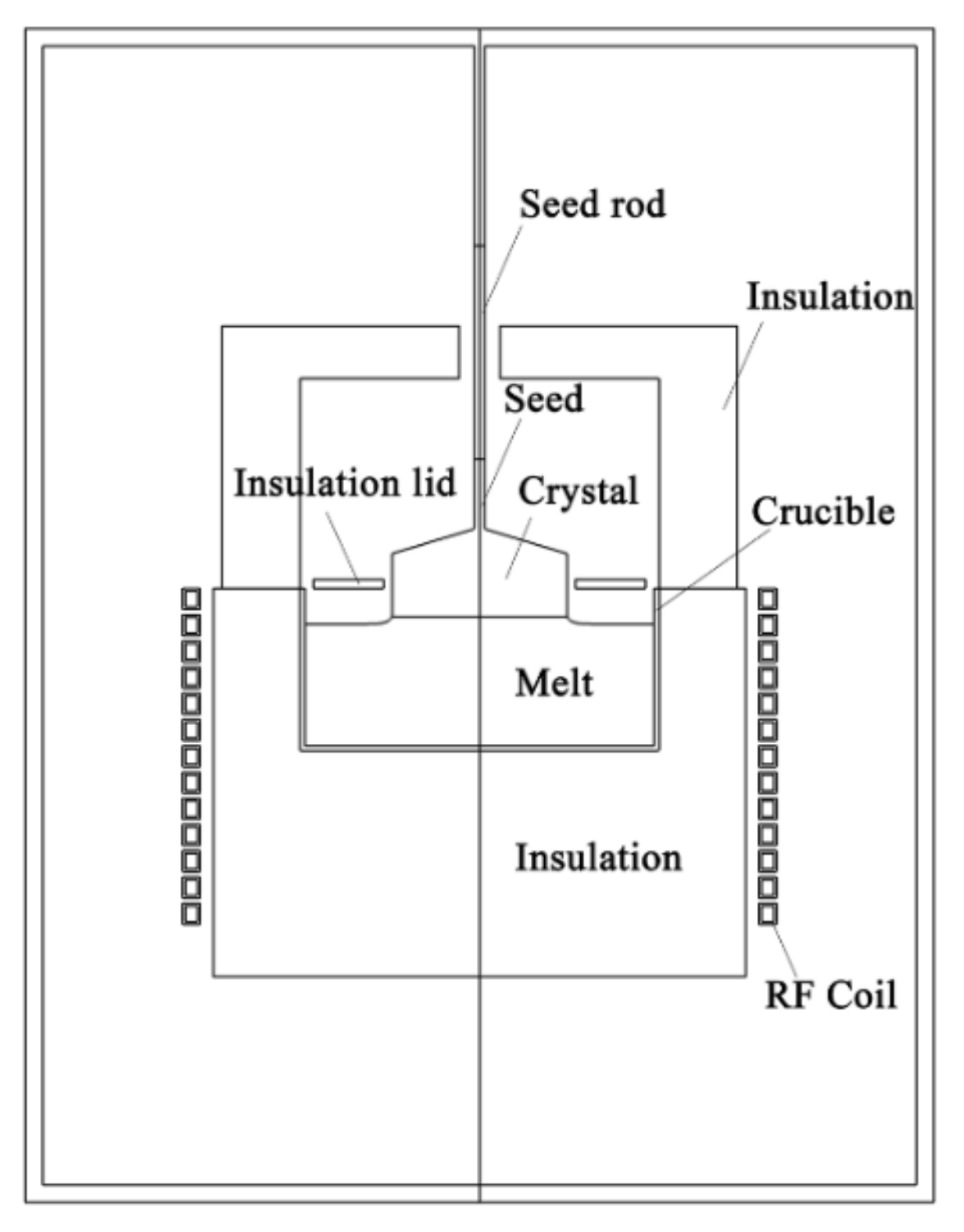
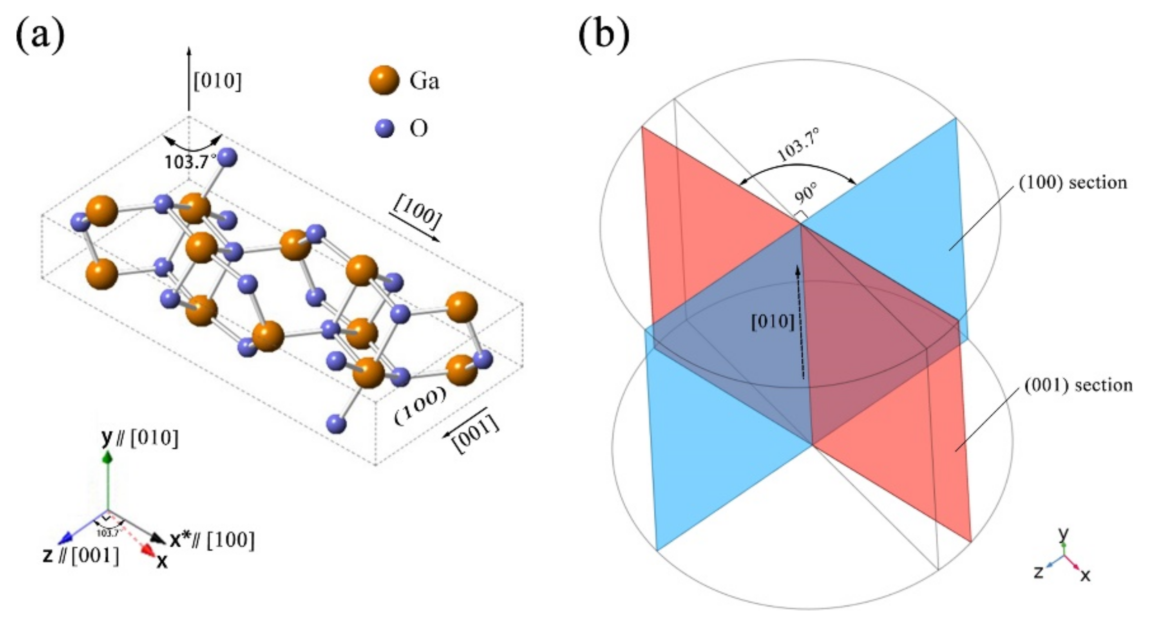
2.1. Geometric Model and Material Properties

Figure 1 shows the CZ system for the growth of a 4-inch β-Ga2O3 single crystal, consisting of an insulation lid, a crucible, a seed rod, a RF coil, and insulation components. The insulation lid is circular in structure, with an inner hole allowing the seed and crystal to pass through. It is located above the free surface of the melt and can be placed at the crucible mouth or suspended by an extra lifting device. The crucible is made of iridium, and its inside diameter is set as 200 mm to satisfy a crystal/crucible ratio approach of 0.5 [10] and a crucible aspect ratio of 0.45 (i.e., the crucible height is 0.45 times the crucible diameter). The seed rod is made of iridium and provides a pulling rate of 1.5 mm/h and a rotation rate of 2 RPM. The pulling direction is parallel to the [010] crystal orientation. The insulation components surrounding the crucible provide a suitable environment for crystal growth, and the viewing window on the side is ignored in the present simulation work. In the absence of specific instructions, the atmosphere in the growth furnace is set to be composed of Ar gas. The material properties utilized in the present simulation are summarized in Table 1.

2.2. Mathematical Models

The stable growth stage of a β-Ga2O3 single crystal is modeled in present work. A two-dimensional (2D) axisymmetric model was established to analyze the global heat transfer problem, taking into account the melt convection coupled to the gas flow. The following assumptions are made in the global model:
(1) The CZ system is quasi-steady-state due to relatively low crystallization rates. (2) The melt is composed of incompressible Newtonian fluids which satisfy the Boussinesq approximation. (3) The gas is incompressible, and the gas flow satisfies the low Mach number approximation and the ideal gas law. (4) Radiative heat exchange between any solid surfaces through a non-participating fluid is accounted for on the assumption of gray-diffusive surface radiation. (5) Because of the free carrier absorption of the β-Ga2O3 crystal in the near-infrared (NIR) wavelength range [9], in the present work, the crystal domain is assumed to be opaque to reach a limit state of NIR absorption. Based on the above assumptions, the governing equations are as follows [32,33]:
In solid domains (with induction heating):
· λ s T + Q = 0
In solid domains (without induction heating):
· λ s T = 0
In the melt domain:
· u = 0
ρ u · u = ρ + · τ ^ + ρ β T T 0 g
ρ u · T = · μ P r + μ t P r t T
In the gas domain:
· ρ g u g = 0
ρ g u g · u g = p g + · τ ^ + ρ g ρ 0 g
· ρ g u g C pg T = · λ g T
Radiation transfer on the surface:
s i n θ r c o s φ r I rad r s i n θ I rad φ + c o s θ I rad z + β rad I rad = F rad
I rad = 1 ε q rad inc π + ε σ T 4
At the melt/crystal interface:
V crys = 1 ρ crys · H λ crys T crys n λ melt T melt n
where λ s is thermal conductivity in solid domains, T is temperature, Q is the heat source, u is melt velocity, ρ is the density, τ ^ is the stress tensor, β is the thermal expansion coefficient, T 0 is the melt reference temperature, g is the gravity vector, μ is the melt dynamic viscosity, μ t is the turbulent effective viscosity, P r is the Prandtl number, P r t is the turbulent Prandtl number taken to be 0.9, ρ g is the density of gas, u g is melt velocity, p g is gas pressure, ρ 0 is the reference density, C pg is specific heat, λ g is heat conductivity of gas, I rad = I rad r , Ω is the radiation intensity at point r = x ,   y ,   z = r c o s φ r ,   r s i n φ r ,   z in the direction Ω = x ,   y ,   z = s i n θ c o s φ Ω , s i n θ s i n φ Ω ,   c o s θ , φ = φ Ω φ r , β rad is the extinction coefficient, F rad is the scattering integral, ε is the thermal emissivity of the opaque media, q rad inc is the radiative heat flux that is incident upon the surface, σ is the Stefan–Boltzmann constant, V crys is the growth velocity at the melt/crystal interface, ρ c r y s is the crystal density, · H is the latent heat, λ crys and λ melt are the thermal conductivity of crystal in the crystal and melt, respectively, and T crys n and T melt n are the normal derivatives at the interface in the crystal and melt, respectively.
In addition, the 3D anisotropic thermal stress in a β-Ga2O3 crystal was also analyzed in the present work. Thermal stress is not a strong coupling problem with heat transfer, so there is no need to make any back coupling from 3D to 2D axisymmetric simulations. Therefore, a 3D model is modeled for only the β-Ga2O3 crystal, with the boundary conditions taken from the geometrical shapes and the temperature data of 2D axisymmetric simulation results, as reported by Miller [29]. The thermal stress model and the corresponding material properties refers to [29].

3. Results and Discussion

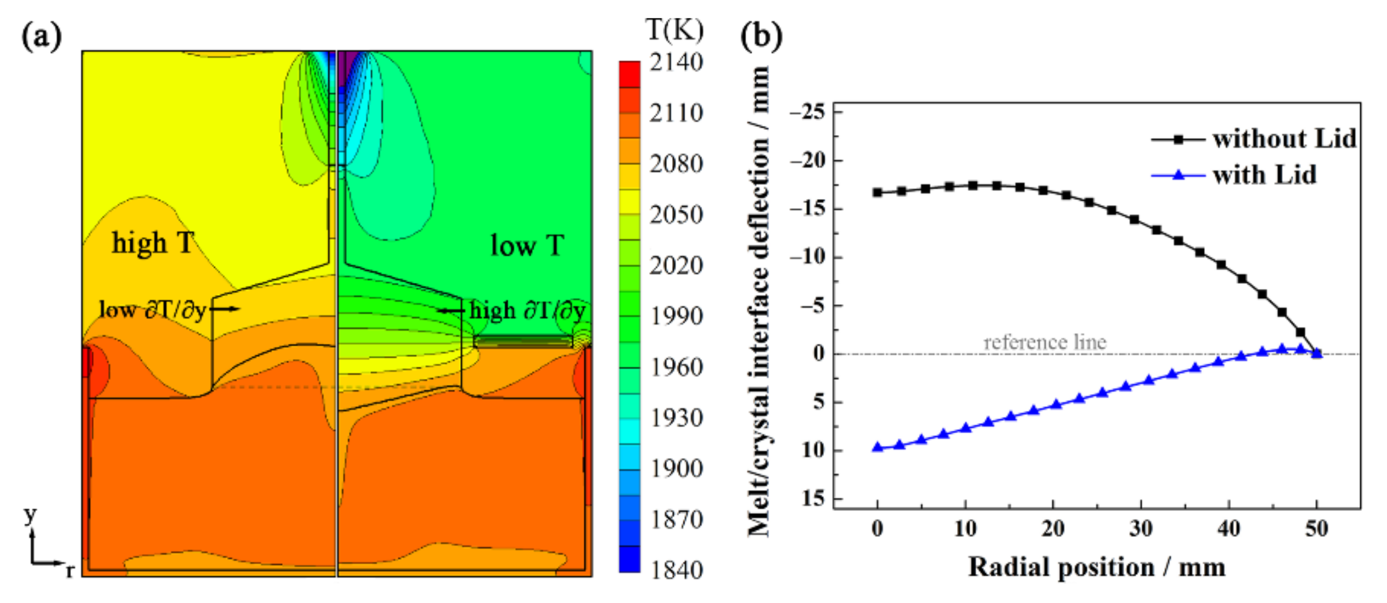
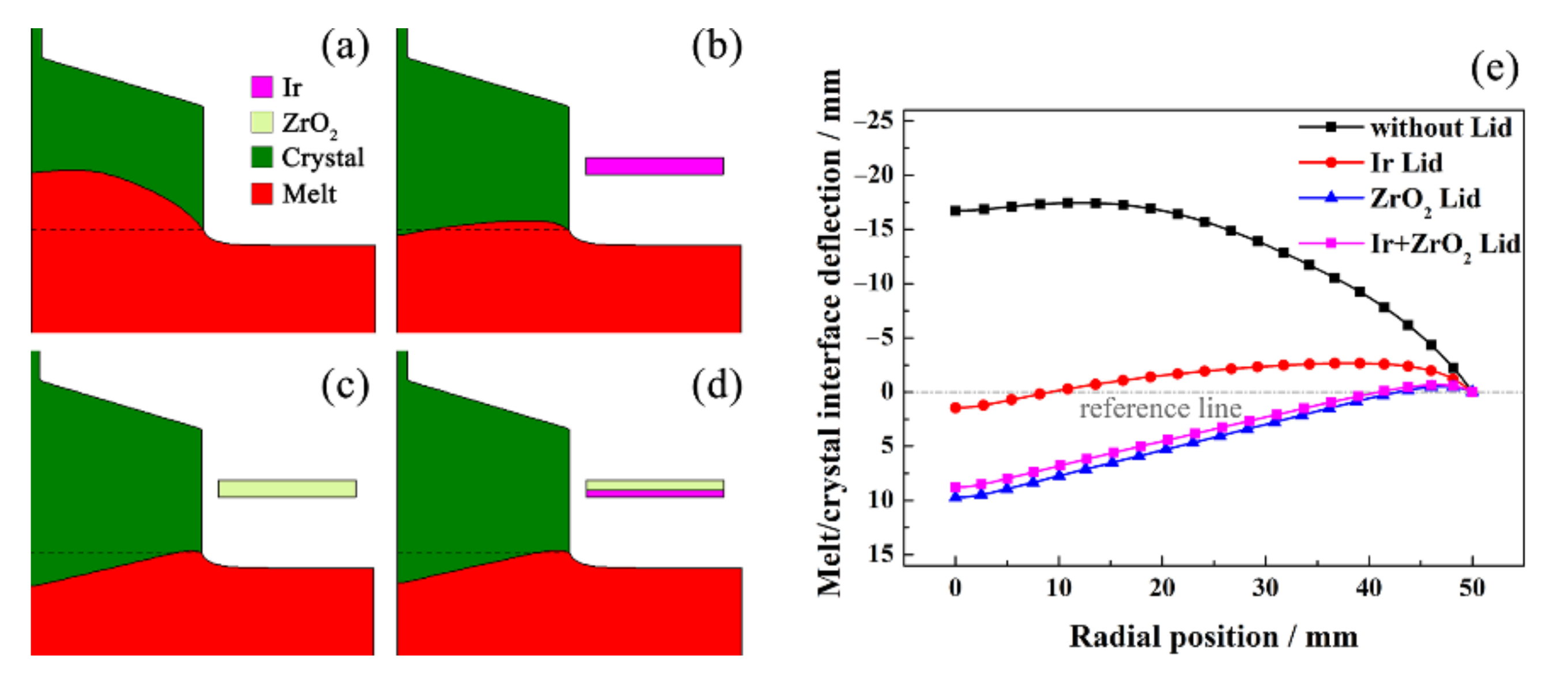
3.1. Effect of the Insulation Lid

Figure 2a compares the temperature distributions of the CZ system with and without the insulation lid, and their corresponding melt/crystal interface shapes are shown in Figure 2b. The insulation lid here is set as opaque and given a low thermal conductivity value (0.15 W∙m−1∙K−1) and an emissivity value (0.8), which are common in superior oxide insulation. The melt/crystal interface deflection is defined as the distance convex to the melt relative to the horizontal height of the triple point (shown as the reference line in Figure 2b). The melt/crystal interface in the CZ system without the insulation lid shows an obviously concave shape, but the one with the insulation lid shows a significantly convex shape, which is conducive to suppressing spiral growth and promoting crystal growth. It should be mentioned that the crystal is assumed to be opaque in the present work, which is the worst case for heat dissipation at the melt/crystal interface. Galazka et al. [9,11] reported that high free electron concentration will lead to low transmittance in the NIR spectral region and is not conductive to removing the latent heat of crystallization from the growth interface. This indicates that the insulation lid can still make the melt/crystal interface convex even for a 4-inch β-Ga2O3 single crystal with a high free electron concentration.
As shown in the left side of Figure 2a, for the CZ system without the insulation lid, the temperature is relatively uniform and high in all the space above the melt; thus, the crystal exhibits a low axial temperature gradient T / y , leading to a low growth velocity V crys and a concave shape of the melt/crystal interface. Axis y is set to be consistent with a symmetry axis orientation. Nevertheless, as shown in right side of Figure 2a, the insulation lid hinders upward heat transfer from the melt and crucible and significantly lowers the temperature in the space above the insulation lid. For this reason, the crystal shows a high axial temperature gradient T / y , leading to a high growth velocity V crys and a convex shape of the melt/crystal interface.

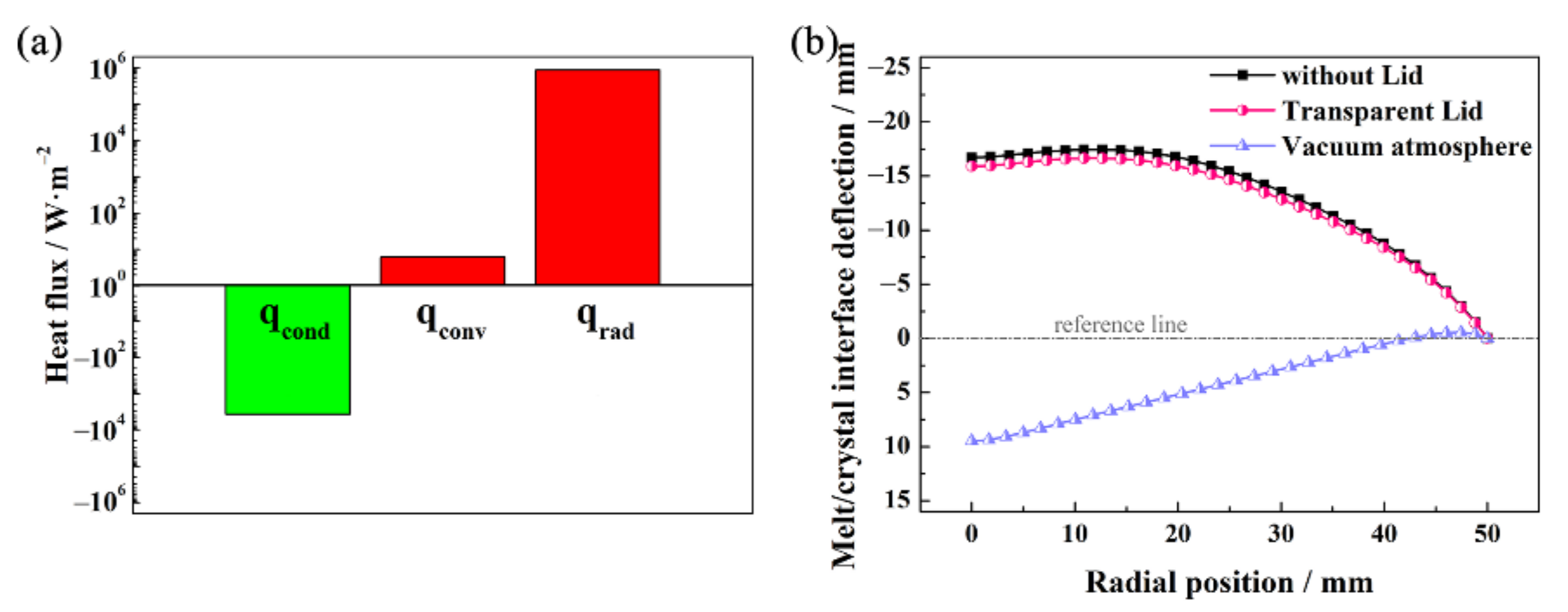
3.2. Heat Transfer Analysis

As mentioned above, hindering upward heat transfer from the melt and crucible is the key for the positive effect of the insulation lid. As we all know, there are three heat transfer modes: thermal conduction, thermal convection, and thermal radiation. Thus, it is necessary to clarify the concrete effect of the insulation lid on different heat transfer modes. The heat is mainly transferred from the bottom up, so the undersurface of the insulation lid is selected for heat transfer analysis. Figure 3a shows the average heat flux of thermal conduction (qcond), thermal convection (qconv), and incoming thermal radiation (qrad) on the undersurface of the insulation lid. Obviously, qrad and qconv are positive values, and qrad is five orders of magnitude larger than qconv, which means radiant heat is dominant in the heat hindered by the insulation lid. The qcond is a negative value because a portion of heat is lost by thermal conduction of the insulation lid. We have made three groups of confirmatory simulations to verify the correctness of the above conclusion. In one group, the insulation lid is set as transparent to allow radiant heat to pass through. Oppositely, in the other group, the atmosphere is set as a vacuum to make sure the insulation lid can only receive radiant heat from external objects. The group without the lid is set as the control group. Figure 3b shows the melt/crystal interface shapes in the groups without the lid and with the transparent lid. Both of them are almost the same, but they are quite different from the group within the vacuum atmosphere, which is also very close to the curve shape of the one with the lid in Figure 2b. This indicates that hindering radiant heat is the cause of the melt/crystal interface being convex, which well verifies the conclusion above.

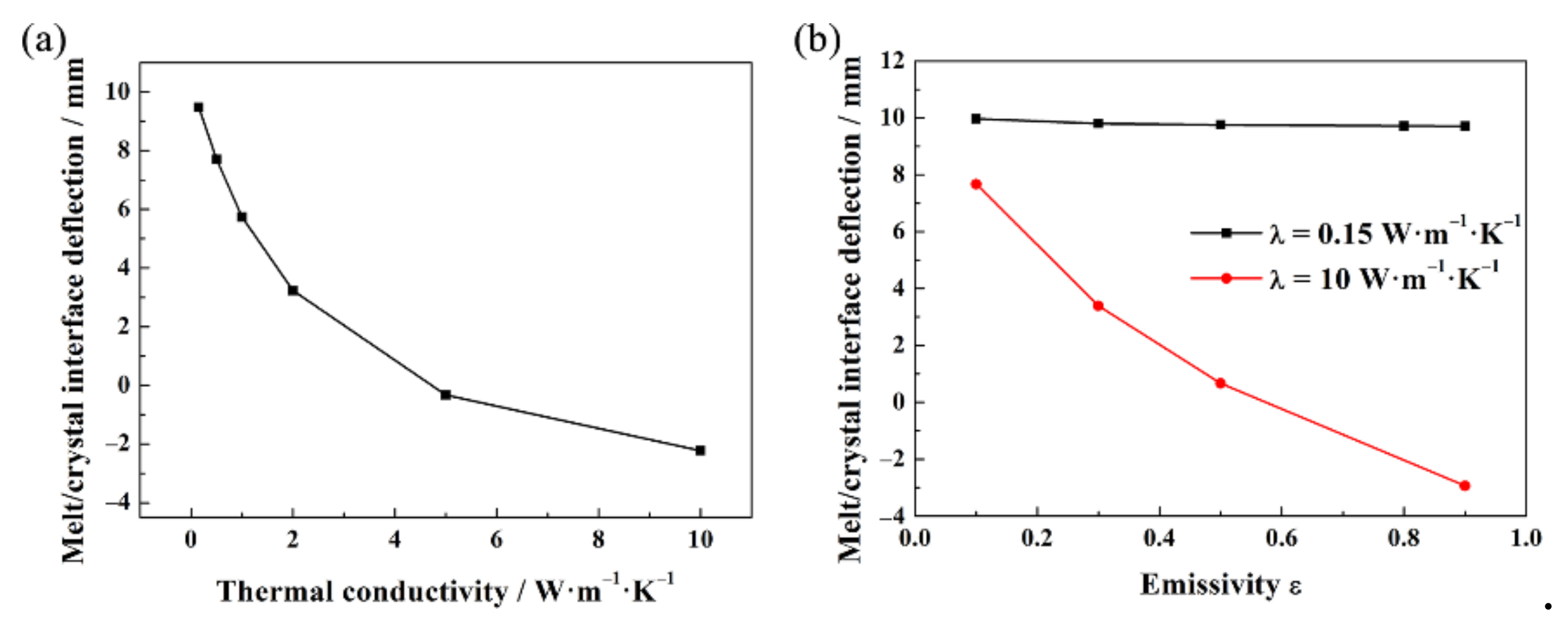
3.3. Material Parameters Selection

As shown in Formula (10) of Section 2.2, the radiation intensity I rad can be described by two parts; 1 ε q rad inc π is the reflected radiation intensity, and ε σ T 4 is the emission radiation intensity of the insulation lid, both of which determine the radiant intensity. Therefore, when the insulation lid is opaque, the I r a d of the insulation lid reflects the amount of radiant heat hindered by the insulation lid. According to Formula (10), when the incident radiative heat flux q rad inc is a certain value, I rad is dependent on the emissivity ε and the temperature T on the undersurface of the insulation lid. The surface temperature T is directly related to the thermal conductivity λ of the insulation lid: the lower the λ , the higher the T. Figure 4a shows the curves of the melt/crystal interface deflection versus the λ of the insulation lid. The melt/crystal interface deflection decreases with the increase of the λ because a larger λ will cause more heat loss by thermal conduction of the insulation lid and lower T on the undersurface of the insulation lid, leading to a smaller I rad . Figure 4b shows the curves of the melt/crystal interface deflection versus the ε of the insulation lid with both low and high λ . The melt/crystal interface deflection has no obvious change with the enhancement of the ε when λ is as low as 0.15 W∙m−1∙K−1. This is because that the radiant heat can hardly transfer upward due to the low λ of the insulation lid and is transferred back by the emission radiation of the insulation lid, leading to a high temperature gradient in the crystal. Comparatively, the melt/crystal interface deflection decreases with the enhancement of the ε when λ is as high as 10 W∙m−1∙K−1. This is because that the lower ε is, the more the radiant heat is transferred back by the reflected radiation of insulation lid undersurface. Therefore, in order to form a convex interface, the insulation lid needs to be composed of materials with low λ and low ε .
The insulation lid should be made of materials suited to an oxygen-containing atmosphere at high temperatures due to the harsh environments of β-Ga2O3 single crystal growth. Ir metal and ZrO2 material are the preferred materials for making the insulation lid. Figure 5 shows the effects of insulation lids made of different materials. The values of ε and λ refer to the physical property parameters of common commercial materials: 147 W∙m−1∙K−1 and 0.3 for Ir metal, and 0.15 W∙m−1∙K−1 and 0.8 for ZrO2 material. As shown in Figure 5b–e, the melt/crystal interface with the applied ZrO2 lid is more convex than the one for the applied Ir lid, indicating that a ZrO2 lid can isolate more heat than an Ir lid, which is conducive to scaling up the crystal diameter and suppressing spiral growth. However, the ZrO2 lid is at risk of cracking and dropping into the melt at high temperatures, so it has to be applied with Ir metal. Figure 5d shows a structure of a 3 mm thick ZrO2 lid connected concentrically with a 2 mm thick Ir lid below. The melt/crystal interface has a convex shape and is very close to the one seen with the applied ZrO2 lid. Therefore, the Ir lid + ZrO2 lid is the optimum selection. In addition, all the lids in Figure 5b–d are effective in solving the concave interface problem compared to not using a lid.

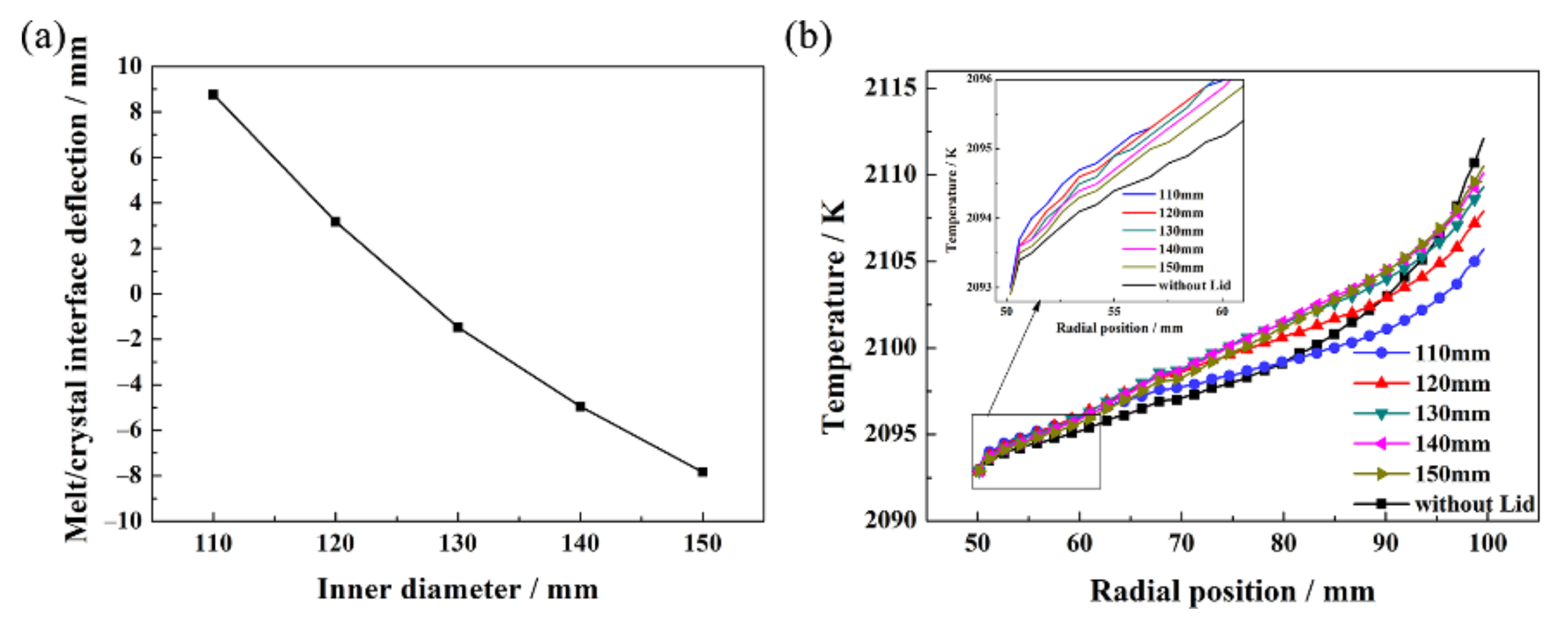
3.4. Effect of Inner Diameter

The insulation lid is circular structure, with an inner hole allowing the seed and crystal to pass through, so the inner diameter D in has a great influence on the isolation of radiant heat. In order to determine the size of the D in , the relationship between the D in and the interface deflection was studied, as shown in Figure 6a. The melt/crystal interface deflection decreases with the increase of the D in because more radiant heat is lost by passage through the inner hole. When the D in increases to 130 mm, the melt/crystal interface deflection decreases to negative value, and the interface becomes concave in shape. Therefore, the D i n should not be larger than 130 mm in this case. Figure 6b shows radial temperature distributions in the presence of insulation lids with different D in values, and the slope of each curve represents the corresponding radial temperature gradient at the melt’s free surface.
The radial temperature gradient decreases with the increase of the D in , which is beneficial to a more stable control of the crystal diameter and helps avoid the poly-crystallization caused by the fast expansion of the crystal diameter. Furthermore, all the temperatures with an insulation lid on the crucible wall (radial position = 100 mm) are lower than the one without an insulation lid, which is conducive to suppressing the decomposition of the Ga2O3 melt and the corrosion of the crucible.

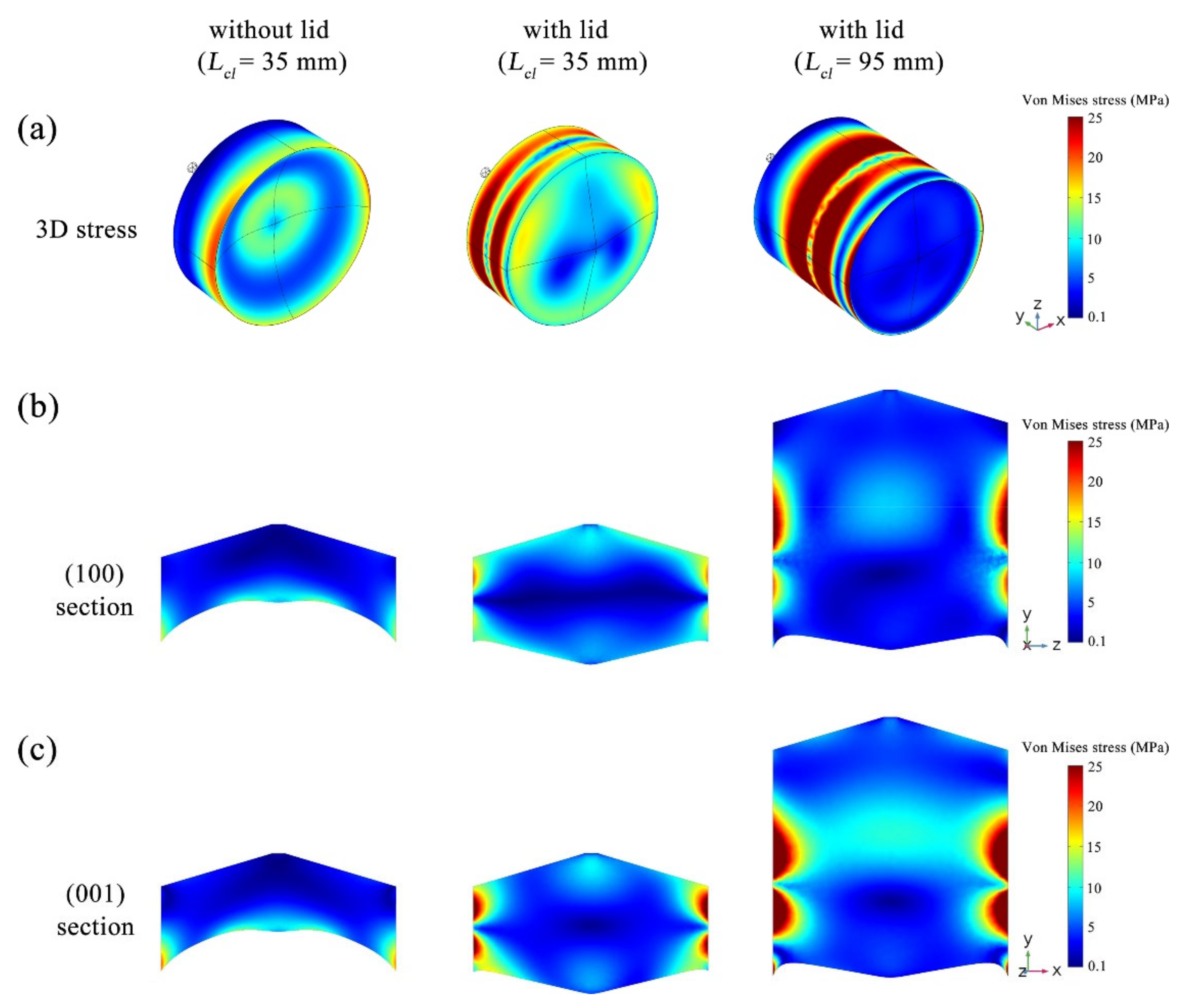
3.5. Thermal Stress Analysis

The high axial temperature gradient T / y in the crystal caused by the insulation lid can improve the shape of the melt/crystal interface, but it also brings a risk of increasing thermal stress. In this section, all physical properties and orientations discussed refer to the Cartesian reference system shown in Figure 7a. Axes y and z are parallel to the [010] and [001] crystal orientations, respectively, and the pulling direction of the crystal is parallel to axis y. Axis x is perpendicular to the (100) facet but not parallel to the [100] crystal orientations, which are parallel to the axis x* and have an angle of 103.7° to axis z [29]. β-Ga2O3 has two cleavage planes parallel to {100} and {001}. In order to show the 3D stress distribution inside the crystal, two cross sections parallel to the (100) and (001) facets are taken, as shown in Figure 7b.
Figure 8 compares the Von Mises stress distributions in crystals which are grown without or with an insulation lid. The distributions of those with an insulation lid are also shown, with the crystal length L c l = 35 mm and 95 mm, respectively. The crystal length L c l here is defined as the axial length from the shoulder position where the constant diameter growth started to the triple point. For the crystal grown without insulation lid, the stress inside the crystal is small because the temperature gradient is low because of the low T / y , as shown in Figure 2a. However, obvious stress concentration appeared in the center of the melt/crystal interface and the position near the triple point. This may lead to more dislocation multiplication and reduce the effective area of the wafer. For the crystal grown with an insulation lid, stress mainly concentrated on the crystal surface, especially on the surface close to the insulation lid, but the stress shows no significant increase inside the crystal. According to the distribution in the (100) section, there is stress concentration near the center of the melt/crystal interface and on the shoulder. However, on the melt/crystal interface, stress distributes lower in the center and higher in the outer edge, and the stress in the center is reduced compared with the crystal made without a lid. As the crystal grows to 95 mm in length, the stress on the melt/crystal interface and the shoulder decreases significantly and is basically distributed only at the outer edge. This indicates that the insulation lid will cause a better stress distribution, which inhibits dislocation multiplication in the center of the cylindrical crystal and will increase the effective area of the wafer.

4. Conclusions

The effect of an insulation lid on 4-inch β-Ga2O3 single crystals growth by the Czochralski method is analyzed by numerical simulation. The insulation lid can hinder upward radiant heat transfer from the melt and crucible and increase the axial temperature gradient in a crystal. As such, the use of the insulation lid makes the melt/crystal interface form a convex shape, which is conducive to suppressing spiral growth and promoting crystal growth. This indicates that the insulation lid can provide a favorable temperature distribution for 4-inch β-Ga2O3 single crystal growth, even with a high free electron concentration. Selecting the appropriate materials and size of the insulation lid is not only conducive to making the melt/crystal interface convex, but also facilitates better suppression of Ga2O3 melt decomposition and crucible corrosion. The insulation lid will also cause a better stress distribution, which inhibits dislocation multiplication in the center of the crystal and increases the effective area of the wafer. Taken together, adding an insulation lid may be a feasible idea for the growth of high-quality, 4-inch β-Ga2O3 single crystals by the Czochralski method.

Author Contributions

Conceptualization, D.W.; methodology, D.W., N.X.; software, D.W., N.X. and H.Z.; validation, K.M., J.W., C.L. and Z.J.; formal analysis, H.Z.; writing—original draft preparation, D.W.; writing—review and editing, N.X. and H.Z.; supervision, D.Y. All authors have read and agreed to the published version of the manuscript.

Funding

This research was funded by the National Natural Science Foundation of China (51871200, 22205203), National Program for Support of Top-notch Young Professionals, Fundamental Research Funds for the Central Universities (226-2022-00200), Foundation for Innovative Research Groups of the National Natural Science Foundation of China (61721005), and National Postdoctoral Program for Innovative Talents (BX20220264).

Data Availability Statement

Not applicable.

Conflicts of Interest

The authors declare no conflict of interest.

References

  1. Mu, W.; Jia, Z.; Yin, Y.; Fu, B.; Zhang, J.; Zhang, J.; Tao, X. Solid–liquid interface optimization and properties of ultra-wide bandgap β-Ga2O3 grown by Czochralski and EFG methods. CrystEngComm 2019, 21, 2762–2767. [Google Scholar] [CrossRef]
  2. Jin, Z.; Liu, Y.Y.; Xia, N.; Guo, X.W.; Hong, Z.J.; Zhang, H.; Yang, D.R. Wet etching in β-Ga2O3 bulk single crystals. CrystEngComm 2022, 24, 1127–1144. [Google Scholar] [CrossRef]
  3. Higashiwaki, M.; Konishi, K.; Sasaki, K.; Goto, K.; Nomura, K.; Thieu, Q.T.; Togashi, R.; Murakami, H.; Kumagai, Y.; Monemar, B.; et al. Temperature-dependent capacitance–voltage and current–voltage characteristics of Pt/Ga2O3 (001) Schottky barrier diodes fabricated on n-Ga2O3 drift layers grown by halide vapor phase epitaxy. Appl. Phys. Lett. 2016, 108, 133503. [Google Scholar] [CrossRef]
  4. He, Q.; Mu, W.; Fu, B.; Jia, Z.; Long, S.; Yu, Z.; Yao, Z.; Wang, W.; Dong, H.; Qin, Y.; et al. Schottky Barrier Rectifier Based on (100) β-Ga2O3 and its DC and AC Characteristics. IEEE Electron Device Lett. 2018, 39, 556–559. [Google Scholar] [CrossRef]
  5. Luchechko, A.; Vasyltsiv, V.; Kostyk, L.; Tsvetkova, O.; Popov, A.I. Shallow and deep trap levels in X-ray irradiated β-Ga2O3: Mg. Nucl. Instrum. Methods Phys. Res. Sect. B Beam Interact. Mater. At. 2019, 441, 12–17. [Google Scholar] [CrossRef]
  6. Tang, X.; Liu, B.; Yu, Y.; Song, B.; Han, P.; Liu, S.; Gao, B. Effect of Internal Radiation on Process Parameters in the Global Simulation of Growing Large-Size Bulk β-Ga2O3 Single Crystals with the Czochralski Method. Crystals 2021, 11, 763. [Google Scholar] [CrossRef]
  7. Tomm, Y.; Reiche, P.; Klimm, D.; Fukuda, T. Czochralski grown Ga2O3 crystals. J. Cryst. Growth 2000, 220, 510–514. [Google Scholar] [CrossRef]
  8. Galazka, Z.; Uecker, R.; Irmscher, K.; Albrecht, M.; Klimm, D.; Pietsch, M.; Brützam, M.; Bertram, R.; Ganschow, S.; Fornari, R. Czochralski growth and characterization of β-Ga2O3 single crystals. Cryst. Res. Technol. 2010, 45, 1229–1236. [Google Scholar] [CrossRef]
  9. Galazka, Z.; Irmscher, K.; Uecker, R.; Bertram, R.; Pietsch, M.; Kwasniewski, A.; Naumann, M.; Schulz, T.; Schewski, R.; Klimm, D.; et al. On the bulk β-Ga2O3 single crystals grown by the Czochralski method. J. Cryst. Growth 2014, 404, 184–191. [Google Scholar] [CrossRef]
  10. Galazka, Z.; Uecker, R.; Klimm, D.; Irmscher, K.; Naumann, M.; Pietsch, M.; Kwasniewski, A.; Bertram, R.; Ganschow, S.; Bickermann, M. Scaling-Up of Bulk β-Ga2O3 Single Crystals by the Czochralski Method. ECS J. Solid State Sci. Technol. 2016, 6, Q3007–Q3011. [Google Scholar] [CrossRef]
  11. Galazka, Z. Growth of bulk β-Ga2O3 single crystals by the Czochralski method. J. Appl. Phys. 2022, 131, 031103. [Google Scholar] [CrossRef]
  12. Liu, Y.; Guo, X.; Xia, N.; Hong, Z.; Zhang, H.; Yang, D. Floating Particles in the Melt during the Growth of β-Ga2O3 Single Crystals Using the Czochralski Method. Metals 2022, 12, 1171. [Google Scholar] [CrossRef]
  13. Aida, H.; Nishiguchi, K.; Takeda, H.; Aota, N.; Sunakawa, K.; Yaguchi, Y. Growth of β-Ga2O3 Single Crystals by the Edge-Defined, Film Fed Growth Method. Jpn. J. Appl. Phys. 2008, 47, 8506–8509. [Google Scholar] [CrossRef]
  14. Mastro, M.A.; Kuramata, A.; Calkins, J.; Kim, J.; Ren, F.; Peartong, S.J. Opportunities and Future Directions for Ga2O3. ECS J. Solid State Sci. Technol. 2017, 6, P356–P359. [Google Scholar] [CrossRef]
  15. Kuramata, A.; Koshi, K.; Watanabe, S.; Yamaoka, Y.; Masui, T.; Yamakoshi, S. Bulk Crystal Growth of Ga2O3. Proc. SPIE 2018, 10533, 9–14. [Google Scholar] [CrossRef]
  16. Fu, B.; Mu, W.; Zhang, J.; Wang, X.; Zhuang, W.; Yin, Y.; Jia, Z.; Tao, X. A study on the technical improvement and the crystalline quality optimization of columnar β-Ga2O3 crystal growth by an EFG method. CrystEngComm 2020, 22, 5060–5066. [Google Scholar] [CrossRef]
  17. Hoshikawa, K.; Ohba, E.; Kobayashi, T.; Yanagisawa, J.; Miyagawa, C.; Nakamura, Y. Growth of β-Ga2O3 single crystals using vertical Bridgman method in ambient air. J. Cryst. Growth 2016, 447, 36–41. [Google Scholar] [CrossRef]
  18. Hoshikawa, K.; Kobayashi, T.; Ohba, E. 50 mm diameter Sn-doped (001) β-Ga2O3 crystal growth using the vertical Bridgeman technique in ambient air. J. Cryst. Growth 2020, 546, 125778. [Google Scholar] [CrossRef]
  19. Villora, E.G.; Shimamura, K.; Yoshikawa, Y.; Aoki, K.; Ichinose, N. Large-size β-Ga2O3 single crystals and wafers. J. Cryst. Growth 2004, 270, 420–426. [Google Scholar] [CrossRef]
  20. Suzuki, N.; Ohira, S.; Tanaka, M.; Sugawara, T.; Nakajima, K.; Shishido, T. Fabrication and characterization of transparent conductive Sn-doped β-Ga2O3 single crystal. Phys. Status Solidi C 2007, 4, 2310–2313. [Google Scholar] [CrossRef]
  21. Galazka, Z.; Ganschow, S.; Reiche, P.; Uecker, R. Experimental Study of Interface Inversion of Tb3ScxAl5−xO12 Single Crystals Grown by the Czochralski Method. Cryst. Res. Technol. 2002, 37, 407–413. [Google Scholar] [CrossRef]
  22. Derby, J.J.; Brown, R.A. Thermal-capillary analysis of Czochralski and liquid encapsulated Czochralski crystal growth: I. Simulation. J. Cryst. Growth 1986, 74, 605–624. [Google Scholar] [CrossRef]
  23. Song, D.W.; Lee, S.H.; Mun, Y.H.; Kim, H. Oxygen content increasing mechanism in Czochralski (CZ) silicon crystals doped with heavy antimony under a double-typed heat shield. J. Cryst. Growth 2011, 325, 27–31. [Google Scholar] [CrossRef]
  24. Teng, R.; Zhou, Q.G.; Dai, X.L.; Wu, Z.Q.; Xu, W.T.; Xiao, Q.H.; Wu, X.; Guo, X. Optimization of heat shield for single silicon crystal growth by using numerical simulation. Rare Met. 2012, 31, 489–493. [Google Scholar] [CrossRef]
  25. Fang, H.S.; Pan, Y.Y.; Zheng, L.L.; Zhang, Q.J.; Wang, S.; Jin, Z.L. To investigate interface shape and thermal stress during sapphire single crystal growth by the Cz method. J. Cryst. Growth 2013, 363, 25–32. [Google Scholar] [CrossRef]
  26. Fang, H.S.; Tian, J.; Wang, S.; Long, Y.; Zhang, M.J.; Zhao, C.J. Numerical optimization of czochralski sapphire single crystal growth using orthogonal design method. Cryst. Res. Technol. 2014, 49, 323–330. [Google Scholar] [CrossRef]
  27. Fang, H.S.; Jin, Z.L.; Huang, X.M. Study and optimization of gas flow and temperature distribution in a Czochralski configuration. J. Cryst. Growth 2012, 361, 114–120. [Google Scholar] [CrossRef]
  28. Tang, X.; Liu, B.; Yu, Y.; Liu, S.; Gao, B. Numerical Analysis of Difficulties of Growing Large-Size Bulk β-Ga2O3 Single Crystals with the Czochralski Method. Crystals 2020, 11, 25. [Google Scholar] [CrossRef]
  29. Miller, W.; Böttcher, K.; Galazka, Z.; Schreuer, J. Numerical Modelling of the Czochralski Growth of β-Ga2O3. Crystals 2017, 7, 26. [Google Scholar] [CrossRef] [Green Version]
  30. Dingwell, D.B. Density of Ga2O3 Liquid. J. Am. Ceram. Soc. 1992, 75, 1656–1657. [Google Scholar] [CrossRef]
  31. Guo, Z.; Verma, A.; Wu, X.; Sun, F.; Hickman, A.; Masui, T.; Kuramata, A.; Higashiwaki, M.; Jena, D.; Luo, T. Anisotropic thermal conductivity in single crystal β-gallium oxide. Appl. Phys. Lett. 2015, 106, 111909. [Google Scholar] [CrossRef] [Green Version]
  32. Demina, S.E.; Bystrova, E.N.; Postolov, V.S.; Eskov, E.V.; Nikolenko, M.V.; Marshanin, D.A.; Yuferev, V.S.; Kalaev, V.V. Use of numerical simulation for growing high-quality sapphire crystals by the Kyropoulos method. J. Cryst. Growth 2008, 310, 1443–1447. [Google Scholar] [CrossRef]
  33. Kalaev, V.V.; Evstratov, I.Y.; Makarov, Y.N. Gas flow effect on global heat transport and melt convection in Czochralski silicon growth. J. Cryst. Growth 2003, 249, 87–99. [Google Scholar] [CrossRef]
Figure 1. Schematic diagram of CZ system for 4-inch β-Ga2O3 single crystal growth.
Crystals 12 01715 g001
Figure 2. (a) Temperature distributions of the CZ system. Left: without, and right: with insulation lid. (b) The corresponding melt/crystal interface shapes in (a).
Crystals 12 01715 g002
Figure 3. (a) Average heat flux of thermal conduction, thermal convection, and incoming thermal radiation on the undersurface of the insulation lid. (b) The melt/crystal interface shapes in CZ systems that without lid, with transparent lid, and within vacuum atmosphere.
Crystals 12 01715 g003
Figure 4. The curves of the melt/crystal interface deflection versus (a) thermal conductivity and (b) emissivity of the insulation lid.
Crystals 12 01715 g004
Figure 5. Simulation results of the CZ system (a) without an insulation lid, and with an insulation lid made of the following materials: (b) Ir, (c) ZrO2, and (d) Ir+ZrO2, respectively. (e) The corresponding melt/crystal interface shapes in (ad).
Crystals 12 01715 g005
Figure 6. The curve of (a) the melt/crystal interface deflection and (b) radial temperature distributions versus inner diameter D in of the insulation lid from 110 mm to 150 mm. The inset is an enlarged portion near the triple point.
Crystals 12 01715 g006
Figure 7. (a) Unit cell of β-Ga2O3 in standard coordinate system. (b) Schematic diagram of two cross sections in a cylindrical crystal.
Crystals 12 01715 g007
Figure 8. Von Mises stress distributions in crystals grown without an insulation lid, with an insulation lid (crystal length = 35 mm), and with an insulation lid (crystal length = 95 mm). (a) 3D distribution and plane distributions in (b) the (100) section and (c) the (001) section. The boundary condition of fixed constraint is added at the top surface of the seed.
Crystals 12 01715 g008
Table 1. Material properties of β-Ga2O3 melt and crystal [30,31].
PropertiesSymbolMeltCrystal
Densityρ (kg/m3)6217.35-0.65T5974.5-0.0815T
Specific heatCp (J∙kg−1∙K−1)850700
Thermal conductivityλ (W∙m−1∙K−1)4.332,800 × (1/T)1.27
Emissivityε0.50.3
Melting point Tm (K)/2093
Latent heatΔH (kJ/kg)533.5/
Viscosityμ (Pa∙s)0.05/
Publisher’s Note: MDPI stays neutral with regard to jurisdictional claims in published maps and institutional affiliations.

