Article

Demonstration of III-Nitride Red LEDs on Si Substrates via Strain-Relaxed Template by InGaN Decomposition Layer

1
Materials Department, University of California, Santa Barbara, CA 93106, USA
2
Chemical Engineering Department, University of California, Santa Barbara, CA 93106, USA
3
Electrical and Computer Engineering Department, University of California, Santa Barbara, CA 93106, USA
*
Author to whom correspondence should be addressed.
Submission received: 30 July 2022 / Revised: 12 August 2022 / Accepted: 12 August 2022 / Published: 15 August 2022
(This article belongs to the Special Issue GaN-Based Materials and Devices)

Abstract

:
A III-nitride red LED with an active region temperature of 835 °C on a Si substrate utilizing a strain-relaxed template (SRT) is demonstrated. The peak wavelength blueshifts from 670 nm at 1 A/cm2 to 636 nm at 150 A/cm2. The on-wafer external quantum efficiency was 0.021% at 7 A/cm2 with an emission wavelength of 655 nm. The LED grown on a Si substrate exhibited a 116 nm redshift when compared to a co-loaded LED grown on sapphire. This is attributed to the difference in strain state for the III-nitride layers grown on Si compared to sapphire, allowing for more indium to be incorporated in the LED grown on Si. This suggests efficient III-nitride red LEDs and µLEDs on Si with a SRT can be realized with further material, device structure, and processing optimizations.

1. Introduction

Light emitting diodes (LEDs) are now widely favored over incandescent bulbs, liquid-crystal displays (LCDs) (which employ an LED backlight), organic LEDs (OLEDs), and other lighting sources in a plethora of applications, including displays, sensing, etc., due to their long operational lifetime, high efficiency, chemical inertness, and wide color gamut [1,2]. Micron-sized LEDs (µLEDs) are an emerging technology for more futuristic technologies, such as near-eye displays, portable technology, and visible light communication [2]. These LEDs and µLEDs are comprised of either III-nitride or III-phosphide material systems, where indium gallium nitride (InGaN) is used for blue and green, and aluminum gallium indium phosphide (AlGaInP) is used for red.
Although they are currently much more efficient than red-emitting InGaN-based devices [3,4,5,6], AlGaInP-based LEDs have several disadvantages and fundamental limitations for use as a red µLED. They have much higher surface recombination velocity and longer carrier diffusion length than III-nitrides [7], which leads to reduced external quantum efficiency (EQE) as the LED dimensions decrease [8]. The opposite trend has been observed in InGaN-based µLEDs, where the EQE increased with decreasing device size [9]. AlGaInP-based LEDs also have poor thermal stability at elevated current densities when compared to InGaN-based LEDs, limiting their ability to be employed in high brightness or high-temperature applications [10].
As mentioned previously, blue and green InGaN-based LEDs are readily obtainable, but the performance of red InGaN-based LEDs is significantly worse and still lags behind [11,12]. III-nitride red LEDs are challenging, in part, because red emission in this material system requires the indium (In) content in the emitting quantum wells (QWs) to be above 35% [13] and leads to increased strain and poor crystal quality due to the 11% lattice mismatch between indium nitride (InN) and gallium nitride (GaN) [14,15]. This increased compressive strain leads to reduced In incorporation [15]. The higher equilibrium vapor pressure of nitrogen over InN relative to the other III-nitrides [16,17] also requires lower growth temperatures for high In-content InGaN layers that are necessary for red III-nitride-based LEDs, which tends to lead to lower crystal quality and higher impurity concentration.
As such, many efforts exist to explore novel methods of achieving better crystal quality InGaN pseudo-substrates and more efficient III-nitride red LEDs [18,19,20,21,22]. Of the methods previously mentioned, they each require some degree of patterning and regrowth, which from a large-scale manufacturing perspective is very expensive and time-consuming. One novel method that has the potential to achieve efficient red III-nitride-based LEDs without any extra patterning or regrowth on entire wafers is through the use of InGaN strain-relaxed templates (SRT) [22,23]. In these reports, the LEDs include a 3 nm low-temperature high-In composition InGaN decomposition layer (DL). A subsequent region called the decomposition stop layer (DSL) is grown at a higher temperature to thermally decompose a portion of the high In content present in this layer to form voids, metallic In, and Ga [24]. After thermally decomposing the DL, increased In incorporation and within the InGaN buffer on the DSL with higher strain relaxation is observed. We call the DL, DSL, and InGaN buffer a SRT. This allows for higher metalorganic chemical vapor deposition (MOCVD) growth temperatures of InGaN layers compared to other methods, enabling a pathway to higher crystal quality InGaN films needed for efficient red µLEDs and red III-nitride LEDs.
As the second-most abundant element in Earth’s crust behind only oxygen, cost-effective, scalable, large, and high-purity wafers of silicon (Si) are readily available. Si has a small bandgap that absorbs the emitted light [25], and as a result, LEDs are typically grown on optically transparent substrates, such as sapphire, due to their higher light extraction efficiency. Furthermore, Si has a diamond cubic crystal structure, whereas the conventional III-nitrides have the wurtzite crystal structure. This lattice mismatch, in conjunction with different thermal properties [26,27], has made realizing high crystal quality GaN on Si templates difficult until recently [28], and recently, high-efficiency III-nitride-based yellow, orange, and red LEDs have been grown on Si substrates [29,30]. In fact, so much progress has been made that commercially available GaN on Si templates are available. GaN layers grown on Si are under biaxial tensile strain, while they are under compression when grown on sapphire [31,32]. Furthermore, there are established and advanced processing techniques for Si due to its widespread use in the photonics and electronics industries. As such, developing and improving LED performance on Si is especially interesting and worth exploring to allow III-nitride LEDs to penetrate even further into the general illumination market.
In this work, the first III-nitride red LED with a SRT grown on a Si substrate is demonstrated.

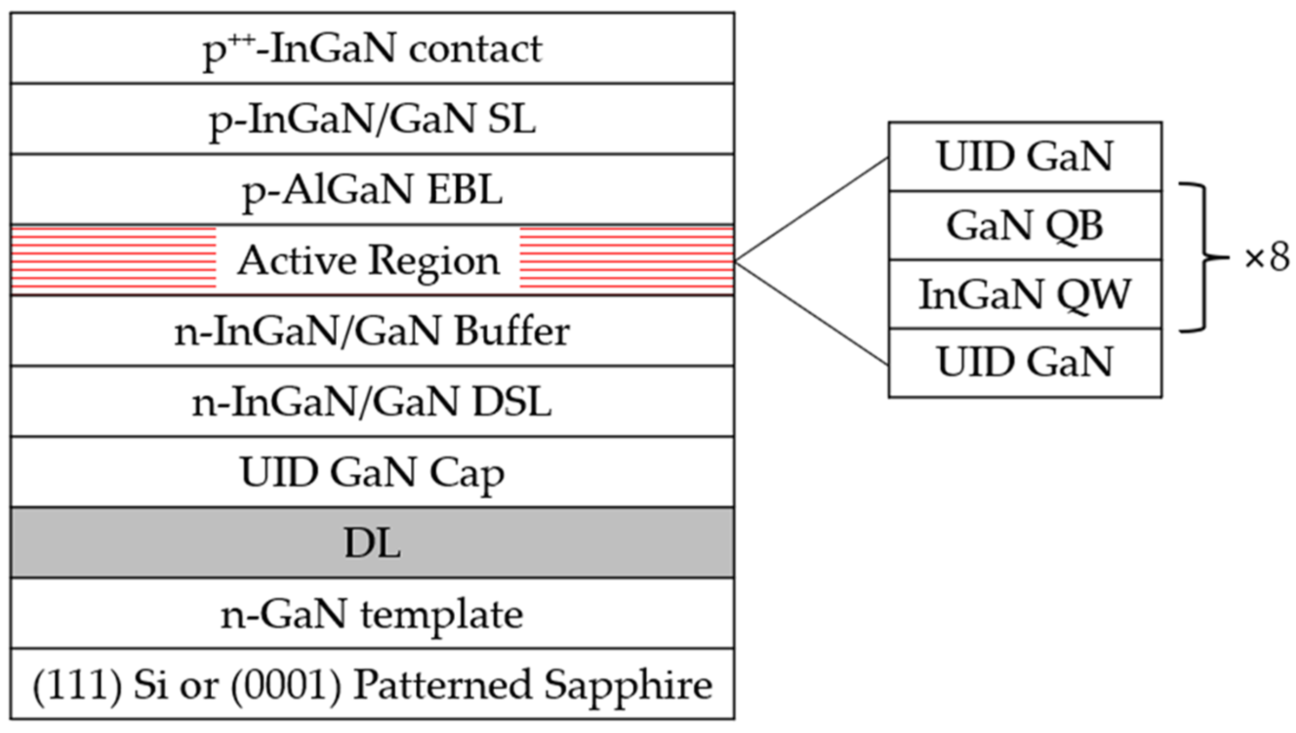
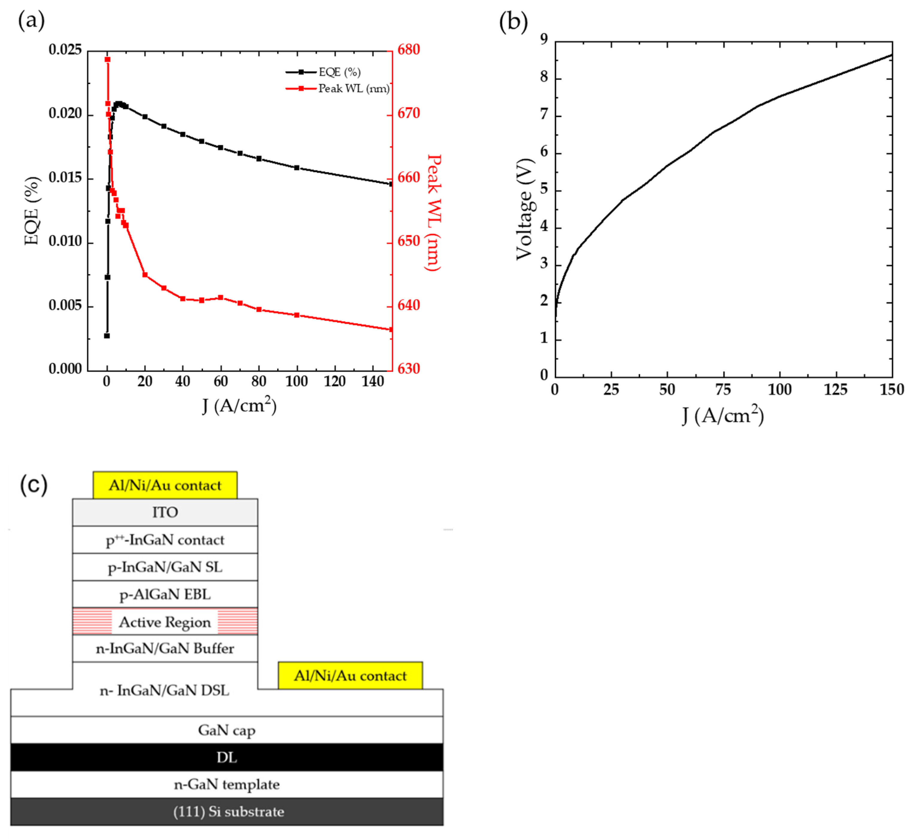
2. Materials and Methods

LEDs were grown by MOCVD on ½ 2” (0001) patterned sapphire substrate (PSS) and 13 by 13 mm (111) Si. The epitaxial structure is shown in Figure 1. The device structure of the processed LEDs on Si is the same as that depicted in Figure 1 of [23]. The GaN template was 8 and 7 µm thick for the PSS and Si substrates, respectively. A 2.6 nm unintentionally doped (UID) InGaN DL was grown at 720 °C on these templates. The DL was capped by 4 nm GaN at a relatively low temperature to prevent the InN in the DL from desorbing. A DSL consisting of a 10-period 7 nm n-InGaN/3 nm n-GaN superlattice (SL) was grown at 965 °C to decompose the DL, as described previously, and serves as a pseudo-substrate for subsequent LED growth. A 5-period 20 nm n-InGaN/2 nm n-GaN SL buffer grown at 935 °C served as the n-contact layer. The active region consisted of 5 nm UID GaN grown at 915 °C, an 8-period 2.5 nm InGaN/7 nm GaN multi-quantum well (MQW) structure at 835 °C, and a 5 nm UID GaN grown at 875 °C. Lastly, the p-side of the devices subsequently consisted of a 12 nm p+-AlGaN electron blocking layer (EBL), a 4-period 20 nm p-InGaN/2 nm p-GaN SL, and a 12 nm p++-InGaN contact layer grown at 935 °C. After growth, the LEDs were annealed at 600 °C for 20 min in air to activate the p-type layers.
After the MOCVD growth, In metal dots were pressed on the p-type layers and soldered on the sidewall of the wafers to allow for electrical probing of both LEDs grown on Si and PSS as a quick test. The PSS LEDs were probed at approximately the half-radius. Samples were then placed in aqua regia at 120 °C to etch the In metal off. A total of 110 nm of ITO was deposited using electron beam evaporation. Photolithography was used to pattern the samples. ITO was etched using CH4/H2/Ar reactive ion etching. A 0.1 mm2 mesa was formed by SiCl4 reactive ion etching to etch through the p-type and active regions and stop in the buffer region to create an n-contact. Lastly, 700 nm Al, 100 nm Ni, and 700 nm Au were deposited by electron beam evaporation to create a common metal n- and p-contact.
The LEDs were electrically probed under direct current (DC) conditions on-wafer underneath a 6-inch diameter Labsphere integrating sphere to obtain electrical and optical properties. A Horiba Jovin Yvon iHR320 series monochromator using a thermoelectrically cooled Synapse CCD was used to measure the EL spectra. The topside collection angle is approximately 180° normal to the substrate top surface, which, in conjunction with a fiber-coupled blackbody source HL-3P-INT-CAL radiometric calibration source from Ocean Insight, was used to calibrate the system. The method for calculating EQE is similar to the procedure reported in [33]. Pulsed measurements were made using a pulse generator with a pulse width of 5 µs and a 5% duty cycle. The EL spectrum was collected with an Ocean-Optics spectrometer connected to an optical fiber.

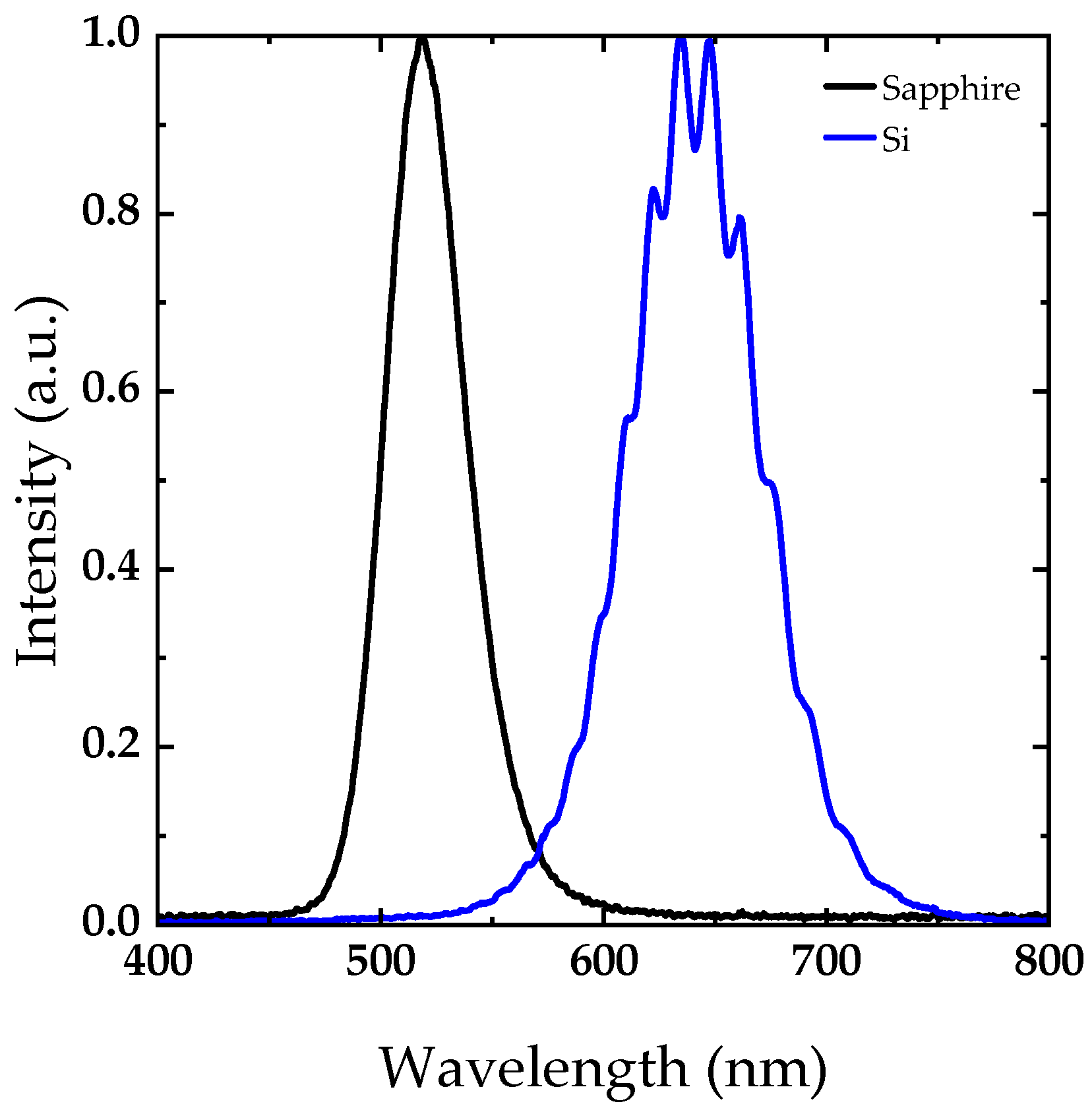
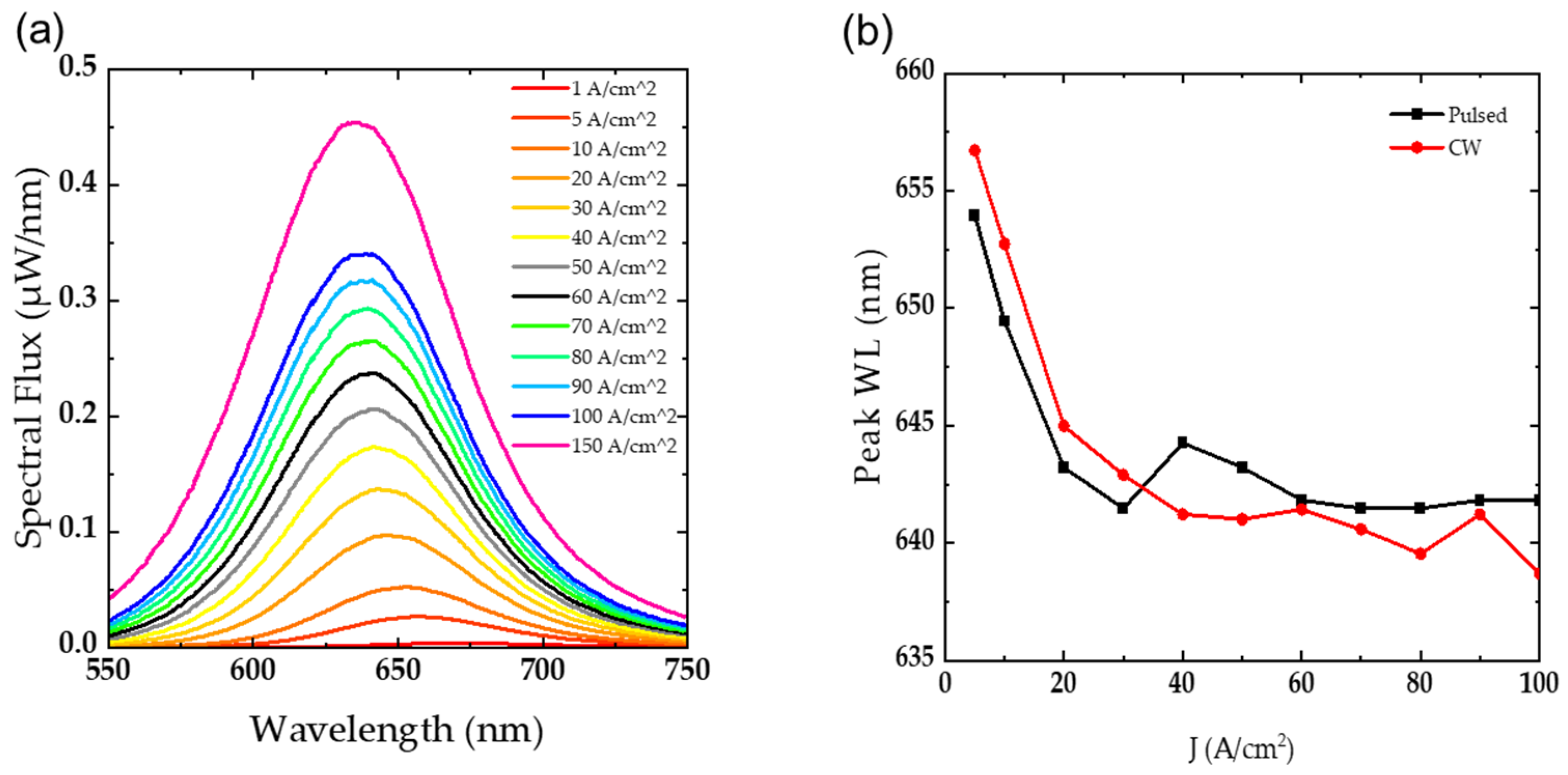
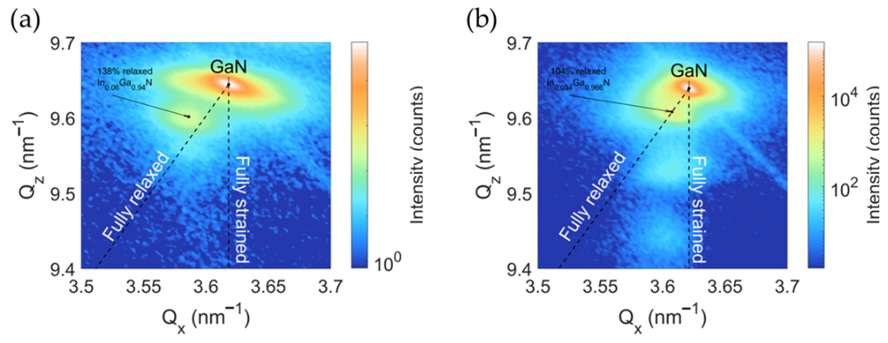
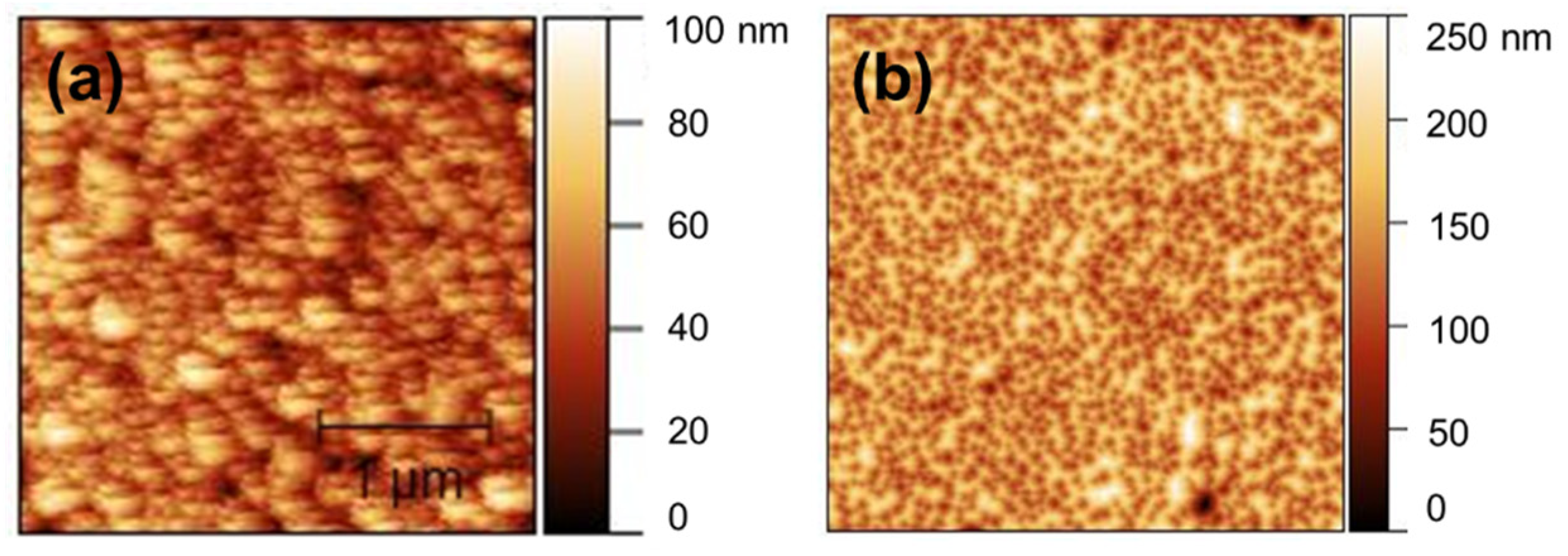
3. Results and Discussion

The EL-normalized spectra at 20 mA obtained by the quick test are shown in Figure 2 for the co-loaded LEDs. The black curve corresponds to the LED grown on PSS, while the blue curve was from the Si. The PSS had a peak wavelength of 519 nm. Its FWHM was 42 nm. Interestingly, Si had a peak wavelength of 635 nm. This is at least a 116 nm redshift when compared to the peak wavelengths of the co-loaded LEDs grown on PSS. The FWHM was 66 nm. The fringes present on the Si substrate spectra are attributed to the presence of a standing wave at the GaN/Si interface and are artifacts of the measurement setup, which is verified below when discussing the processed LEDs. Not only does utilizing a SRT lead to a redshift compared to reference LEDs grown without a SRT [23], but growing the SRT LEDs on a Si substrate leads to an additional redshift compared to PSS.
The on-wafer calibrated spectral flux of SRT LEDs on Si after the device processing at different current densities ranging from 1 to 150 A/cm2 is shown in Figure 3a. There are no fringes with this measurement setup because of the use of an integrating sphere. The LEDs turned on at 0.4 A/cm2 with a peak wavelength of 679 nm. The peak wavelength blueshifted 34 nm from 670 nm at 1 A/cm2 to 636 nm at 150 A/cm2. This blueshift is due to the polar c-plane orientation of the LEDs and is due to polarization screening of the MQW electric field or band-filling effects of the localized state [34,35,36]. The peak wavelength (WL) of the red LEDs grown on the Si substrate was measured under pulsed and DC operation as a function of current density to study thermal effects, as shown in Figure 3b. The blueshift from 5 to 100 A/cm2 under pulsed and DC operation is 12 and 18 nm, respectively. Thus, the redshift caused by the thermal effects under DC operation should be small. The large compositional fluctuations in the active layer of the red LED, as mentioned in Figure 3a, form localized states that contribute to longer wavelength emission at low current densities. With increasing current density, the blueshift of the peak WL is a result of band-filling effects of these localized states. The blueshift observed over this current density range is less than previous SRT demonstrations [12,23] and similar to other red III-nitride LED demonstrations [4,30,37]. The FWHM ranged from 64 nm at 1 A/cm2 to 84 nm at 150 A/cm2. At 20 A/cm2, the peak wavelength and FWHM were 645 and 69 nm, respectively. These FWHM values are comparable to previous demonstrations of red LEDs using SRT technology [12,23] but relatively high compared to other red III-nitride LEDs [30,37,38] and an indication that further growth optimizations must be looked into. The large FWHM for red III-nitride LEDs is due to indium compositional fluctuations in the active region, and the increase in FWHM as current density increases is attributed to heating effects that lead to the filling of higher energy states [37,39].
Figure 4a shows the EQE and peak WL as a function of current density, while Figure 4b shows the J-V characteristics. The on-wafer peak EQE was 0.021% at 7 A/cm2 and emitted at a wavelength of 655 nm. The peak EQE is low compared to those devices grown on transparent sapphire substrates [12,37,38,40] because Si is a highly absorbing substrate, and the DL has metallic In and Ga that also strongly absorb emitted light; a cross-sectional schematic of the fully processed LED is shown in Figure 4c. Most of the light absorption is due to the 1-mm thick Si substrate [41,42]. The presence of In and Ga metallic clusters is expected to be the primary source of light absorption in the DL, but since the DL is only 2.6 nm thick, this contribution should be small. TEM images show that these In and Ga metallic clusters are, in fact, present in our LEDs [22]. Other red LEDs epitaxially grown on Si with better EQEs employ a film transfer technique with a reflective backside coating, which prevents the Si substrate from absorbing light, thus greatly enhancing the light extraction efficiency [30,43]. Additionally, SRT LEDs have dislocations formed during the growth of the DSL, which is what allows for the relaxation of the InGaN layers. These dislocations act as nonradiative recombination centers for carriers, further reducing the EQE. Droop is observed at higher current densities and is attributed to carrier overflow [44] or Auger recombination [45]. To improve the EQE, a flip-chip architecture with reflective contacts and Si substrate removal can be incorporated. At 0.4, 1, and 5 A/cm2, the voltage is 1.9, 2.1, and 2.9 V, respectively. These values are lower or comparable to other red III-nitride LEDs [30,46,47], an indication that LEDs utilizing a SRT may be ideal for µLEDs, which are expected to have operating current densities in this range. The voltage at a high current density of 20 A/cm2 is a relatively high 4.1 V, but it turns on at a much lower current density [4]. These high voltages at this high current density can be attributed to poor current spreading and hole injection into the active region due to low p-InGaN conductivity and a large device size [48].
High-resolution X-ray diffraction (XRD) reciprocal space maps (RSMs) of the (10–15) off-axis peaks for samples on sapphire and Si substrates were taken with a Rigaku Hypix 2000 to measure and analyze the strain state and estimate the equivalent In composition of the InGaN/GaN SL buffer region, which is depicted in Figure 5. As shown, the InGaN buffer peak is offset in Qx relative to the GaN peak for both samples, indicating that the InGaN buffer is not coherently strained to the GaN template and the in-plane lattice constants of these two regions are different. This reduces the compositional pulling effect [17], allowing the LEDs to be grown at hotter temperatures than other methods while still incorporating enough In for red emission in the QWs. The equivalent buffer composition and relaxation for the LEDs grown on Si and sapphire were 138% relaxed In0.06Ga0.94N and 104% relaxed In0.034Ga0.966N, respectively. Relaxation values calculated to be over 100% indicate that the nominally compressed buffer region is actually under biaxial tensile strain. This biaxial tension allows for more In to be incorporated in the epitaxial structure of the LED grown on Si than the one grown on sapphire. As mentioned previously, heteroepitaxial GaN on sapphire is compressively strained while GaN on Si is tensile strained [28,29,30,31,32]. This tensile GaN grown on Si will have a longer in-plane a lattice parameter than the compressive GaN on sapphire. When leveraging this with SRT technology, the InGaN buffer grown on Si is more relaxed and then tensile strained (138%), while the InGaN buffer grown on PSS is less relaxed (104%), as shown in Figure 5. The increased relaxation allows for more indium incorporation into InGaN during MOCVD growth by minimizing the compositional pulling effect [17]. This accounts for the larger redshift of the red LEDs grown on Si than those on PSS. The mechanism responsible for the presence of tensile strain in typically compressive InGaN layers is hypothesized to be the result of inclined threading dislocations that have a misfit component when projected onto the growth plane and to the best of the authors’ knowledge, has only been observed in the III-nitride material system when growing aluminum gallium nitride (AlGaN) films [49,50,51,52,53] and not InGaN layers. Further analysis involving more in-depth XRD and transmission electron microscopy (TEM) will need to be conducted to verify this hypothesis.
The surface morphology of the LEDs grown on Si and PSS was characterized by atomic force microscopy (AFM) with a Bruker Dimension Icon in peak force tapping mode and is shown in Figure 6. The root mean square (rms) roughness was determined by Gwyddion software and found to be 13 and 25 nm for the 3 × 3 µm scans on the Si and sapphire samples, respectively. Compositional and strain fluctuations originating from the different regions present in the DL in conjunction with surface roughnesses this high can explain why the InGaN peaks in the RSM of Figure 5 are not as sharp as the GaN peak. The rms for LEDs on Si is less than those grown on PSS, indicating that the increased In content and 116 nm redshift of the LEDs grown on Si relative to PSS is not due to a rougher surface, which would lead to increased In incorporation at step edges [54,55]. This confirms the difference in strain state of the two underlying substrates shown in Figure 5 leads to the different emission spectra of the co-loaded LEDs.

4. Conclusions

In conclusion, an InGaN-based red LED utilizing a SRT grown on a Si substrate is demonstrated. The peak EQE of the on-wafer LED was 0.021% at 7 A/cm2. This EQE is so low compared to other red LEDs because it was grown on a strongly absorbing Si substrate instead of optically transparent sapphire and did not use a film transfer onto a reflective coating technique. The device emitted at 670 nm at 1 A/cm2 and was blueshifted due to QCSE or band-filling effects of localized states to 636 nm at 150 A/cm2, with an FWHM between 64 and 84 nm. The LED grown on a Si substrate had a 116 nm redshift compared to a co-loaded LED grown on a PSS due to the longer lattice constant of the InGaN buffer. Further optimizations in material quality, processing, and packaging are needed to realize high-efficiency red InGaN LEDs and µLEDs grown on Si using the SRT technique.

Author Contributions

Software, J.S., N.L. and P.C.; formal analysis, V.R.; investigation, V.R.; data curation, V.R. and J.S.; writing—original draft preparation, V.R.; writing—review and editing, J.S., N.L., H.-M.C., P.C. and M.S.W.; visualization, V.R.; supervision, S.N., S.P.D. and M.J.G.; project administration, S.N., S.P.D. and M.J.G.; funding acquisition, S.N., S.P.D. and M.J.G. All authors have read and agreed to the published version of the manuscript.

Funding

This research was funded by the Solid-State Lighting and Energy Electronics Center (SSLEEC) at the University of California, Santa Barbara (UCSB) and the Defense Advanced Research Project (DARPA), U.S. Department of Defense, under Grant No. HR00120C0135.

Data Availability Statement

Results presented in this paper are not available publicly at this time but may be obtained from the authors upon reasonable request.

Acknowledgments

The authors would like to thank the UCSB Nanofab for use of the shared facility and Christian Zollner, Feng Wu, and James S. Speck for insightful conversations.

Conflicts of Interest

The authors declare no conflict of interest.

References

  1. Wong, M.S.; Nakamura, S.; DenBaars, S.P. Review—Progress in High Performance III-Nitride Micro-Light-Emitting Diodes. ECS J. Solid State Sci. Technol. 2020, 9, 015012. [Google Scholar] [CrossRef]
  2. Lin, R.; Liu, X.; Zhou, G.; Qian, Z.; Cui, X.; Tian, P. InGaN Micro-LED Array Enabled Advanced Underwater Wireless Optical Communication. Adv. Opt. Mater. 2021, 9, 2002211. [Google Scholar] [CrossRef]
  3. Kim, J.; Lee, S.; Oh, J.; Ryu, J.; Park, Y.; Park, S.H.; Yoon, E. Highly polarized photoluminescence from c-plane InGaN/GaN multiple quantum wells on stripe-shaped cavity-engineered sapphire substrate. Sci. Rep. 2019, 9, 8282. [Google Scholar] [CrossRef] [PubMed]
  4. Pasayat, S.S.; Gupta, C.; Wong, M.S.; Ley, R.; Gordon, M.J.; Denbaars, S.P.; Nakamura, S.; Keller, S.; Mishra, U.K. Demonstration of ultra-small (<10 μm) 632 nm red InGaN micro-LEDs with useful on-wafer external quantum efficiency (>0.2%) for mini-displays. Appl. Phys. Express 2021, 14, 011004. [Google Scholar] [CrossRef]
  5. Gardner, N.F.; Chui, H.C.; Chen, E.I.; Krames, M.R.; Huang, J.-W.; Kish, F.A.; Stockman, S.A.; Kocot, C.P.; Tan, T.S.; Moll, N. 1.4x efficiency improvement in transparent-substrate AlGaInP light emitting diodes with thin (≤2000Å) active regions. Appl. Phys. Lett. 1999, 74, 2230–2232. [Google Scholar] [CrossRef]
  6. Krames, M.R.; Ochiai-Holcomb, M.; Hofler, G.E.; Carter-Coman, C.; Chen, E.I.; Tan, I.H.; Grillot, P.; Gardner, N.F.; Chui, H.C.; Huang, J.W.; et al. High-power truncate-inverted-pyramid AlGaInP/GaP light-emitting diodes exhibiting >50% external quantum efficiency. Appl. Phys. Lett. 1999, 75, 2365–2367. [Google Scholar] [CrossRef]
  7. Bulashevich, K.A.; Karpov, S.Y. Impact of surface recombination on efficiency of III-nitride.pdf. Phys. Status Solidi-Rapid Res. Lett. 2016, 10, 480–484. [Google Scholar] [CrossRef]
  8. Oh, J.-T.; Lee, S.-Y.; Moon, Y.-T.; Moon, J.H.; Park, S.; Hong, K.Y.; Song, K.Y.; Oh, C.; Shim, J.-I.; Jeong, H.-H.; et al. Light output performance of red AlGaInP-based light emitting diodes with different chip geometries and structures. Opt. Express 2018, 26, 11194–11200. [Google Scholar] [CrossRef]
  9. Ley, R.T.; Smith, J.M.; Wong, M.S.; Margalith, T.; Nakamura, S.; Denbaars, S.P.; Gordon, M.J. Revealing the importance of light extraction efficiency in InGaN/GaN microLEDs via chemical treatment and dielectric passivation. Appl. Phys. Lett. 2020, 116, 251104. [Google Scholar] [CrossRef]
  10. Oh, C.-H.; Shim, J.-I.; Shin, D.-S. Current- and temperature-dependent efficiency droops in InGaN-based blue and AlGaInP-based red light-emitting diodes. Jpn. J. Appl. Phys. 2019, 58, SCCC08. [Google Scholar] [CrossRef]
  11. Lv, Q.; Liu, J.; Mo, C.; Zhang, J.; Wu, X.; Wu, Q.; Jiang, F. Realization of Highly Efficient InGaN Green LEDs with Sandwich-like Multiple Quantum Well Structure: Role of Enhanced Interwell Carrier Transport. ACS Photonics 2019, 6, 130–138. [Google Scholar] [CrossRef]
  12. Wong, M.S.; Chan, P.; Lim, N.; Zhang, H.; White, R.C.; Speck, J.S.; Denbaars, S.P.; Nakamura, S. Low Forward Voltage III-Nitride Red Micro-Light-Emitting Diodes on a Strain Relaxed Template with an InGaN Decomposition Layer. Crystals 2022, 12, 721. [Google Scholar] [CrossRef]
  13. Narukawa, Y.; Ichikawa, M.; Sanga, D.; Sano, M.; Mukai, T. White light emitting diodes with super-high luminous efficacy. J. Phys. D Appl. Phys. 2010, 43, 354002. [Google Scholar] [CrossRef]
  14. Moses, P.G.; Miao, M.; Yan, Q.; Van De Walle, C.G. Hybrid functional investigations of band gaps and band alignments for AlN, GaN, InN, and InGaN. J. Chem. Phys. 2011, 134, 084703. [Google Scholar] [CrossRef] [PubMed]
  15. Bhuiyan, A.G.; Hashimoto, A.; Yamamoto, A. Indium nitride (InN): A review on growth, characterization, and properties. J. Appl. Phys. 2003, 94, 2779–2808. [Google Scholar] [CrossRef]
  16. Leszczynski, M.; Teisseyre, H.; Suski, T.; Grzegory, I.; Bockowski, M.; Jun, J.; Porowski, S.; Pakula, K.; Baranowski, J.M.; Foxon, C.T.; et al. Lattice parameters of gallium nitride. Appl. Phys. Lett. 1996, 69, 73–75. [Google Scholar] [CrossRef]
  17. Pereira, S.; Correia, M.R.; Pereira, E.; O’Donnell, K.P.; Trager-Cowan, C.; Sweeney, F.; Alves, E. Compositional pulling effects in InGaN/GaN layers: A combined depth-resolved cathodoluminescence and Rutherford backscattering/channeling study. Phys. Rev. B-Condens. Matter Mater. Phys. 2001, 64, 205311. [Google Scholar] [CrossRef]
  18. Ambacher, O.; Brandt, M.S.; Dimitrov, R.; Metzger, T.; Stutzmann, M.; Fischer, R.A.; Miehr, A.; Bergmaier, A.; Dollinger, G. Thermal stability and desorption of Group III nitrides prepared by metal organic chemical vapor deposition. J. Vac. Sci. Technol. B Microelectron. Nanom. Struct. 1996, 14, 3532–3542. [Google Scholar] [CrossRef]
  19. Even, A.; Laval, G.; Ledoux, O.; Ferret, P.; Sotta, D.; Guiot, E.; Levy, F.; Robin, I.C.; Dussaigne, A. Enhanced In incorporation in full InGaN heterostructure grown on relaxed InGaN pseudo-substrate. Appl. Phys. Lett. 2017, 110, 262103. [Google Scholar] [CrossRef]
  20. Pasayat, S.S.; Gupta, C.; Acker-James, D.; Cohen, D.A.; Denbaars, S.P.; Nakamura, S.; Keller, S.; Mishra, U.K. Fabrication of relaxed InGaN pseudo-substrates composed of micron-sized pattern arrays with high fill factors using porous GaN. Semicond. Sci. Technol. 2019, 34, 115020. [Google Scholar] [CrossRef]
  21. Pasayat, S.S.; Gupta, C.; Wong, M.S.; Wang, Y.; Nakamura, S.; Denbaars, S.P.; Keller, S.; Mishra, U.K. Growth of strain-relaxed InGaN on micrometer-sized patterned compliant GaN pseudo-substrates. Appl. Phys. Lett. 2020, 116, 111101. [Google Scholar] [CrossRef]
  22. Chan, P.; DenBaars, S.P.; Nakamura, S. Growth of highly relaxed InGaN pseudo-substrates over full 2-in. wafers. Appl. Phys. Lett. 2021, 119, 131106. [Google Scholar] [CrossRef]
  23. Chan, P.; Rienzi, V.; Lim, N.; Chang, H.M.; Gordon, M.; DenBaars, S.P.; Nakamura, S. Demonstration of relaxed InGaN-based red LEDs grown with high active region temperature. Appl. Phys. Express 2021, 14, 3–7. [Google Scholar] [CrossRef]
  24. Smalc-Koziorowska, J.; Grzanka, E.; Lachowski, A.; Hrytsak, R.; Grabowski, M.; Grzanka, S.; Kret, S.; Czernecki, R.; Turski, H.; Marona, L.; et al. Role of Metal Vacancies in the Mechanism of Thermal Degradation of InGaN Quantum Wells. ACS Appl. Mater. Interfaces 2021, 13, 7476–7484. [Google Scholar] [CrossRef]
  25. Alex, V.; Finkbeiner, S.; Weber, J. Temperature dependence of the indirect energy gap in crystalline silicon. J. Appl. Phys. 1996, 79, 6943–6946. [Google Scholar] [CrossRef]
  26. Okada, Y.; Tokumaru, Y. Precise determination of lattice parameter and thermal expansion coefficient of silicon between 300 and 1500 K. J. Appl. Phys. 1984, 56, 314–320. [Google Scholar] [CrossRef]
  27. Powell, R.C.; Lee, N.E.; Kim, Y.W.; Greene, J.E. Heteroepitaxial wurtzite and zinc-blende structure GaN grown by reactive-ion molecular-beam epitaxy: Growth kinetics, microstructure, and properties. J. Appl. Phys. 1993, 73, 189–204. [Google Scholar] [CrossRef]
  28. Liu, J.; Zhang, J.; Mao, Q.; Wu, X.; Jiang, F. Effects of AlN interlayer on growth of GaN-based LED on patterned silicon substrate. CrystEngComm 2013, 15, 3372–3376. [Google Scholar] [CrossRef]
  29. Jiang, F.; Zhang, J.; Longquan, X.; Ding, J.; Wang, G.; Xiaoming, W.; Wang, X.; Chunlan, M.; Quan, Z.; Guo, X.; et al. Efficient InGaN-based yellow-light-emitting diodes. Photonics Res. 2019, 7, 144–148. [Google Scholar] [CrossRef]
  30. Zhang, S.; Zhang, J.; Gao, J.; Wang, X.; Zheng, C.; Zhang, M.; Wu, X.; Xu, L.; Ding, J.; Quan, Z.; et al. Efficient emission of InGaN-based light-emitting diodes: Toward orange and red. Photonics Res. 2020, 8, 1671–1675. [Google Scholar] [CrossRef]
  31. Skromme, B.J.; Zhao, H.; Wang, D.; Kong, H.S.; Leonard, M.T.; Bulman, G.E.; Molnar, R.J. Strain determination in heteroepitaxial GaN. Appl. Phys. Lett. 1997, 71, 829–831. [Google Scholar] [CrossRef]
  32. Harutyunyan, V.S.; Aivazyan, A.P.; Weber, E.R.; Kim, Y.; Park, Y.; Subramanya, S.G. High-resolution X-ray diffraction strain–stress analysis of GaN/sapphire heterostructures. J. Phys. D. Appl. Phys. 2001, 34, A35–A39. [Google Scholar] [CrossRef]
  33. Smith, J.M.; Ley, R.; Wong, M.S.; Baek, Y.H.; Kang, J.H.; Kim, C.H.; Gordon, M.J.; Nakamura, S.; Speck, J.S.; Denbaars, S.P. Comparison of size-dependent characteristics of blue and green InGaN microLEDs down to 1 μm in diameter. Appl. Phys. Lett. 2020, 116, 071102. [Google Scholar] [CrossRef]
  34. Takeuchi, T.; Sota, S.; Katsuragawa, M.; Komori, M.; Takeuchi, H.; Amano, H.; Akasaki, I. Quantum-Confined Stark Effect due to Piezoelectric Fields in GaInN Strained Quantum Wells. Jpn. J. Appl. Phys. 1997, 36, L382–L385. [Google Scholar] [CrossRef]
  35. Hwang, J.; Hashimoto, R.; Saito, S.; Nunoue, S. Effects of local structure on optical properties in green-yellow InGaN/GaN quantum wells. Gall. Nitride Mater. Devices VIII 2013, 8625, 86251G. [Google Scholar] [CrossRef]
  36. Chichibu, S.; Azuhata, T.; Sota, T.; Nakamura, S. Spontaneous emission of localized excitons in InGaN single and multiquantum well structures. Appl. Phys. Lett. 1996, 69, 4188–4190. [Google Scholar] [CrossRef]
  37. Iida, D.; Kirilenko, P.; Velazquez-Rizo, M.; Zhuang, Z.; Najmi, M.A.; Ohkawa, K. Demonstration of 621-nm-wavelength InGaN- based single-quantum-well LEDs with an external quantum efficiency of 4.3% at 10.1 A/cm2. AIP Adv. 2022, 12, 065125. [Google Scholar] [CrossRef]
  38. Hwang, J.I.; Hashimoto, R.; Saito, S.; Nunoue, S. Development of InGaN-based red LED grown on (0001) polar surface. Appl. Phys. Express 2014, 7, 071003. [Google Scholar] [CrossRef]
  39. Funato, M.; Ueda, M.; Kawakami, Y.; Narukawa, Y.; Kosugi, T.; Takahashi, M.; Mukai, T. Blue, green, and amber InGaN/GaN light-emitting diodes on semipolar {1122} GaN bulk substrates. Jpn. J. Appl. Phys. Part 2 Lett. 2006, 45, L659. [Google Scholar] [CrossRef]
  40. Li, P.; Li, H.; Zhang, H.; Yang, Y.; Wong, M.S.; Lynsky, C.; Iza, M.; Gordon, M.J.; Speck, J.S.; Nakamura, S.; et al. Red InGaN micro-light-emitting diodes (>620 nm) with a peak external quantum efficiency of 4.5% using an epitaxial tunnel junction contact. Appl. Phys. Lett. 2022, 120, 121102. [Google Scholar] [CrossRef]
  41. Geist, J.; Schaefer, A.R.; Song, J.F.; Wang, Y.H.; Zalewski, E.F. Accurate value for the absorption coefficient of silicon at 633 nm. J. Res. Natl. Inst. Stand. Technol. 1990, 95, 549–558. [Google Scholar] [CrossRef]
  42. Wang, H.; Liu, X.; Zhang, Z.M. Absorption coefficients of crystalline silicon at wavelengths from 500 nm to 1000 nm. Int. J. Thermophys. 2013, 34, 213–225. [Google Scholar] [CrossRef]
  43. Liu, J.L.; Zhang, J.L.; Wang, G.X.; Mo, C.L.; Xu, L.Q.; Ding, J.; Quan, Z.J.; Wang, X.L.; Pan, S.; Zheng, C.D.; et al. Status of GaN-based green light-emitting diodes. Chin. Phys. B 2015, 24, 067804. [Google Scholar] [CrossRef]
  44. Wang, C.H.; Chen, J.R.; Chiu, C.H.; Kuo, H.C.; Li, Y.; Lu, T.C.; Wang, S.C. Temperature-Dependent Electroluminescence Efficiency in Blue InGaN-GaN Light-Emitting Diodes with Different Well Widths. IEEE Photonics Technol. Lett. 2010, 22, 236–238. [Google Scholar] [CrossRef]
  45. Iveland, J.; Martinelli, L.; Peretti, J.; Speck, J.S.; Weisbuch, C. Direct measurement of auger electrons emitted from a semiconductor light-emitting diode under electrical injection: Identification of the dominant mechanism for efficiency droop. Phys. Rev. Lett. 2013, 110, 177406. [Google Scholar] [CrossRef]
  46. White, R.C.; Li, H.; Khoury, M.; Lynsky, C.; Iza, M.; Keller, S.; Sotta, D.; Nakamura, S.; Denbaars, S.P. Ingan-based microled devices approaching 1% eqe with red 609 nm electroluminescence on semi-relaxed substrates. Crystals 2021, 11, 1364. [Google Scholar] [CrossRef]
  47. Dussaigne, A.; Le Maitre, P.; Haas, H.; Pillet, J.C.; Barbier, F.; Grenier, A.; Michit, N.; Jannaud, A.; Templier, R.; Vaufrey, D.; et al. Full InGaN red (625 nm) micro-LED (10 μm) demonstration on a relaxed pseudo-substrate. Appl. Phys. Express 2021, 14, 092011. [Google Scholar] [CrossRef]
  48. Hwang, D.; Mughal, A.; Pynn, C.D.; Nakamura, S.; DenBaars, S.P. Sustained high external quantum efficiency in ultrasmall blue III-nitride micro-LEDs. Appl. Phys. Express 2017, 10, 032101. [Google Scholar] [CrossRef]
  49. Manning, I.C.; Weng, X.; Acord, J.D.; Fanton, M.A.; Snyder, D.W.; Redwing, J.M. Tensile stress generation and dislocation reduction in Si-doped AlGaN films. J. Appl. Phys. 2009, 106, 023506. [Google Scholar] [CrossRef]
  50. Romanov, A.E.; Beltz, G.E.; Cantu, P.; Wu, F.; Keller, S.; Denbaars, S.P.; Speck, J.S. Cracking of III-nitride layers with strain gradients. Appl. Phys. Lett. 2006, 89, 23–25. [Google Scholar] [CrossRef]
  51. Cantu, P.; Wu, F.; Waltereit, P.; Keller, S.; Romanov, A.E.; Mishra, U.K.; DenBaars, S.P.; Speck, J.S. Si doping effect on strain reduction in compressively strained Al 0.49Ga0.51N thin films. Appl. Phys. Lett. 2003, 83, 674–676. [Google Scholar] [CrossRef]
  52. Cantu, P.; Wu, F.; Waltereit, P.; Keller, S.; Romanov, A.E.; DenBaars, S.P.; Speck, J.S. Role of inclined threading dislocations in stress relaxation in mismatched layers. J. Appl. Phys. 2005, 97, 103534. [Google Scholar] [CrossRef]
  53. Romanov, A.E.; Speck, J.S. Stress relaxation in mismatched layers due to threading dislocation inclination. Appl. Phys. Lett. 2003, 83, 2569–2571. [Google Scholar] [CrossRef]
  54. Czernecki, R.; Kret, S.; Kempisty, P.; Grzanka, E.; Plesiewicz, J.; Targowski, G.; Grzanka, S.; Bilska, M.; Smalc-Koziorowska, J.; Krukowski, S.; et al. Influence of hydrogen and TMIn on indium incorporation in MOVPE growth of InGaN layers. J. Cryst. Growth 2014, 402, 330–336. [Google Scholar] [CrossRef]
  55. Kumar, R.; Mukhopadhyay, P.; Bag, A.; Jana, S.K.; Chakraborty, A.; Das, S.; Mahata, M.K.; Biswas, D. Comparison of different pathways in metamorphic graded buffers on GaAs substrate: Indium incorporation with surface roughness. Appl. Surf. Sci. 2015, 324, 304–309. [Google Scholar] [CrossRef]
Figure 1. Schematic of the epitaxial LED structure.
Crystals 12 01144 g001
Figure 2. Normalized EL spectra of co-loaded SRT LEDs grown on (111) Si and (0001) PSS.
Crystals 12 01144 g002
Figure 3. (a) The on-wafer calibrated spectral flux at current densities ranging from 1 to 150 A/cm2 for SRT-processed LEDs on Si substrates; (b) The peak WL under pulsed and DC conditions with current densities ranging from 5 to 100 A/cm2.
Crystals 12 01144 g003
Figure 4. The dependence of (a) EQE (black curve), peak wavelength (red curve), and (b) voltage with current density for processed red SRT LEDs on Si; (c) Cross-sectional schematic of the processed device structure. The Si substrate, DL, and Al/Ni/Au contact absorb most of the generated light.
Crystals 12 01144 g004
Figure 5. RSM aligned to the (105) peak of red SRT LEDs grown on (a) Si and (b) PSS. The InGaN peak corresponds to 138% relaxed In0.06Ga0.94N and 104% relaxed In0.034Ga0.966N buffers grown on Si and PSS, respectively.
Crystals 12 01144 g005
Figure 6. A 3 × 3 µm AFM of the LED surface grown on (a) Si and (b) PSS. The rms is 13 and 25 nm for the LEDs on Si and PSS, respectively.
Crystals 12 01144 g006
Publisher’s Note: MDPI stays neutral with regard to jurisdictional claims in published maps and institutional affiliations.

