1. Introduction
Topological defects are phenomenologically important for a range of physical sciences, [
1] from condensed matter to cosmology [
2]. As birefringent soft matter materials, nematic liquid crystals are an ideal medium for the study of topological defects, readily forming them in confined systems at standard temperatures and pressures, and easily visualised using polarised light microscopy. For example, they have been used as a model system for the study of cosmic strings [
3]. However, topological defects in nematics are also used deliberately and advantageously in commercially available display devices [
4,
5,
6,
7]. The Zenithal Bistable Display, or ZBD, uses a sub-micron surface relief grating to support two mutually stable alignment states of the nematic director. In one state, termed the Defect or D state, defects of strength ±½ are formed at the points of high surface curvature at the grating peaks and troughs, whereas the other Continuous C state is devoid of such defects [
4,
5]. Since this invention was made, and the realisation that the self-assembly of colloidal materials can be controlled through the interaction of nematic topological defects [
8] in the mid-1990s, the interest in the effect of defects on liquid crystal systems has grown considerably, in nematic colloids [
9,
10,
11], in display devices [
12,
13], and for fundamental understanding [
14,
15,
16,
17]. In this current work, the dynamics of flexo-electrically driven +½ and −½ defects moving between C and D states are considered using a Q-tensor simulation and the results are compared to experiment for both conventional behaviour, as reported previously, and anomalous switching of a ZBD device is reported for the first time. Such anomalous switching is avoided in commercial displays through an empirical optimization of the device design. However, the analysis reported here shows the route to controlling the switching behaviour and thereby has the potential to lead to novel device modes.
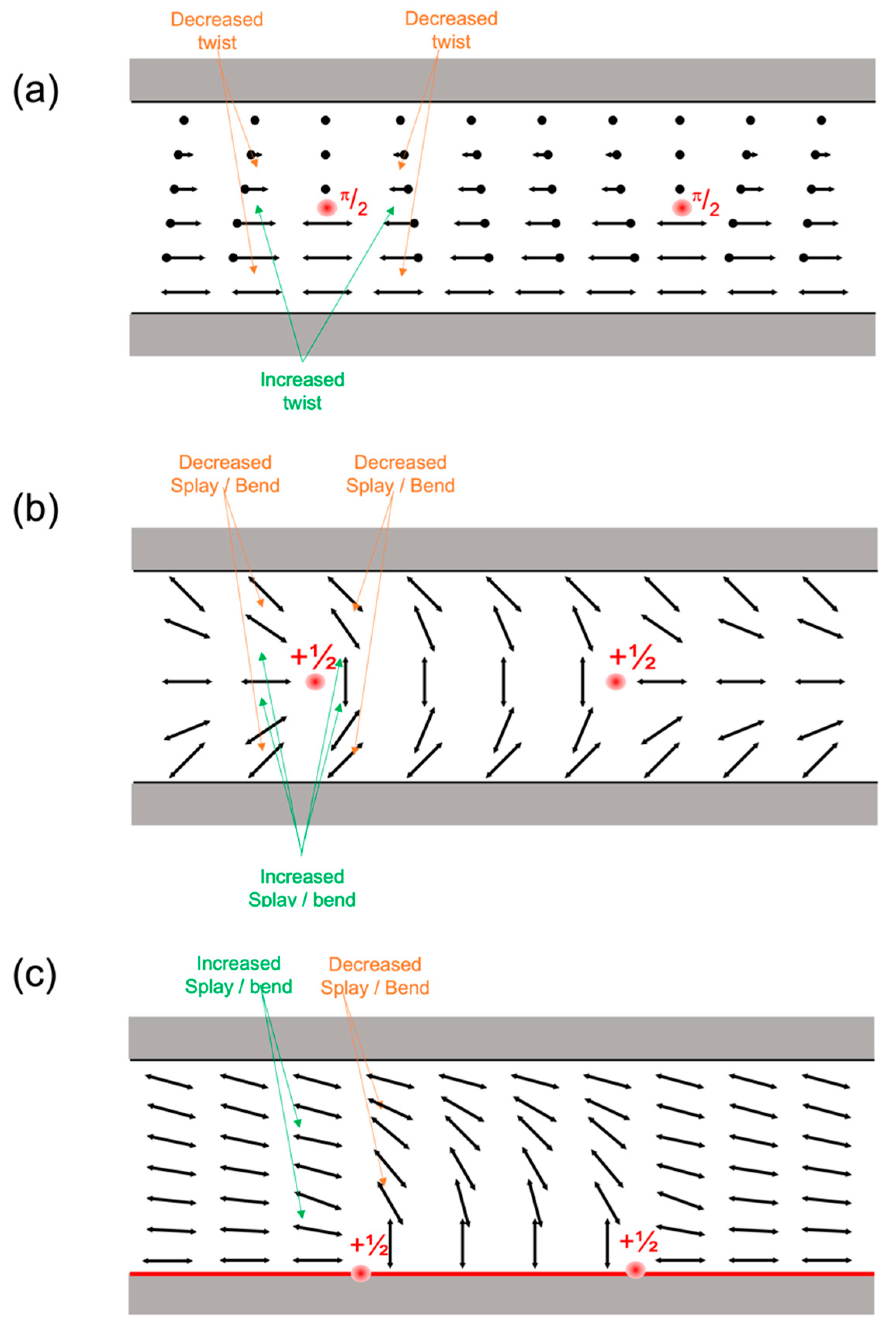
The application of liquid crystals in display, and other electro-optic and optical modulators, requires uniform alignment of the liquid crystal director in both the quiescent and switched states. Insufficient care in device design leads to unwanted defects between domains with different director profiles, causing scattering and unnecessary variations [
18]. For example, a 90° twisted nematic display potentially has topologically distinct director profiles with opposite senses of twist and tilt: either state cannot be transformed to the other without the formation of a defect wall [
18,
19], as illustrated schematically in
Figure 1a. Doping the nematic with a chiral material to give a preferred sense of twist, coupled with surface pretilts that favour that same sense of twist allows one sign of twist and splay/bend to form on removal of the applied field. Without these measures, the contrast ratio of a TN device would be too low and variable for display purposes due to scattering. Even so, unwanted defects can still form at pixel edges [
20], a factor that decreases the maximum resolution possible for nematic displays and spatial light modulators.
Rather than consider the defects as unwanted artefacts of poor device design, Bigelow and Kashnow [
19] considered the deliberate use of energetically equivalent but homotopically distinct twist states to form a bistable device. At that time, bistability showed substantial promise for highly multiplexed displays [
21] with more than a score of rows to be addressed because of the inherent non-linearity of the liquid crystal arrangement, and without the use of an additional semiconductor element such as a thin-film-transistor (TFT). In addition to showing the usual transient switching response to an applied electric field, bistable devices can also be latched between at least two optically distinct states. Latching occurs with some appropriate signal that provides sufficient impulse to overcome the activation energy that separates the bistable states. After the impulse, the new state is retained, and the device is said to be latched. Thus, an image is built up row by row; a scanning impulse is applied to the addressed row that is at, or near, the threshold value whilst a data signal of information is synchronously applied on the columns that either increases the impulse (latching) or decrease (non-latching, where the previous state is retained). In the work of [
19], surface inhomogeneities were used to pin the π/2 twist wall between states of opposing twist sense, and the states were selected electrically with fields applied using orthogonal interdigitated electrodes on the opposing surfaces. Although these initial attempts proved impractical, the use of topological defects to separate bistable states with different director profiles was a subject of much interest for several decades: the defect-mediated transition between states of different homotopy created a threshold voltage, and hence promised unlimited addressing without TFT. This drive stimulated attempts to use defects to induce vertical and horizontal bistable states in a nematic liquid crystal [
21,
22], such as those that form in parallel-aligned high pretilt nematic devices shown in
Figure 1b. Such devices were the first to show zenithal bistability, where the term zenithal refers to the out of plane angle that the director makes with respect to the device plane in the two bistable states. They did not receive any commercial development, due to the complexities of construction and latching mechanism. Following the successful commercialisation of low-cost TFT over large areas at high yield, the focus of bistable nematic display research moved to ultra-low power devices with image storage [
21].
ZBD is a commercially successful bistable nematic display invented in the UK [
4] and used in electronic shelf edge labels for the retail sector [
6,
7]. The technology has recently been acquired by New Vision Displays Ltd. [
23], and it continues to operate from its Malvern laboratories in the UK. Unlike the earlier zenithal bistable devices that relied on containment from the two opposing surfaces, the ZBD uses a single zenithally bistable surface, where the alignment surface itself has two different but stable pretilt states.
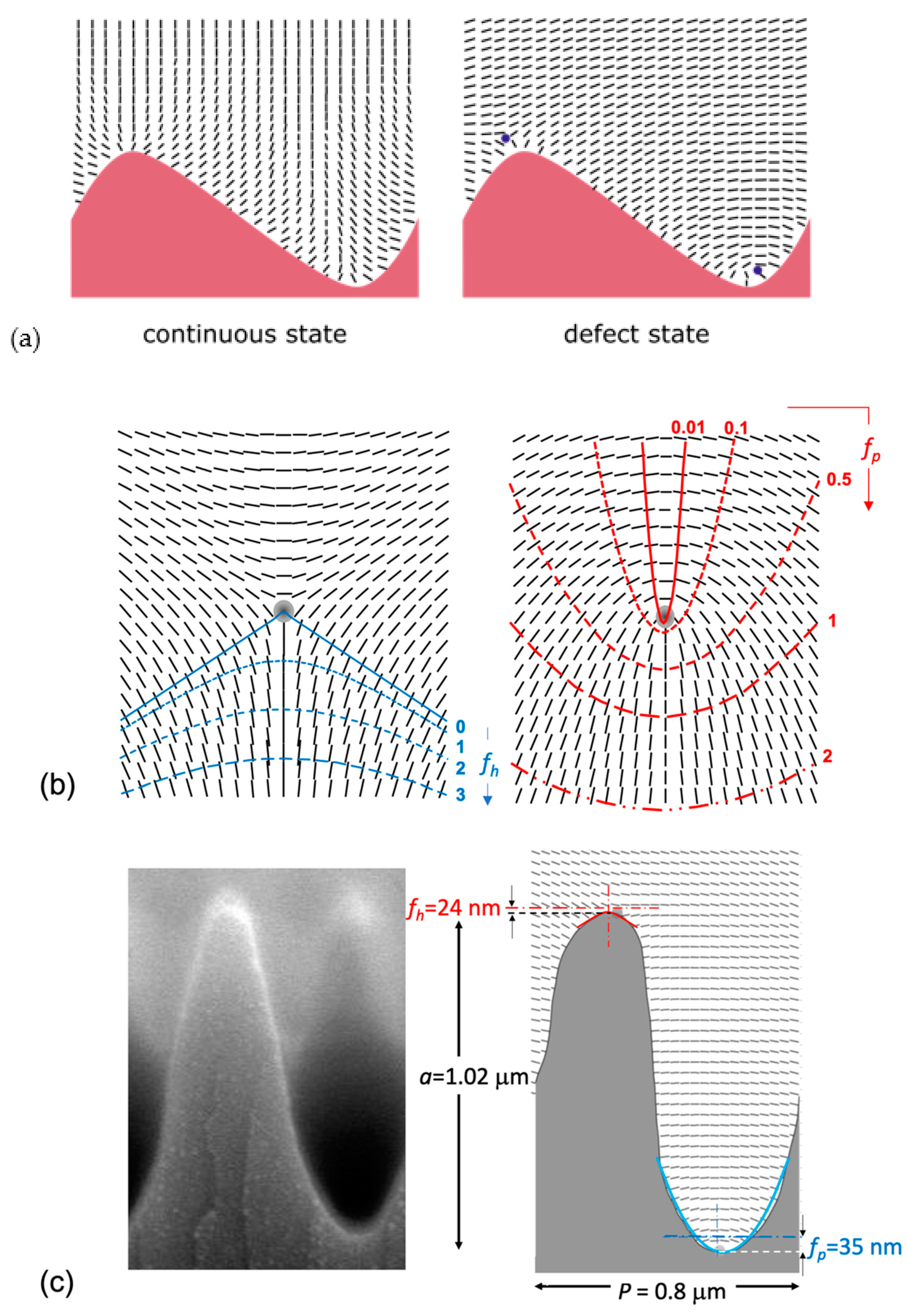
Figure 1c shows an example arrangement where a bistable surface that is either planar or homeotropic creates surface defects at the boundary between the states. In ZBD, the zenithally bistable surface is provided by a (sub)optical homeotropic grating that can stabilise −½ strength defects at the grating ridges and +½ defects at the grating troughs. Arranging the grating pitch
P to be approximately equal to its amplitude
a (
a/
P ≈ 1.0 ± 0.3) leads to both a defect-free (continuous, C) state and a defect (or D) state being stable and separated by an activation energy typically of the order 10
−5 J/m
2. An example of the grating used in a commercial device [
23] is shown in
Figure 2, wherein
a/
P ≈ 1.3.
Close to a homeotropic grating surface with sufficiently strong anchoring, an elastic distortion of the director field is induced if that field is to be continuous. In this continuous C state, the distortion dies down after a few hundred nanometres from the grating peaks, and the director is uniformly normal to the plane of the grating. Alternatively, the elastic distortion can be reduced by inducing the half-strength defects stabilised by the surface curvature, leading to a uniform and low tilt at a small distance from the grating plane. Examples of the C and D states are shown for a typical grating in
Figure 2a. This grating surface may be placed opposite either a homeotropic or planar homogeneous surface aligned perpendicular to the grating vector to give vertical-aligned to hybrid aligned nematic (VAN/HAN) or hybrid aligned to 90° twisted nematic (HAN/TN) display modes, respectively [
24], or opposing a second zenithally bistable grating surface to give VAN/HAN/TN [
25].
2. Surface Stabilised Topological Defects
The director profiles surrounding half-strength defects are illustrated in
Figure 2a, where an elastically isotropic nematic (K
11 = K
33) confined to the plane of the paper is assumed. In actuality, the defects are not points but lines that run perpendicular to the plane shown. The core is approximately a 50 nm diameter cylinder with uniaxial symmetry for the local director around the −½ defect and with biaxial symmetry around the +½ defect. These defects form loops that terminate at the boundary between D and C regions. Away from the core, the
n-director of an elastically isotropic nematic is a simple parabola for the +½ defect and hyperbolic with three-fold symmetry for the −½ defect. For an infinitely bound homeotropic surface with negative parabolic local surface curvature, the +½ defect will be at centered at the focal point
fp, as illustrated in
Figure 2b and given by:
where
x and
y are the orthogonal spatial coordinates with
y parallel to the defect axis. Similarly, the three-fold hyperbolic −½ defect has a focus at
fh for a positive hyperbolic surface with locus
and the defect is centered at
fh. Thus, for infinitely bound homeotropic surfaces, the topological defects sit near to the surface at a distance that is related to the degree of surface curvature.
Figure 2c shows a typical grating that can give zenithal bistability, together with the Q-tensor modelling from reference [
26]. If the grating were to have infinite anchoring, the +½ and −½ defects would sit at 35 nm and 24 nm, respectively. In the model, zenithal anchoring of W
θ ≈ 2 × 10
−4 Jm
−2, which is realistic of actual devices [
27], and the defects then sit at the grating surface (as indicated by the grey spots in
Figure 2c. The relationship between surface curvature and anchoring energy plays a critical role in these devices, and as shown in the current work, can lead to unusual switching and latching mechanisms.
Conventional voltage-dependent switching of the dielectrically anisotropic nematic will occur. For example, for a positive Δε material, the bulk director will increase its tilt angle to lie (anti) parallel to the applied field. Although this can lead to unwanted latching to the continuous C state, it will only act in one direction and cannot be used to give discrimination between the high tilt C and low tilt D states. Instead, polar switching from the flexoelectric polarisation is utilised to latch between these bistable states, where the term latching is used to denote a switching impulse that is sufficiently high to overcome some threshold value and the new state be retained after removal of the impulse [
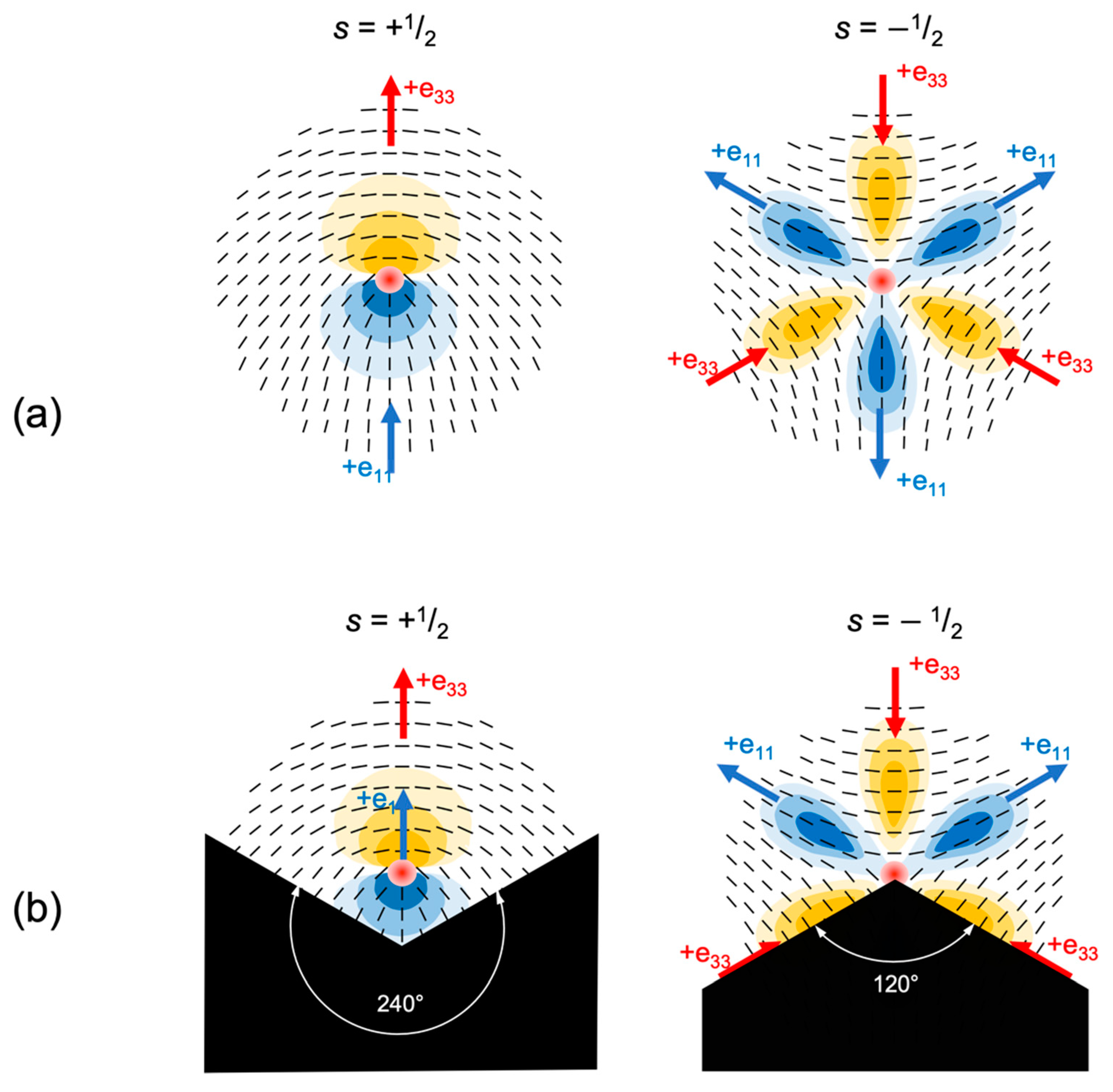
28]. In the ZBD, the elastic distortion is most strongly localised close to the topological defects, as illustrated in
Figure 3a [
29]. The sum of the flexoelectric components is small, being typically (e
11 + e
33) = 0.035 nC/m for the conventional twisted nematic mixture E7 [
30], and 0.2 nC/m for novel bent dimers specifically designed for flexoelectric applications [
31]. For comparison, a typical ferroelectric liquid crystal would have a spontaneous polarisation of 100 nC/cm
2. However, the elastic distortions in both the C and D states are concentrated to within ≈100 nm of the grating surface, from which we can estimate that the local polarisation is around 35–200 nC/cm
2 and the latching electro-optics of the ZBD is similar to that of an FLC (albeit with the slower optical response time associated with the much larger cell gaps used). This polarity may lead to forces and torques on the defects with an applied electric field. In the bulk liquid crystal, a −½ defect has three-fold symmetry and only a rotational electric torque, whereas the unipolar +½ defect has directionality and also undergoes a translational electric force [
32]. Thus, in the bulk of a nematic sample, electric field-induced movement of the defects is largely due to the +½ defects. However, these symmetries are broken when the defects are in proximity to a surface, as shown in
Figure 3b. Here, both defects have a net translational force that tends to move the defects along the surfaces to the points of maximum curvature, and then into the bulk of the device in the direction roughly parallel to the surface normal.
3. Conventional and Anomalous Latching between Bistable States
In practice, selective discrimination of either of the states is done using a bipolar electric pulse, wherein the polarity of the trailing pulse determines the final state. This helps ensure that there is no DC offset that may damage the liquid crystal compounds or lead to unwanted latching from the data applied to adjacent rows in a passive matrix addressing scheme [
28]. Moreover, the leading pulse of the opposite polarity to that of the latched state will elastically stress the director closer to the grating surface due to the switching effect of ε
0ΔεE
2. This in turn increases the flexoelectric polarisation and reduces the electrical impulse needed for latching [
28,
33]. When viewed on a microscopic level, the latching process occurs between an onset impulse (τV, where minimal domains of the new state are retained) to the fully latched state. The partial latching region is typically 1–2 V between the initial and full latch; this dictates the minimum data voltage required in the addressing schemes to give complete discrimination [
28].
Latching is a complex, three-dimensional process. The C-D transition involves nucleation of a defect pair at a discontinuity on the grating surface, usually deliberately defined using “slips” in the grating structure [
6,
7]. The defects form a loop that initially moves vertically across the grating surface to the apices of the structure, and then spreads in the direction of the grating peaks and troughs until joining with other loops on the same trajectory or another discontinuity. The full dynamics of this transition have not been simulated. Instead, literature studies [
26,
34,
35,
36,
37] use a two-dimensional Q-tensor model of the plane containing the normals to the device surfaces and the surface relief grating. Of these, reference [
26] is the only one that compares the predictions with experimental results. However, that work also shows that a simple, one-dimensional (1D) model proposed by Davidson and Mottram [
38] describes the behaviour adequately. That simple model uses a digital anchoring condition at the lower surface of
Figure 1c, wherein application of a torque sufficient to break the surface anchoring energy W
θ causes latching. The threshold pulse duration
and voltage
are related though [
26]:
where
is the rotational viscosity of the liquid crystal,
is the liquid slip length at the bistable surface,
is the cell gap adjusted to include the dielectric contribution of the grating,
is the flexoelectric sum,
is the applied voltage, and
is the threshold voltage:
is the vacuum permittivity,
is the dielectric anisotropy of the liquid crystal, and
is the bend elastic constant. Visualisation of fits is improved by rearranging Equation (3) to the linear form:
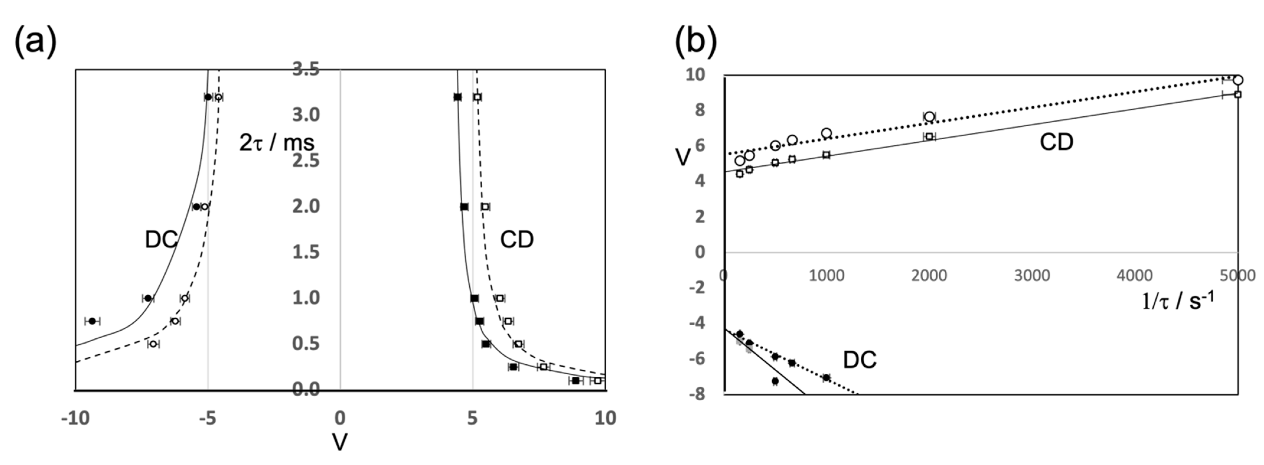
Figure 4 shows typical fits for the experimental latching thresholds for a ZBD test device to Equations (3)–(5) where the fitting parameters are given in
Table 1. All results in this work were taken using devices constructed by embossing an ITO-coated glass plate with a homeotropic photopolymer using proprietary grating film provided by Displaydata Ltd. The surface anchoring energy
was controlled through mixing of weak and strong photopolymers, also provided by Displaydata Ltd., as described in [
27]. The grating is spaced from a second ITO-coated glass plate, onto which the commercially available homeotropic polyimide SE1211 had been deposited, using 7 μm plastic spacer beads. This arrangement gives the VAN director profile for the C state and the HAN profile for the D state; when oriented with the grating at 45° to crossed polarisers, these states are dark and transmissive, respectively. Electrical waveforms were provided to the electrodes using an arbitrary waveform generator (WFG500 from FLC Electronics). Other than at short pulse widths, where unaccounted electrode losses begin to play a role, the simple (
V −
Vth)
−1 behaviour of the latching pulse width is evident in
Figure 4. It should be noted that
Vth is similar for both the C-D and D-C transitions, as expected. However, the large difference in A between the two transitions suggests different routes are taken by the defects in either case.
Various grating designs have been studied using this model, and the results were successfully compared with the experimental findings [
39,
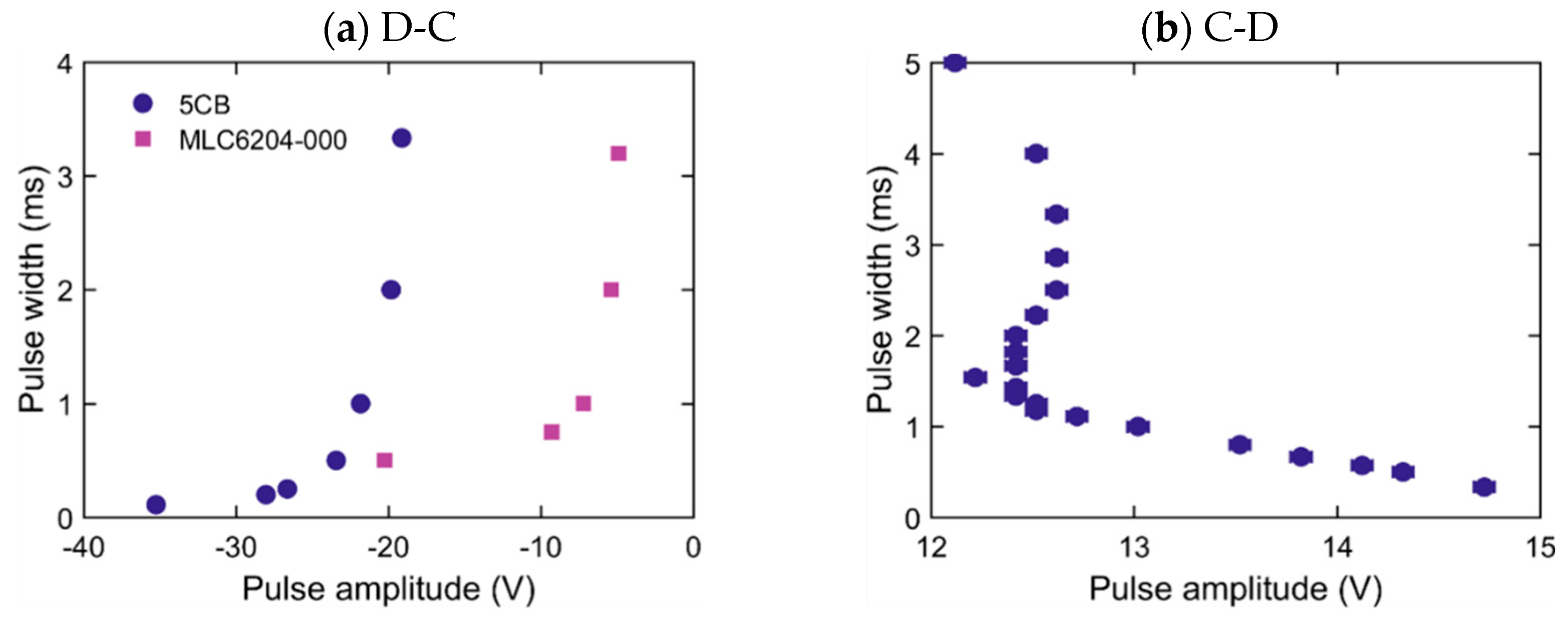
40]. However, in studying different liquid crystal materials and surface anchoring energies as part of this study, it was found that the form of the latching deviates occasionally from this expected behaviour. For example,
Figure 5b is the C to D latch curve for single compound pentyl-cyanobiphenyl (5CB) at 30 °C in a 7 μm cell constructed with a high anchoring strength photopolymer grating. Instead of diverging at a threshold voltage
Vth, latching at the longer times requires a higher voltage, not lower. This leads to degenerate behaviour at a particular voltage, wherein pulses of three different durations all lead to full latching.
Understanding the dynamics that leads to this behaviour required 2D finite element modelling, which is reviewed in the following sections.
4. Q-Tensor Modelling
A 2D finite element discretisation of the Landau-de Gennes free energy is performed to examine the dynamics of the device. A finite element solution to the Qian and Sheng formalism [
41] was found using the program
Q-LCSolver, as described in [
35,
36]. For a complete treatment of the software, the interested reader is referred to [
37], but a simple review of the approach is included below. Although the program solved in 3D, the third (y-) dimension was disregarded for most of the simulations, to save computational time and a 2D model used. Time saving measures were particularly important to find the latching thresholds and defect dynamics both above and below the threshold. Sub-microsecond time steps were used to allow for the defect dynamics, but applied over sufficient time following the applied fields to allow the bulk director reorientation to complete (usually tens of milliseconds). Moreover, many simulations of both time and voltage are done for each point plotted to allow the onset and completion of latching to be calculated. It should be noted that the model has previously been used to investigate the behaviour of defect loops [
42], and in particular the path of the defects at phase shifts deliberately added to the grating structure in commercial devices [
6]. For the qualitative description of the current work, the 2D model was found to be sufficient.
The program uses the Q-tensor representation for liquid crystals, which accounts for the head–tail symmetry of the nematic director and changes to the order parameter, such as those that occur close to defects and surfaces. In the uniaxial case, this is written:
where
i and
j are integers from 1 to 3,
S is the scalar order parameter,
n is the director, and
is the Kronecker delta. The total free energy
Ftot of the system in a device of volume
with surfaces
is taken as:
This equation includes the thermotropic bulk free energy density
, the elastic distortion energy density
, the electric energy density
, and the surface elastic energy contribution
. The thermotropic energy density is written as:
and the Landau de Gennes critical coefficients
and
were taken from [
26]. Elastic distortion energy density takes the form:
where
and
are constants related to the Frank elastic constants
,
, and
and the splay-bend and chiral terms have been omitted.
The electrical free energy density includes the flexoelectric term:
Here, the flexoelectric polarisation vector
P can be written in terms of the director as:
with
e11 and
e33 representing the flexoelectric coefficients for splay and bend deformations of the director, respectively. In the limit of constant uniaxial order parameter, the polarisation can be written in terms of the
Q tensor [
43]:
The relative dielectric tensor
in Equation (11) is:
where
is the dielectric anisotropy of the liquid crystal material and
S0 is the equilibrium scalar order parameter (approximately
S0 ≈ 0.6 in this instance). The electric field was found from the potential
, which satisfies the Poisson equation:
where the charge density
is considered solely due to the flexoelectric polarisation,
from Equation (11). For the surface aspect of the free energy, the model includes the possibility of weak anchoring at the cell walls. In this case, the surface elastic energy contribution takes the form:
where
and
are orthogonal unit vectors perpendicular to the alignment direction. Anchoring is then controlled through three parameters:
and the anchoring strengths
and
, which are associated with the surface tilt and twist deformations.
The dynamic behaviour of
is determined by the frictional losses in a Raleigh dissipation equation:
following the approach of [
44], where
δ represents infinitesimal changes in the power
and the frictional losses
D. Equation (16) represents a conservation condition where changes in total energy are balanced by the dissipation effects. The dissipation function
D is a function of
and the flow velocity of the liquid crystal and represents the dissipation effects due to rotational and translational flow [
37]. In the current work, the effects of flow were not included and only the rotational viscosity γ
1 used.
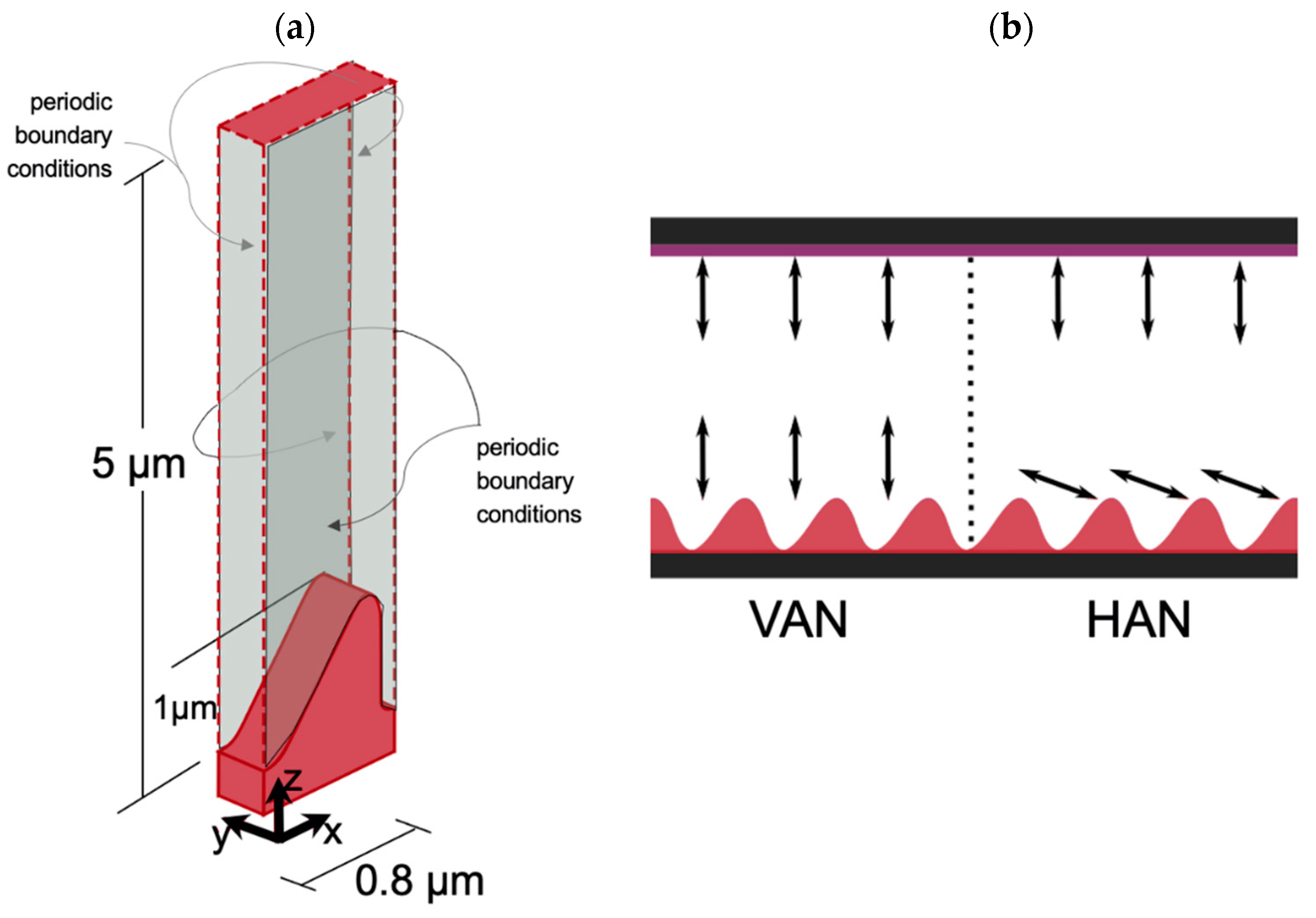
The modelling volume is that of a single pitch of the grating surface at the base of a 5 μm device,
Figure 6. It is assumed to be infinitely repeating through periodic boundaries in x and y where a 1 μm depth is modelled in the y direction. Both the top surface (in z) and the grating surface are given homeotropic boundary conditions, thereby matching the configuration of the experimental cells. The top surface anchoring is assumed infinite, whereas the grating surface anchoring was varied between weak 5.0 × 10
−5 J/m
2 and strong 2.8 × 10
−4 J/m
2, as determined in [
27]. Note, the term strong is often used to mean infinite anchoring in the prior literature, whereas here it denotes a relative magnitude. Unlike [
26], which used the spline of the grating surface from an experimental SEM of the commercial device shown in
Figure 2c, a simple but representative blazed sinusoidal surface was used with an 800 nm pitch and 1.0 μm amplitude. The blaze was high enough to induce pretilts of 25° and 89.5° in the D and C states, respectively. These were sufficient to prevent any degeneracy induced by the fixed top surface. To save on computational time, an adaptive mesh was used, wherein the initial density of mesh points was high close to the grating surface. Results of the simulations were analysed in two dimensions using slices of the x-z plane. The simulations were set to output data on every tenth iteration, giving a clear view of the defect behaviour while reducing data handling. Results were evaluated in the data analysis and visualisation program
ParaView. The surface slip values were estimated by a linear extrapolation of the near surface director over several frames using
ImageJ, with an error calculated according to the variation found at different parts of the surface.
Liquid crystal parameters were chosen to coincide with that of previous modelling [
26] and measurements [
39] and are listed in
Table 2. Although the parameters have not all been determined for the commercial nematic mixture MLC6204-000, but rather a bespoke formulation made to give low voltage and fast flexoelectric latching (mixture B from [
45]), they are expected to be typical of the highly positive Δε nematics used in commercial devices. This enables a qualitative study at least of the latching behaviour and the corresponding defect dynamics.
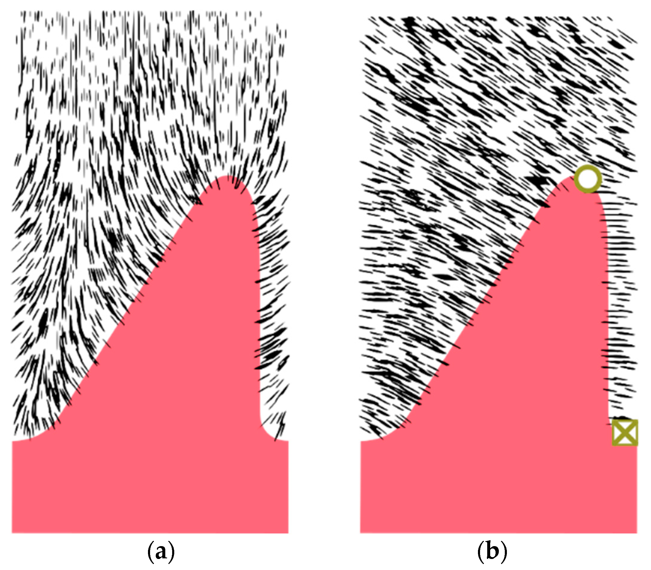
For each anchoring energy, the two equilibrium profiles were first found for the continuous and defect states. For the C state, the director was initially set to vertical throughout the bulk of the cell and allowed to reorient over 5 ms. An analogous process was used for the D state, allocating a horizontal planar bulk orientation, and allowing 50 ms for the reorientation. This required a longer time due to the hybrid alignment of the D state and the elastic distortion throughout the bulk of the device. The resulting director profiles for a given anchoring condition were used as the starting conditions for the subsequent runs. For example,
Figure 7 shows the resultant quiescent director profiles for the W
θ = 2.8 × 10
−4 J/m
2.
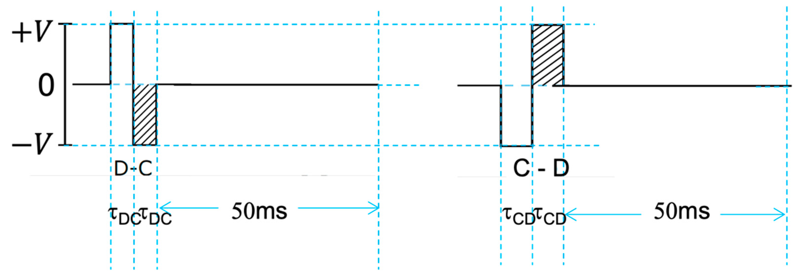
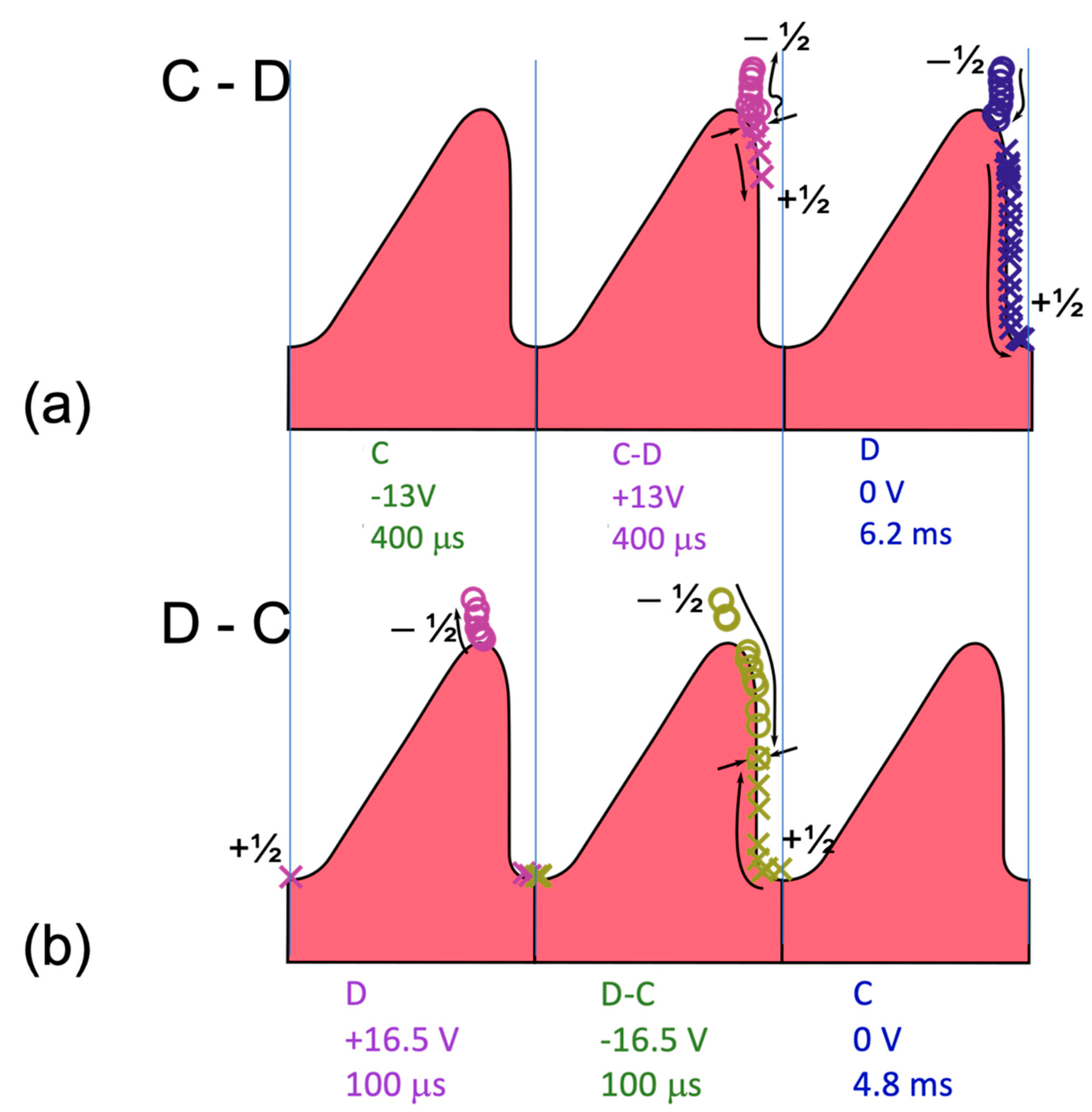
Electrically induced latching between the states was studied for bipolar pulses of the form shown in
Figure 8. The polarity of the trailing pulse determines the selected state, with the trailing pulse being positive on the grating surface tending to give the D state. For instance, to latch from continuous to defect state, first a negative pulse is applied, followed by a positive pulse of equal magnitude, followed by a period of between 10 ms and 20 ms with no field applied, to allow the bulk director profile to relax to its final state. For each voltage and time, the final state is determined, and the process repeated for a new impulse
until the change of state is found. Latching may be either successful or unsuccessful, depending on the impulse of the trailing pulse. For a given time, the threshold pulse height is then recorded as the midpoint between the highest-voltage unsuccessful latch and the lowest-voltage successful latch. The error bars are then set as the width between those two values.
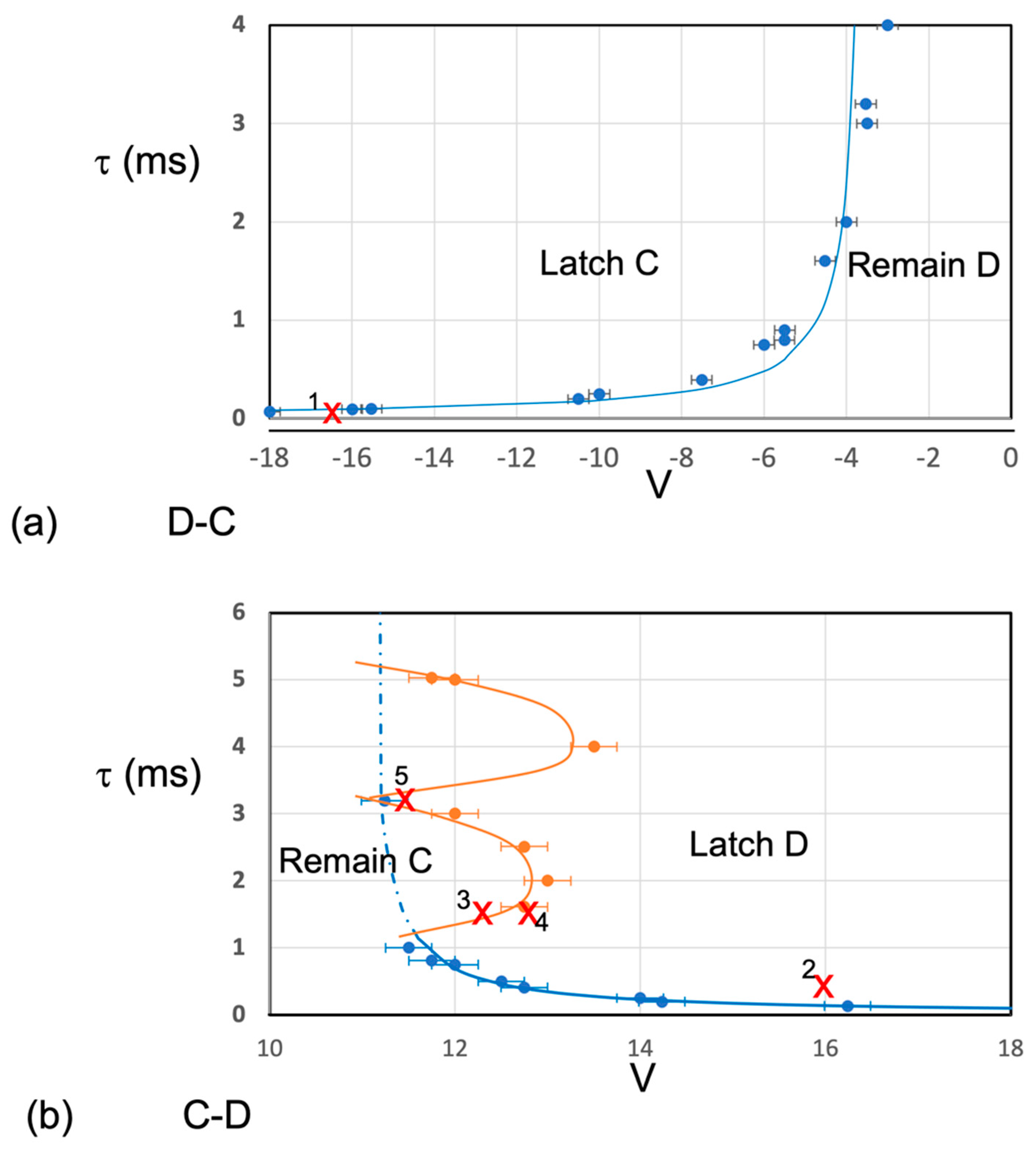
5. Simulations of Anomalous Bistable Latching
Latching from C-D and D-C was investigated for anchoring energies ranging from 1 × 10⁻⁵ N/m ≤ Wθ ≤ 2.8 × 10⁻⁴ N/m. For anchoring at and below 5 × 10⁻⁵ N/m, the continuous state did not stabilise, and the device was monostable. The defects were submerged into the surface and the director profile was uniformly at the 25° pretilt defined by the grating blaze. Experimental observations agree that the bistable states are lost for weak anchoring of this magnitude. However, unlike the 2D simulation, the director orients into the xy plane to have a higher component parallel to the grooves. That is, when the defects are significantly below the surface, the director tends towards the continuous state for a planar-aligned grating. However, it is instructive to note that the failure to give the D state in the 2D simulation occurs at a similar anchoring strength to that found experimentally, which adds some confidence to the validity of the model and (static) parameters used.
The τV characteristics were modelled for a d = 5 μm ZBD using the liquid crystal properties of
Table 2, for weak (W
θ = 1.0 × 10
−4 N/m) and strong (W
θ = 2.8 × 10
−4 N/m) anchoring conditions. The results are summarised in
Table 3, and the full characteristics for the strong anchoring case shown in
Figure 9.
Table 3 includes the fits of the simulated data to Equation (5), using the surface slips found in the simulations. For the weak anchoring, the reciprocal behaviour was followed for both D-C and C-D transitions across the whole range, but the quality of fit to the form of Equation (5) was poor. For example, the threshold voltages from the fits were consistently higher than that indicated by the low voltage latching. Moreover, inputting the liquid crystal parameters used for the simulations into Equations (3) and (4) also gave substantial differences. The simulated behaviour of the CD latching characteristic for the strong anchoring deviated from the reciprocal form of Equation (5) quite dramatically, as evident in
Figure 9b. Here, the reciprocal fit was satisfactory for short pulse widths and high voltages, but at lower voltages, the threshold swapped to higher voltages than expected. This type of behaviour is reminiscent of the anomalous latching seen in some experimental results, such as those shown in
Figure 5. Hence, we investigate the latching mechanisms in more detail, in particular the defects trajectories during the switching process at five points shown in
Figure 9: two of conventional latching behaviour (1 and 2) and three in the region of anomalous C-D latching (3, 4, and 5).
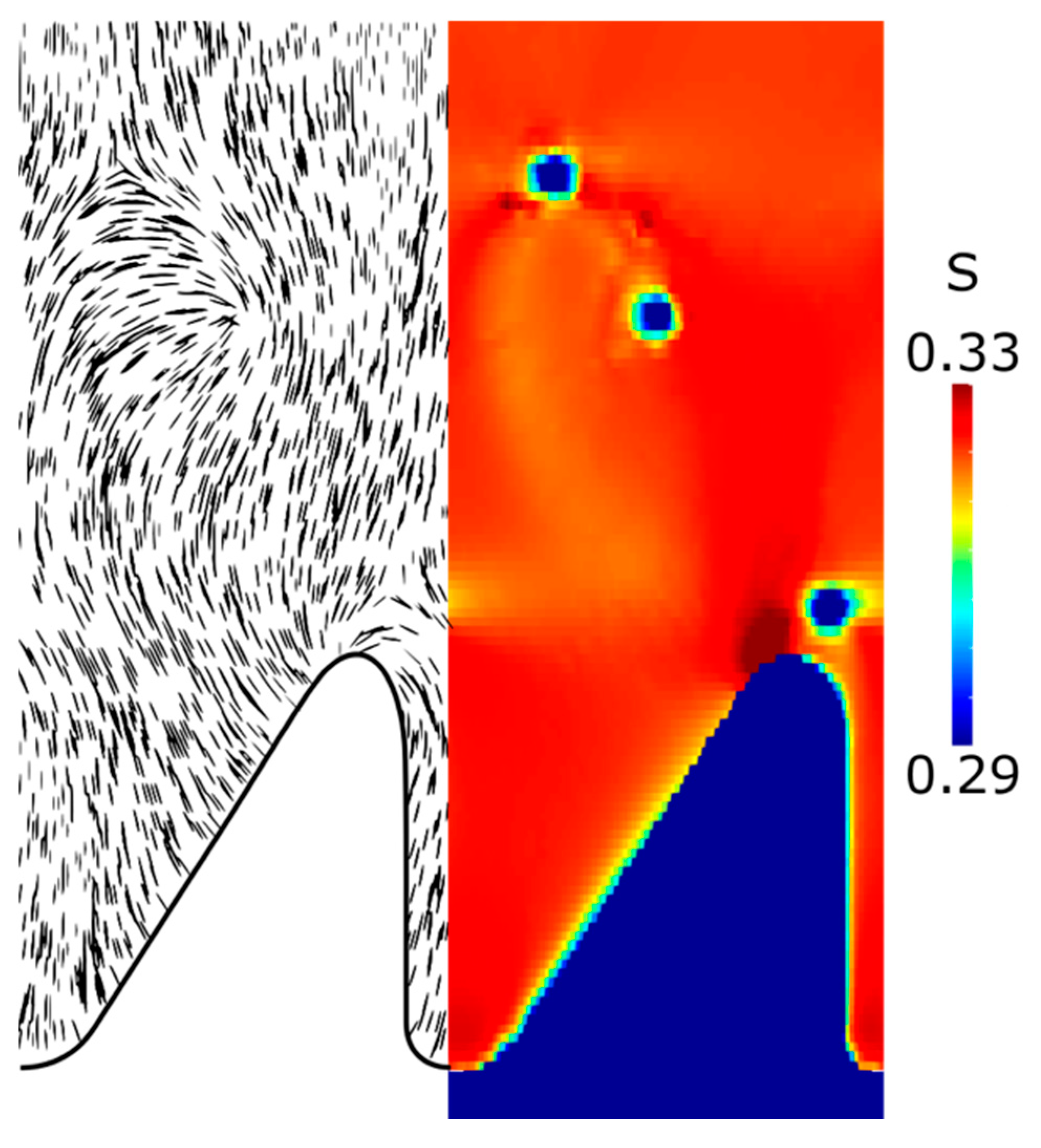
Figure 10 shows the typical trajectory of the defects when undergoing normal latching. For these and the subsequent figures, only the near-grating regions are shown; the director profile extends for a further 3 μm or so to the top surface. Where the order parameter S is shown, variations in the range 0.2 to 0.4 are emphasised, to allow visualization of the defect and surface distortion regions. For all cases, the liquid crystal undergoes the normal ε
0ΔεE
2 response in the bulk of the liquid crystal when the electric field is applied.
Since the material is strongly positive (Δε = +39), the bulk director reorients towards the vertical condition regardless of whether the initial state is C or D, and the response time is expected to be between 1 ms (for ±4 V) and 0.2 ms (for 10 V). This RMS response serves to both increase the local flexoelectric terms close to the surface, and to reorient the director away from the grating more towards the vertical condition.
The D-C simulation shown in
Figure 10b and in
Video S1 corresponds the conditions given by point 1 in
Figure 9. The leading (positive) pulse pulls the −½ defect away from the grating peak to some distance within the bulk of the cell that depends on the impulse
. This initial field has minimal effect on the +½ defect lying in the trough of the grating groove. This is consistent for all results, wherein the +½ defect moves towards the positive electrode and the +½ defect towards the negative electrode. On reversal of the field the trailing (negative) latching pulse propels this +½ defect up the grating sidewall, whilst the −½ defect returns to the grating surface and moved down the surface to meet it. The two defects annihilate, either during the latch pulse or, if within critical proximity, during the subsequent reorientation time. Should the voltage be insufficient for latching, the defects will resettle at their original positions on the grating following the reverse trajectories on the side walls of the grating.
The initial response, where the −½ defect moves into the bulk due to the leading pulse means that the trajectory for annihilation in the trailing pulse is lengthened. This is likely a cause for the breakdown of the simple 1D model and poor fits from Equation (5) since the resulting increase in latching time will be directly related to the magnitude of the field. Indeed, at low voltages (≤|10 V|), the −½ defects do not leave the surface at all during the positive pulses. In this regime, the +½ defects also remain quite static at the bottom of the groove during the trailing negative pulse of the D-C latching sequence.
Similarly, the defect trajectories for C-D latching at point 2 of
Figure 9 are shown in
Figure 10b and
Video S2. During the first (positive) pulse, no defects are observed; refraction of the electric field caused by the grating will cause a divergence at the point of inflexion on the side walls, but defects are prevented from forming by the surface curvature. Once the field is reversed in the trailing pulse, the field causes the nucleated defects to separate and move in the directions where the grating curvature stabilises each defect. In the instance shown, the +½ defect only moves part of the way towards the grating groove, but the −½ defect passes the top of the grating and begins to move into the bulk. On removal of the field, the +½ defect travels down the sidewall to the base of the groove and the −½ defect returns to the grating peak. Note, in this instance the D state forms during the relaxation process after the pulses have ended. If the pulse impulse is too small then either no defect nucleation occurs during the positive pulse or there is insufficient separation of the defects at the pulse end, leading to mutual annihilation; neither instance leads to latching.
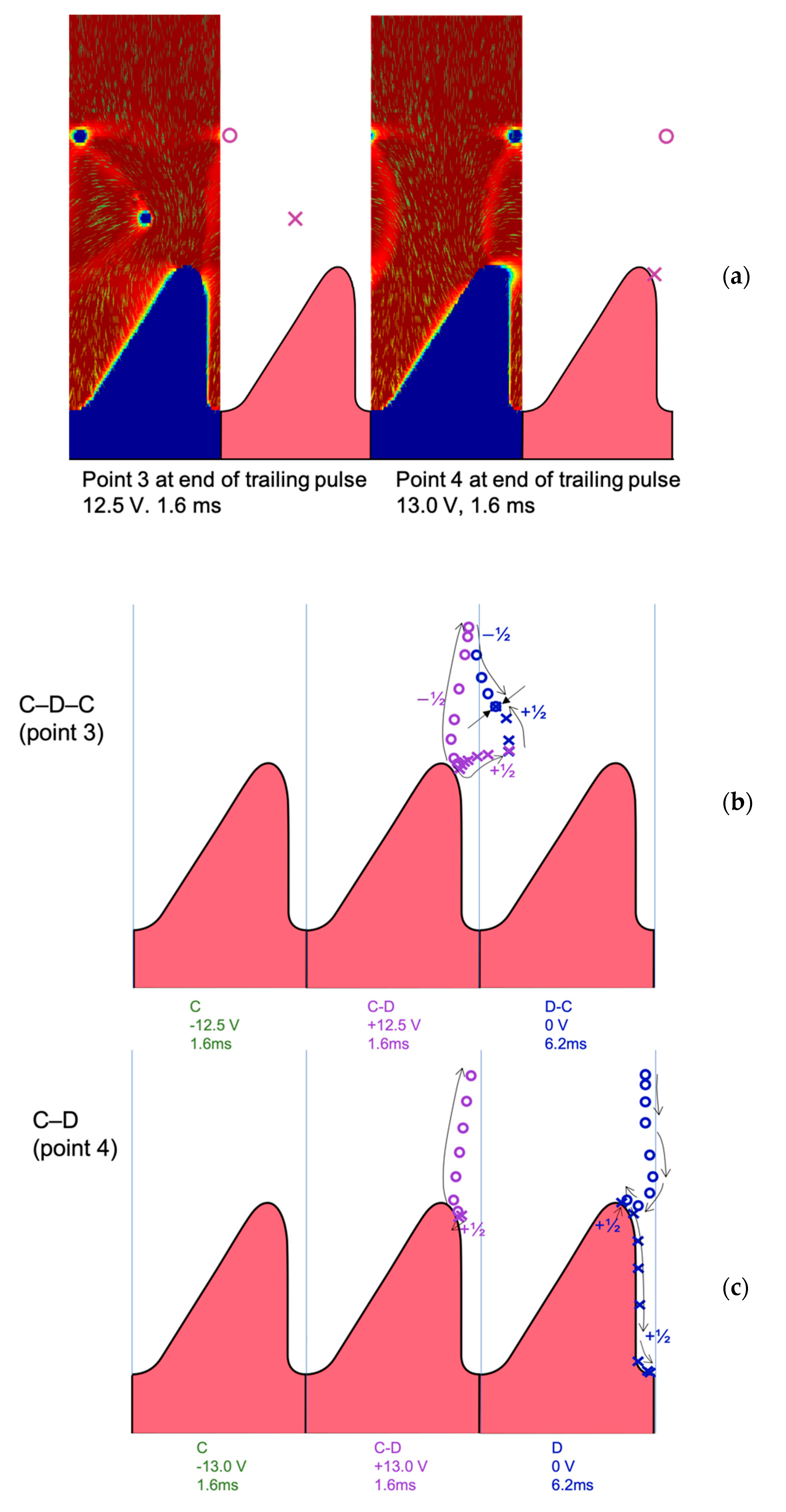
The impulses at points 3 and 4 in
Figure 9b are immediately below and above the latching threshold, respectively, in the range where the latching is anomalous and requires a significantly higher impulse than that expected from the reciprocal relationship of Equation (5).
Figure 11 shows the position of the two defects at the end of the trailing pulse for both point 3 and point 4, together with the corresponding defect trajectories (also given in
Video S3. The −½ defect follows similar trajectories in either case, moving from the initial nucleation point on the grating to deep within the bulk of the cell at the end of the pulse sequence. However, the +½ defect shows considerable differences in behaviour. For the lower voltage of point 3, the +½ defect detaches from the surface and enters the space between the grating grooves. After the pulse, the two opposing defects in the bulk of the liquid crystal move to mutually annihilate and the director profile relaxes to the C- state. Thus, despite a large impulse with the correct sign of trailing pulse to latch to the D state, latching does not occur and the C state is retained. Raising the voltage slightly to 13.0 V (point 4) then prevents the +½ defect from detaching from the surface and its movement is suppressed until the field is removed, when it again slides down the grating towards the groove where it remains, and the D state is latched.
The cause of such a dramatic change in behaviour is due to differences in the local director profile and defect orientations at the start of the trailing pulse. Reference [
32] has shown quite substantial differences in defect trajectories on their paths to spontaneous annihilation due to their relative starting orientations. In particular, the +½ defect follows a path parallel to the local director. In this work, the situation is further complicated by the effect of the surface, the electric field, and its refraction. At the lower voltage, the director has reoriented less in the bulk of the sample and forms a path into the space between the grooves into which the +½ defect can move. With the higher field, the director is vertical closer to the defect, and the +½ defect movement into the bulk is impeded. As described in
Section 1, defects on a strongly anchored surface will sit slightly further into the bulk than for weakly anchored, thereby are more likely to detach from the surface and move into the bulk of the liquid crystal.
Latching at point 5 in
Figure 9 was also studied, as shown in
Figure 12 and
Video S4. Here, the 3.2 ms pulse is sufficiently long that the two defects move far into the bulk during the trailing (positive) pulse application. The director distortion around the grating surface also increases and supports the nucleation of a second pair of defects. As the original pair annihilate each other, this second generation behaves in the same fashion as the defects for shorter pulse widths, and thus are similar to the conventional latching mechanism. For voltages higher than the latching threshold at point 5, eventually this second-generation defect pair will enter the bulk together as the first pair did, which suppresses latching once more. Similarly, with even longer pulse widths, such as the data at 5 ms pulse widths in
Figure 9, the second-generation pair also annihilates in the bulk. With successively longer pulse widths we see further generations of defects created in much the same way.
The simulation times for pulses longer than 5 ms were excessive, for which the maximum number of defect pairs was third generation (indicated by the upper orange loop in
Figure 9b). However, up to seven generation have been found for very high anchoring energies of W
θ = 5 × 10
−4 N/m. The formation of higher-generation defects may also occur above the latching threshold, for the short pulse widths. It is clear from
Figure 11 that the defects at point 5 are injected into the bulk of the cell and remain there until the field is removed, when they relax to the respective low energy states at the regions of highest surface curvature. However, at voltages above the threshold, further defect pairs can be formed at the top of the grating and propelled into the bulk. When the field is removed, the defects closest to the grating follow a similar path to those shown for point 4 in
Figure 11, whereas the earlier defects move towards each other and mutually annihilate following similar paths as that of point 5 in
Figure 11.
This behaviour of multiple defect pairs being propelled into the bulk of the sample will be strongly related to grating shape. For example, the gratings studied in reference [
26] were more symmetrical and with less blaze than that used in the simulations here (see
Figure 2c). In that case, further defect pairs were detected that were nucleated on the opposing sidewall of the grating, whereas here the multiple defect generation is being nucleated from the same point. It should also be recognised that, in the experimental studies of reference [
45], reverse latching occurred at impulses above those for latching. That is, a negative-positive train would latch to D but increasing the voltage beyond a second threshold led to latching back to the C state. This transition was ascribed to the ionic content in the mixtures, causing a similar reverse latching to that in ferroelectric liquid crystals [
46]. In this instance, ions diffuse to reduce the applied DC field, creating a reverse field. After the field is removed, the reverse field is retained briefly and before the ions have time to redistribute, which can be sufficient to cause latching from the desired state back to the opposite state. Instead of this explanation, it is possible that reverse latching might be due to forcing the defect pairs into the bulk where they annihilate (as found in this work). However, this would apply to C-D latching only, whereas reverse latching was observed for both C-D and D-C latching. Hence, the ionic viewpoint remains more likely because and was removed using commercially pure STN materials with typical room temperature conductivities of 10
−11 Ω
−1 cm
−11 to reduce the ionic content [
45]. However, the current work suggests that various types of behaviour are possible when including both multiple defects and ionic effects.


