
The Transition from Type-I to Type-II SiC/GaN Heterostructure with External Strain

1
School of Electrical Engineering, Anhui Technical College of Mechanical and Electrical Engineering, Wuhu 241000, China
2
School of Information Science and Technology, Nanjing Forestry University, Nanjing 210037, China
3
School of Mechanical Engineering, Southeast University, Nanjing 211189, China
4
Automotive & Transportation Engineering, Shenzhen Polytechnic, Shenzhen 518055, China
5
Wenzhou Institute, University of Chinese Academy of Sciences, Wenzhou 325000, China
6
Dean’s Office, Xuancheng Vocational & Technical College, Xuancheng 242000, China
*
Authors to whom correspondence should be addressed.
Crystals 2024, 14(1), 30; https://0-doi-org.brum.beds.ac.uk/10.3390/cryst14010030
Submission received: 12 November 2023
/
Revised: 5 December 2023
/
Accepted: 8 December 2023
/
Published: 27 December 2023
(This article belongs to the Special Issue Wide Bandgap Semiconductor: GaN and SiC Material and Device)
Abstract
:Two-dimensional materials are widely used as a new generation of functional materials for photovoltaic, photocatalyst, and nano-power devices. Strain engineering is a popular method to tune the properties of two-dimensional materials so that performances can be improved or more applications can be obtained. In this work, a two-dimensional heterostructure is constructed from SiC and GaN monolayers. Using first-principle calculations, the SiC/GaN heterostructure is stacked by a van der Waals interaction, acting as a semiconductor with an indirect bandgap of 3.331 eV. Importantly, the SiC/GaN heterostructure possesses a type-II band structure. Thus, the photogenerated electron and hole can be separated in the heterostructure as a potential photocatalyst for water splitting. Then, the external biaxial strain can decrease the bandgap of the SiC/GaN heterostructure. From pressure to tension, the SiC/GaN heterostructure realizes a transformation from a type-II to a type-I semiconductor. The strained SiC/GaN heterostructure also shows suitable band alignment to promote the redox of water splitting at pH 0 and 7. Moreover, the enhanced light-absorption properties further explain the SiC/GaN heterostructure’s potential as a photocatalyst and for nanoelectronics.
1. Introduction
Graphene has been obtained successfully using the micromechanical stripping method and explored for promising advanced applications because of its unique Dirac cone [1,2]. For example, graphene exhibits fascinating carrier mobility up to 15,000 cm2V−1s−1 at room temperature [3], which can be used for electronics and sensors [4,5]. Moreover, remarkable optical transparency was developed for optoelectronics [6]. However, the gapless nature of graphene limits its usage in field-effect transistors [7], and its excellent thermal conductivity (about 0.4 × 10⁴ Wm−1K−1) [8] implies that graphene is not suitable for thermoelectronics [9]. The TiSi2N4 monolayer presents an ultrahigh electron mobility of about 1.04 × 104 cm2V−1 s−1 [10]. In particular, Janus TMDs have attracted much attention in recent years due to their intrinsic built-in electric field, which is due to the asymmetry of the out-of-plane structure [11]. A two-dimensional (2D) material refers to a material with a thickness of only a single atom or several atomic layers [12,13,14,15]. For example, phosphorene is a direct bandgap semiconductor and has a honeycomb structure, which makes phosphorene act as an excellent 2D material suitable for various applications, such as field-effect transistors, flexible micro/nanodevices, spintronics, solar cells, biomedicine applications, and photocatalysts. This material has unique electrical [10,16,17,18], optical [19], mechanical [20,21,22], and thermal properties [23,24,25]. However, some measures need to be taken to break through it, giving it further special properties and expanding its application. Therefore, it has broad application prospects in electronics and optoelectronics. The discovery of graphene has sparked research into other 2D materials, including materials such as MoS2 and AlN. In recent years, researchers have also discovered some new 2D materials, such as transition metal dichalcogenides (TMDs), phosphorene, and arsenene. These materials have different properties and applications and can be used to prepare new electronic components, sensors, and energy-storage materials [26,27]. At the same time, there are many methods for preparing 2D materials, including mechanical stripping, chemical vapor deposition, solution stripping, and so on. The development of these methods has made the preparation of 2D materials simpler and more controllable. In addition to applications in fields such as electronics and optoelectronics, 2D materials also have broad application prospects. For example, molybdenum disulfide (MoS2) is a direct bandgap semiconductor with a bandgap of 1.8 eV. It has excellent tribological properties and can be used to prepare friction materials [28]. PtS2 possesses a high absorption rate in the visible light range, making it widely applicable in the field of optoelectronics [29,30]. With the continuous development of preparation methods and in-depth research, it is believed that more novel 2D materials will be discovered and applied to various fields.
Energy-storage methods have been extensively studied [31,32]. It is cutting-edge to use 2D materials as functional materials for energy storage or energy conversion [33]. For 2D materials, the most common and effective way to change their physicochemical properties is with metal impurity doping, especially by changing their conductivity and magnetism. For instance, graphene can be doped with platinum-group elements (ruthenium, rhodium, palladium, osmium, iridium, and platinum). Using density functional theory (DFT) calculation, it can be found that the structural, optical, and electronic properties of graphene are enhanced [34]. To further develop the performance of these 2D materials, the usual approach is to synthesize new materials by stacking and assembling them into a heterostructure. These layered materials are held together with van der Waals forces [35]. For these van der Waals heterostructures, due to the differences in lattice constants, lattice structures, and band structures of different materials, the behavior of electrons near the heterostructure may differ from that of a single material, resulting in a series of unexpected electrical and optical properties [36,37,38]. The formation of the heterostructure can be achieved using various means, such as chemical vapor deposition, physical vapor deposition, molecular beam epitaxy, metal–organic chemical vapor deposition, etc. Meanwhile, due to the different band structures between the two materials, there may be band-bending and band-offset phenomena [39,40,41]. In most current studies, the two most common types of heterostructures appear, namely, type-I and type-II heterostructures. The type-I band structure refers to a heterostructure with the conduction-band minimum and the valence-band maximum in the same layer. The main characteristic of a type-I heterostructure is the separation effect of electrons and holes, which enables the material to have higher electron mobility and better carrier transport performance. In addition, due to the formation of electric potential barriers at the heterostructure interface, this structure can also achieve the effective separation of electrons and holes, therefore improving the efficiency of the device. For example, the average carrier of type-I heterostructure materials constructed using PbI2 and WS2 is 0.039 cm2·s−1. It can be observed that the interlayer diffusion behavior between electrons and holes is similar [42]. MoS2 and ReS2 were constructed into type-I heterostructure with van der Waals forces, and it was found that when carriers were injected into ReS2, the carrier lifetime in the heterostructure was similar to that of single-layer ReS2, further demonstrating the lack of charge separation [43]. In summary, the type-I heterostructure is an important structure in semiconductor devices, which has the separation effect of electrons and holes and efficient carrier transport performance. The type-II band structure means the conduction-band minimum and the valence-band maximum are induced by different layers so that the photogenerated charges can be prevented from being recombined. Many 2D heterostructures are calculated to be formed by van der Waals forces as a photocatalyst for water splitting, such as phosphorene/BSe [44], MoSe2/Ti2CO2 [45], and TMDs/BP [46]. A WS2/CeO2 heterostructure was prepared using an ultrasonically assisted method, which possessed a covalent bonding interface. The WS2/CeO2 heterostructure presents the type-II band structure with an excellent photocatalytic activity of about 446.7 µmolg−1 CO2 generation [47]. Recently, monolayer Honeycomb SiC was successfully prepared using the bottom-up growth method [48]. The 2D SiC also presets novel electronic [49] and mechanical [21] properties. Furthermore, GaN also shows stability [50] and is successfully synthesized in experiments [51]. The excellent mechanical properties of GaN were obtained [20], showing particular stress characteristics as a heterostructure with SiC. The van der Waals heterostructure based on GaN or SiC monolayers was also reported, such as MXene/GaN [52], MoSSe/GaN [53], blue phosphorus/SiC [49], SiC/TMDs [54], suggesting use as photocatalytic, photovoltaic, and optical devices. More importantly, the heterostructure formed by GaN and SiC monolayers presents a small lattice mismatch, which means it an easier to prepare in experiments.
In this investigation, SiC and GaN monolayers are selected to construct a heterostructure. The most stable stacking structure of the SiC/GaN heterostructure is obtained, and ab initio molecular dynamics (AIMD) simulations are used to further prove thermal stability. Using first-principle calculations, the electronic and optical performances are calculated. Importantly, the SiC/GaN heterostructure can complete the switching from a type-II to a type-I semiconductor by applying external biaxial strain. The results in this work suggest the SiC/GaN heterostructure is suitable for excellent photocatalysts and nanoelectronics.
2. Computing Method
In our simulations, first-principle calculations are performed using the Vienna ab initio simulation package (VASP) and the density functional method (DFT) [55,56]. We described the core electrons for the projector-augmented wave potentials (PAW) [57]. We also described the exchange–correlation functional for generalized gradient approximation (GGA) with the Perdew–Burke–Ernzerhof (PBE) functional [58]. In addition, the DFT-D3 method was proposed by Grimme [56] to correct the weak dispersion forces. At the same time, the Heyd–Scuseria–Ernzerhof hybrid method was explored to calculate the more accurate band structure and optical property [59]. The energy cut-off was 550 eV, and the Monkhorst–Pack k-point grids were used by 17 × 17 × 1 in the first Brillouin zone. The vacuum space was used at 20 Å to prevent the interaction with nearby SiC or GaN monolayers. Furthermore, we used 0.01 eV·Å−1 and 0.01 meV for the convergence of the force and the total energy, respectively.
3. Results and Discussion
First, the structure of the SiC and the GaN monolayers are optimized by the lattice constants as 3.096 Å and 3.255 Å, respectively, which is in agreement with the other reports [49,60]. The band structures of the SiC and the GaN monolayers are also obtained with the HSE06 method, as shown in Figure S1 in the Supporting Information. The SiC and the GaN monolayers possess semiconductor characteristics with a bandgap of about 3.354 eV and 3.203 eV, respectively. The heterostructure stacked by the SiC and GaN monolayers can be considered to be six different configurations by high symmetry with a lattice mismatch of about 5%, showing a small strain in the heterostructure. As shown in Figure 1a, the Si and C atoms are located at the top of the N and Ga atoms, respectively, which is named the G1 stacking style. In Figure 1b, the heterostructure constructed by C and Si atoms is located at the top of the N and Ga atoms, respectively, and is named the G2 stacking style. Then, the C atoms are located at the top of the N atoms, and the Si atoms are at the center of the GaN hexagon; such a heterostructure is named the G3 stacking style, as shown in Figure 1c. The G4 SiC/GaN heterostructure can be obtained by exchanging the position of the Si and C atoms in G3, as shown in Figure 1d. The heterostructure can be obtained in the G5 stacking style by setting the C atoms on top of the Ga atoms and the Si atoms on top of the center of the GaN hexagon, as shown in Figure 1e. The Si atoms are located at the top of the Ga atoms, and the C atoms are in the center of the GaN hexagon; such a heterostructure is named the G6 stacking style, as demonstrated in Figure 1f. The most stable SiC/GaN heterostructure configuration is identified by calculating the binding energy (E) as E = ESiC/GaN – EρSiC – EρGaN, where ESiC/GaN, ESiC, and EGaN explain the total energy of the monolayered SiC /GaN heterostructure and the SiC and GaN layers, respectively, and the G2 SiC/GaN heterostructure possesses the lowest binding energy of –174 meV/unit. The obtained binding energy is also lower than that of graphene [61] and blue phosphorene/BSe [44]; thus, the G2 SiC/GaN heterostructure is formed by van der Waals forces. The obtained binding energy, bond length, and interfacial height (h, shown in Figure 1f) of the SiC/GaN heterostructure with different stacking configurations are demonstrated in Table 1. One can see that the in-plane structural parameters are almost the same in these different SiC/GaN van der Waals heterostructures. The main difference is the binding energy, which also decides the interfacial height. This indicates that adsorption characteristics in SiC/GaN van der Waals heterostructures of each high symmetry point are different. Furthermore, next, all the calculations for the G2 SiC/GaN van der Waals heterostructure are based on such a structure. It is worth noting that intrinsic stress also exists in such a completely relaxed SiC/GaN heterostructure due to differences in the crystalline lattice parameters, which is suggested by the bond strain distribution shown in Figure S2 in the Supporting Information. We calculated the bond strain (ε), which is defined as εSi-C, Ga-N = ∆l/lSi-C, Ga-N, where ∆l is the change in the studied bond length between the SiC and GaN in the heterostructure and the pristine monolayers. One can see that the SiC and GaN monolayers present weak intrinsic tensile stress, which is also considered in our following calculations. Although these six SiC/GaN heterostructure configurations may be stacked, we chose the lowest one (G2) as a representative structure to explore the next electronic and optical properties.
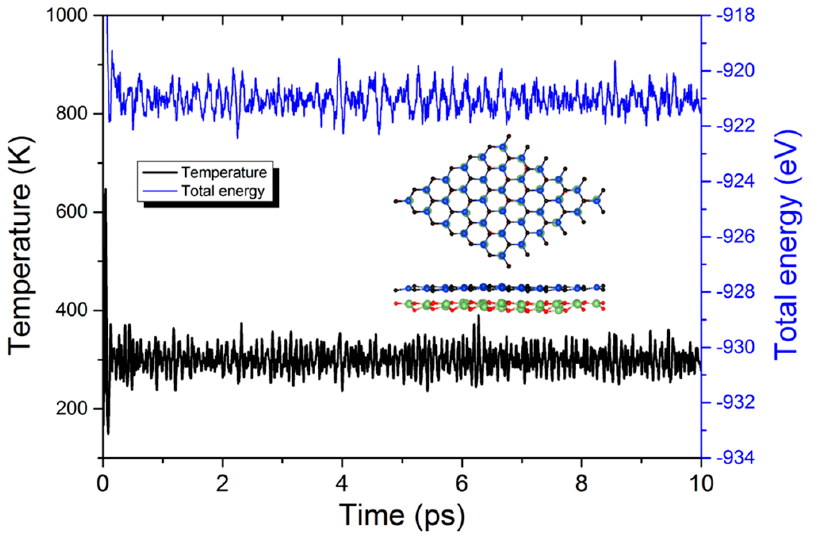
In addition to binding energy, the AIMD calculations for the SiC/GaN van der Waals heterostructure are also explored to evaluate the thermal stability using a Nosé–Hoover heat bath scheme [62]. A 6 × 6 × 1 SiC/GaN van der Waals heterostructure supercell was constructed considering the lattice translational constraints, which contains 144 atoms in the simulations [33]. Periodic boundary conditions are applied in the AIMD simulations to calculate the temperature and total energy of the SiC/GaN van der Waals heterostructure. After all the AIMD simulations at 300 K, fluctuations in temperature and total energy of the SiC/GaN van der Waals heterostructure supercell are monitored, as shown in Figure 2, suggesting a convergence of results. The structure of the relaxed SiC/GaN van der Waals heterostructure is demonstrated as the inset in Figure 2, and the SiC/GaN van der Waals heterostructure is still undamaged at 300 K after 10 ps. Thus, the SiC/GaN van der Waals heterostructure possesses an obvious thermal stability at room temperature.
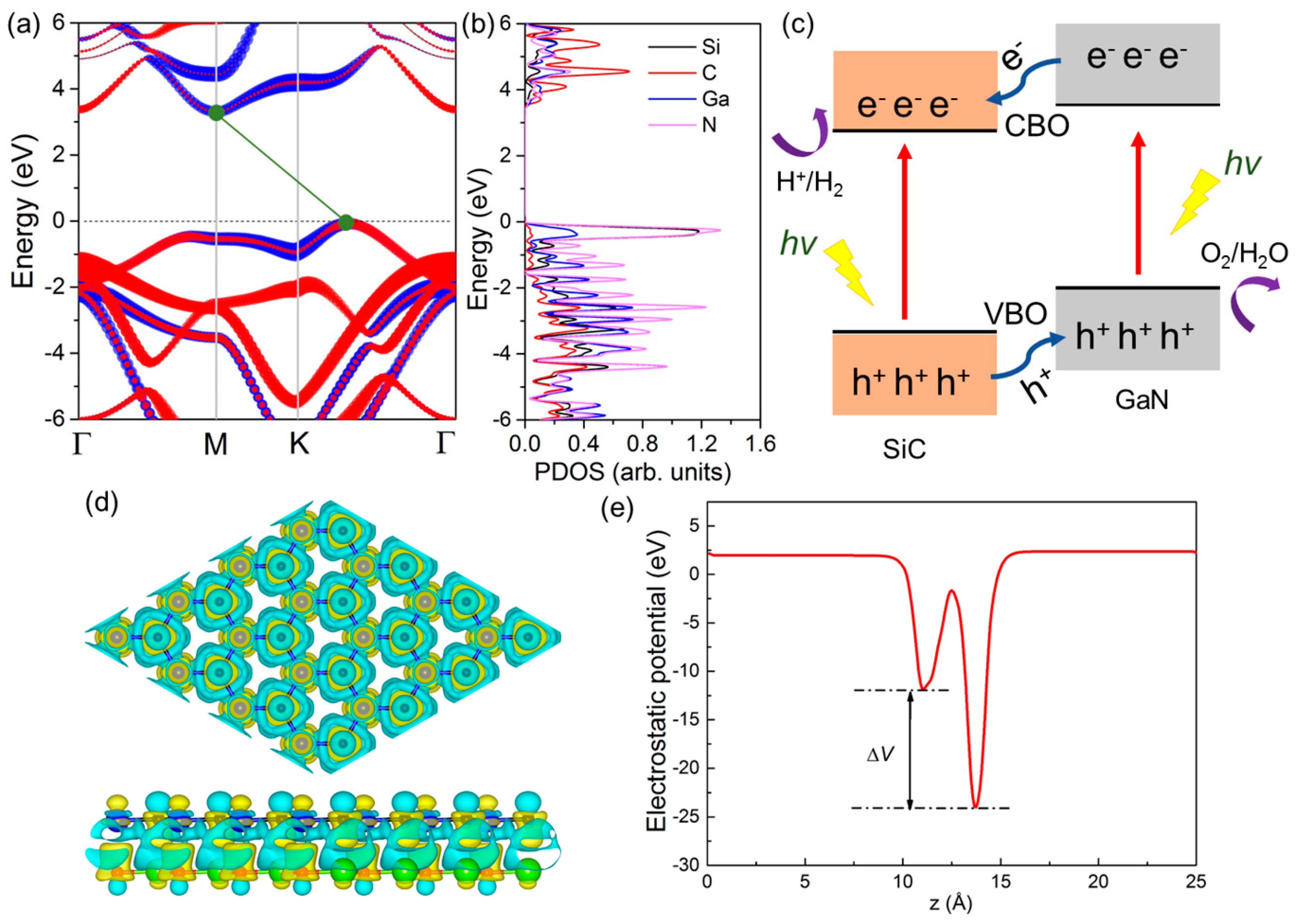
The projected band structure of the SiC/GaN van der Waals heterostructure was calculated using the HSE06 method, which is shown in Figure 3a. Obviously, the SiC/GaN van der Waals heterostructure presents a type-II band structure because the blue and red marks are donated from the SiC and GaN monolayers, respectively. Thus, the CBM and the VBM are mainly the result of the SiC and GaN monolayers, respectively. In Figure 3b, the projected density of the states of the SiC/GaN van der Waals heterostructure demonstrates that the CBM and VBM are mainly contributed by N and C, respectively. This staggered band structure means the SiC/GaN van der Waals heterostructure possesses an ability to separate the photogenerated electron and hole when used as a photocatalyst for water splitting. As shown in Figure 3c, the SiC/GaN van der Waals heterostructure obtains energy; the photogenerated electrons are stimulated from the valence band of SiC and GaN to the conduction band, resulting in a photogenerated hole at the conduction band. Then, the photogenerated electron of SiC is excited from the conduction band to the conduction band of SiC under the conduction-band offset. At the same time, the photogenerated hole in the valence band of SiC also migrates to the valence band of GaN by valence-band offset. It is worth noting that the S-scheme band structure is also a special type-II photocatalyst. The photogenerated electrons and holes in the S-scheme heterostructure migrate to the CBM–1 and VBM–1, respectively, while the photogenerated electrons and holes in the VBM and CBM at the interface combine, further enhancing the efficiency of the photocatalyst for water splitting [63,64].
Thus, the photogenerated charges can be separated in water splitting. The charge–density difference (Δρ) of the SiC/GaN van der Waals heterostructure is calculated as Δρ = ΔρSiC/GaN − ΔρSiC − ΔρGaN, where ΔρSiC/GaN, ΔρSiC, and ΔρGaN are the total charge density of the SiC/GaN van der Waals heterostructure and the SiC and GaN monolayers, respectively. As shown in Figure 3d, the SiC layer receives the charge of 0.0486 |e| by the GaN monolayer with the Bader-charge analysis [65]. Furthermore, the potential drop across the interface of the SiC/GaN van der Waals heterostructure is calculated as 12 eV, as shown in Figure 3e, which can promote a built-in electric field. Then, such a built-in electric field also can provide excellent power to separate the photogenerated charges. Interestingly, the potential drop across the interface of the SiC/GaN van der Waals heterostructure is higher than that of other 2D heterostructures that are potential photocatalysts for water splitting, such as the TMDs/BP van der Waals heterostructure [46], the TMDs/GeC van der Waals heterostructure [66], the ZnO/BSe van der Waals heterostructure [67], etc.
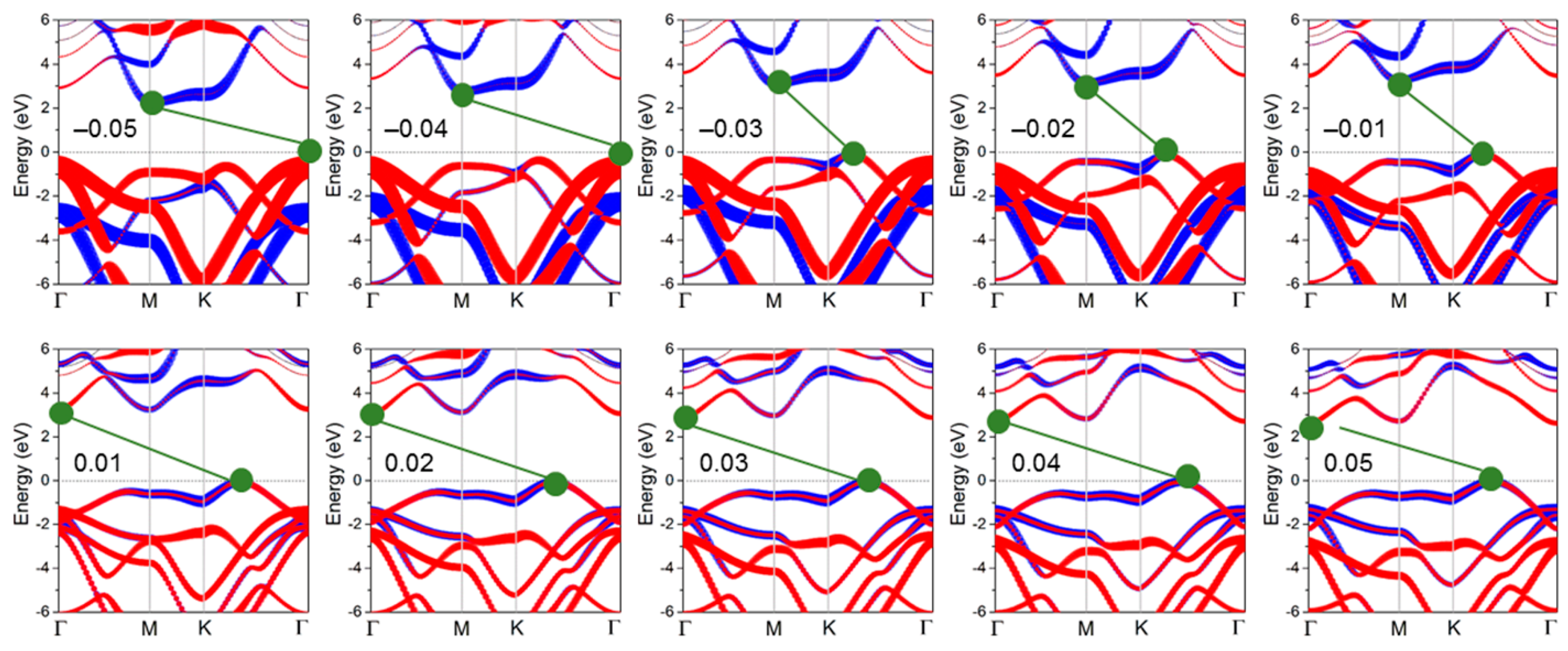
Strain engineering is an effective method to tune the properties of 2D materials and is widely used [21,68,69]. For example, external strain can induce an improved light absorption capacity of the GaN/BSe van der Waals heterostructure when used as a photocatalyst for water splitting [60]. The mechanical properties of the SiP2 monolayer can also be tuned with external strain for potential nanomechanics and nanoelectronics [70]. Applied strain is also particularly important for the fracture behavior of 2D materials [69]. In this work, we also applied external biaxial and in-plane strain on the SiC/GaN van der Waals heterostructure to explore the potential applications. Here, tension is expressed as a positive number, while the pressure is positive. The calculated projected band structure of the SiC/GaN van der Waals heterostructure under external strain from –0.05 to 0.05 is shown in Figure 4. Interestingly, the band structure of the SiC/GaN van der Waals heterostructure shows clear feedback to the external biaxial strain. Compared with Figure 3a, when tensile stress is applied to the SiC/GaN van der Waals heterostructure, the contribution of the Ga monolayer to the CBM gradually strengthens, which means the SiC/GaN van der Waals heterostructure is changed to a type-I semiconductor. The type-I SiC/GaN van der Waals heterostructure can be used as a light-emitting device material [71]. On the contrary, when the compression force is applied to the SiC/GaN van der Waals heterostructure, the CBM and VBM are completely donated by the SiC and GaN monolayers, suggesting a pure type-II band structure. Thus, the SiC/GaN van der Waals heterostructure under compression force is more suitable for separating the photogenerated electron and hole. In addition, the VBM of the SiC/GaN van der Waals heterostructure is also transformed from the middle of the K and Γ point to the Γ point. The dependence of the CBM and the VBM of the C/GaN van der Waals heterostructure on external strain is also mainly decided by the dependence of the SiC and GaN monolayers on the strain because their combination is due to weak van der Waals forces. Thus, it is obvious that the CBM and the VBM of the SiC and GaN monolayers are particularly sensitive to external strain, suggesting the tunable carrier mobility with strain. All these indicate that the SiC/GaN van der Waals heterostructure can be used in more applications involving external biaxial strain. Furthermore, such a pronounced strain dependence on the band structure of the SiC/GaN van der Waals heterostructure also shows a potential application in piezoelectric photocatalysts [72].
The band edge positions of the SiC/GaN van der Waals heterostructure are calculated with different external biaxial strains, as shown in Figure 5a. One can see that the SiC/GaN van der Waals heterostructure possesses decent band alignment to induce the redox (−5.67 eV for oxidation and −4.44 eV for reduction) water splitting at pH 0 under 0–0.05 strain. At the same time, the potential for reduction and oxidation also can be determined by the pH level using Ered = −4.44 eV + pH × 0.059 eV and Eoxd = −5.67 eV + pH × 0.059 eV, respectively [60]. Thus, the SiC/GaN van der Waals heterostructure under −0.04 to 0.05 strain also can promote water oxidation (−5.26 eV) and reduction (−4.03 eV) at pH = 7 for water splitting. The total energy of the system and the bandgap of the stained SiC/GaN van der Waals heterostructure are shown in Figure 5b. The SiC/GaN system without any external strain shows the lowest energy. Interestingly, the bandgap of the SiC/GaN van der Waals heterostructure can decrease with both tension and pressure.
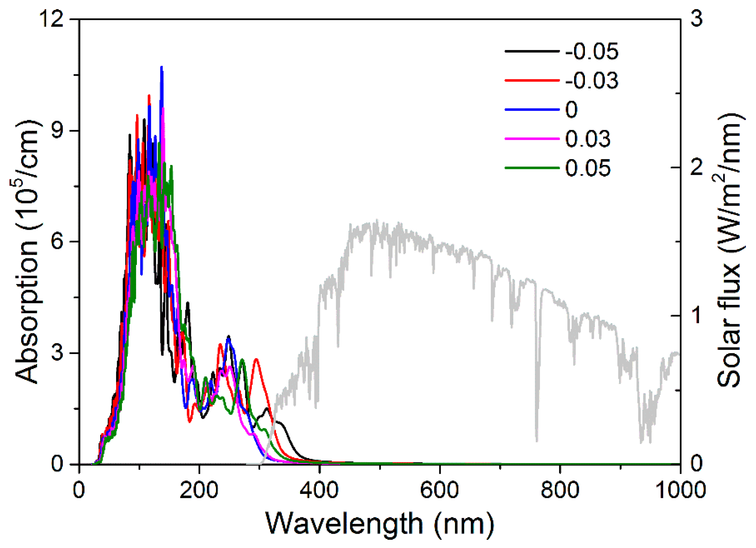
The optical absorption capacity for the SiC/GaN van der Waals heterostructure is a critical property used as a photocatalyst to decompose water. The absorption coefficient of the SiC/GaN van der Waals heterostructure is calculated as , where is used as the dielectric constant, while is used to show the imaginary parts of the dielectric constant. Furthermore, ω is decided by the angular frequency, α represents the absorption coefficient, and c is the speed of light in vacuum [71]. Then, the optical absorption spectrum of the SiC/GaN van der Waals heterostructure under the different external biaxial strains is calculated, as shown in Figure 6, using the HSE06 functional. One can see that when the SiC/GaN van der Waals heterostructure is out of strain, the excellent absorption peak near the visible light region is 3.4 × 105 cm−1 at the wavelength of 250 nm. External strain obviously enhances the light absorption ability: the absorption peak of the SiC/GaN van der Waals heterostructure is 2.8 × 105 cm−1, and the absorption peak position is in the visible light range (305 nm) with a strain of −0.03. At the same time, the absorption peak of the SiC/GaN van der Waals heterostructure even moves to 313 nm with an absorption peak of 1.5 × 105 cm−1. The absorption peak position of the SiC/GaN van der Waals heterostructure can also be enhanced to 270 nm with the absorption peak of 2.8 × 105 cm−1. All these obtained optical absorptions of the SiC/GaN van der Waals heterostructure are more advantageous than the other 2D heterostructures used as photocatalysts for water splitting, such as the CdO/As van der Waals heterostructure (about 8.47 × 104 cm−1) [73] and MoTe2/PtS2 (about 2.6 × 105 cm−1) [68].
4. Conclusions
In summary, density functional theory is conducted to systematically investigate structural performances. The most stable stacking figuration is formed by van der Waals interactions, and thermal stability is also obtained with AIMD simulation. Then, the SiC/GaN van der Waals heterostructure is calculated as a type-II semiconductor with an indirect bandgap of 3.331 eV to separate the photogenerated electrons and holes, acting as a photocatalyst for water splitting. Importantly, even if the SiC/GaN van der Waals heterostructure maintains semiconductor characteristics, it presents an indirect bandgap from type-II to type-I with external biaxial strain. Furthermore, the strain also can decrease the bandgap of the SiC/GaN van der Waals heterostructure. The SiC/GaN van der Waals heterostructure has decent band edge energy for the redox of water splitting under the external biaxial strain at pH 0 and 7, the optical properties also can be enhanced with external strain, implying its efficient and tunable application as photocatalyst and nanoelectronics. In addition, the SiC or GaN monolayer stacked on Janus materials may present other interesting photocatalytic properties. For example, Janus TMDs possess excellent optical properties. The Janus materials-based heterostructure presents a built-in electric field in such an asymmetric structure, which can form a more favorable photogenerated charge flow mode formed with GaN or SiC. For GaN- or SiC-based heterostructures with TMD materials (such as WS2), the closest atom to GaN or SiC is the S atom. Thus, it may be a good strategy to regulate the vibration mode of S atoms to induce a heterostructure photocatalytic effect.
Supplementary Materials
The following supporting information can be downloaded at: https://0-www-mdpi-com.brum.beds.ac.uk/article/10.3390/cryst14010030/s1, Figure S1: The band structure of the SiC and GaN monolayers calculated with HSE06 function; Figure S2: The bond strain of the SiC and GaN monolayers.
Author Contributions
Conceptualization, L.Z.; methodology, R.Z. and H.P.; software, R.Z.; validation, R.Z.; formal analysis, L.W., H.S. and R.Z.; investigation, W.M. and H.P.; resources, L.Z.; data curation, L.Z.; writing—original draft preparation, L.Z.; writing—review and editing, H.S.; visualization, H.S.; supervision, W.M.; project administration, H.P.; funding acquisition, L.Z. and W.M. All authors have read and agreed to the published version of the manuscript.
Funding
The authors gratefully acknowledge the financial support of the Key Natural Science Research Projects of Anhui Provincial Higher Education Institutions (Project numbers: 2022AH052368, 2022AH052431), the Shenzhen Polytechnic Research Fund (Project number: 6023310003k), and the Scientific Research Revitalization Plan Projects of Higher Education Institutions (Project number: ZXTS202202). W.M. thanks the startup grant from Wenzhou Institute, University of Chinese Academy of Sciences (No. WIUCASQD2021024).
Data Availability Statement
The data presented in this study are available in the article.
Conflicts of Interest
The authors declare that they have no competing interest.
References
- Geim, A.K.; Novoselov, K.S. The rise of graphene. Nat. Mater. 2007, 6, 183–191. [Google Scholar] [CrossRef]
- Martinez-Canales, M.; Galeev, T.R.; Boldyrev, A.I.; Pickard, C.J. Dirac cones in two-dimensional borane. Phys. Rev. B 2017, 96, 195442. [Google Scholar] [CrossRef]
- Zhou, H.; Yu, W.J.; Liu, L.; Cheng, R.; Chen, Y.; Huang, X.; Liu, Y.; Wang, Y.; Huang, Y.; Duan, X. Chemical vapour deposition growth of large single crystals of monolayer and bilayer graphene. Nat. Commun. 2013, 4, 2096. [Google Scholar] [CrossRef] [PubMed]
- Jiang, J.; Sun, F.; Zhou, S.; Hu, W.; Zhang, H.; Dong, J.; Jiang, Z.; Zhao, J.; Li, J.; Yan, W. Atomic-level insight into super-efficient electrocatalytic oxygen evolution on iron and vanadium co-doped nickel (oxy) hydroxide. Nat. Commun. 2018, 9, 2885. [Google Scholar] [CrossRef]
- Liu, Q.; Xing, J.; Jiang, Z.; Jiang, X.; Wang, Y.; Zhao, J. 2D tetragonal transition-metal phosphides: An ideal platform to screen metal shrouded crystals for multifunctional applications. Nanoscale 2020, 12, 6776–6784. [Google Scholar] [CrossRef] [PubMed]
- He, Z.; Li, L.; Ma, H.; Pu, L.; Xu, H.; Yi, Z.; Cao, X.; Cui, W. Graphene-based metasurface sensing applications in terahertz band. Results Phys. 2021, 21, 103795. [Google Scholar] [CrossRef]
- Ren, K.; Ma, X.; Liu, X.; Xu, Y.; Huo, W.; Li, W.; Zhang, G. Prediction of 2D IV–VI semiconductors: Auxetic materials with direct bandgap and strong optical absorption. Nanoscale 2022, 14, 8463–8473. [Google Scholar] [CrossRef]
- Ma, X.; Liu, J.; Fan, Y.; Li, W.; Hu, J.; Zhao, M. Giant negative Poisson’s ratio in two-dimensional V-shaped materials. Nanoscale Adv. 2021, 3, 4554–4560. [Google Scholar] [CrossRef]
- Zhang, G.; Zhang, Y.-W. Thermoelectric properties of two-dimensional transition metal dichalcogenides. J. Mater. Chem. C 2017, 5, 7684–7698. [Google Scholar] [CrossRef]
- Ren, K.; Shu, H.; Wang, K.; Qin, H. Two-dimensional MX2Y4 systems: Ultrahigh carrier transport and excellent hydrogen evolution reaction performances. Phys. Chem. Chem. Phys. 2023, 25, 4519–4527. [Google Scholar] [CrossRef]
- Lu, A.-Y.; Zhu, H.; Xiao, J.; Chuu, C.-P.; Han, Y.; Chiu, M.-H.; Cheng, C.-C.; Yang, C.-W.; Wei, K.-H.; Yang, Y.; et al. Janus monolayers of transition metal dichalcogenides. Nat. Nanotechnol. 2017, 12, 744–749. [Google Scholar] [CrossRef] [PubMed]
- Ren, K.; Wang, K.; Cheng, Y.; Tang, W.; Zhang, G. Two-dimensional heterostructures for photocatalytic water splitting: A review of recent progress. Nano Futur. 2020, 4, 032006. [Google Scholar] [CrossRef]
- Safari, F.; Moradinasab, M.; Fathipour, M.; Kosina, H. Adsorption of the NH3, NO, NO2, CO2, and CO gas molecules on blue phosphorene: A first-principles study. Appl. Surf. Sci. 2019, 464, 153–161. [Google Scholar] [CrossRef]
- Li, Y.; Chen, X. Dirac fermions in blue-phosphorus. 2D Mater. 2014, 1, 031002. [Google Scholar] [CrossRef]
- Deng, Z.; Li, Z.; Wang, W.; She, J. Vibrational properties and Raman spectra of pristine and fluorinated blue phosphorene. Phys. Chem. Chem. Phys. 2019, 21, 1059–1066. [Google Scholar] [CrossRef] [PubMed]
- Xiao, J.; Long, M.; Deng, C.-S.; He, J.; Cui, L.-L.; Xu, H. Electronic Structures and Carrier Mobilities of Blue Phosphorus Nanoribbons and Nanotubes: A First-Principles Study. J. Phys. Chem. C 2016, 120, 4638–4646. [Google Scholar] [CrossRef]
- Sun, M.; Hao, Y.; Ren, Q.; Zhao, Y.; Du, Y.; Tang, W. Tuning electronic and magnetic properties of blue phosphorene by doping Al, Si, As and Sb atom: A DFT calculation. Solid State Commun. 2016, 242, 36–40. [Google Scholar] [CrossRef]
- Ren, K.; Shu, H.; Huang, L.; Wang, K.; Luo, Y.; Huo, W.; Bi, C.; Jing, Y. Predicted XN (X = C, Si, Ge, and Sn) Monolayers with Ultrahigh Carrier Mobility: Potential Photocatalysts for Water Splitting. J. Phys. Chem. C 2023, 127, 21006–21014. [Google Scholar] [CrossRef]
- Hao, A.; Yang, X.; Wang, X.; Zhu, Y.; Liu, X.; Liu, R. First-principles investigations on electronic, elastic and optical properties of XC (X = Si, Ge, and Sn) under high pressure. J. Appl. Phys. 2010, 108, 063531. [Google Scholar] [CrossRef]
- Peng, Q.; Liang, C.; Ji, W.; De, S. Mechanical properties of g-GaN: A first principles study. Appl. Phys. A 2013, 113, 483–490. [Google Scholar] [CrossRef]
- Huang, L.; Ren, K.; Zhang, H.; Qin, H. Enhanced mechanical and the thermal properties of the two-dimensional XC (X = Si and Ge) with temperature and size dependence. Chin. Phys. B 2023, 32, 076103. [Google Scholar] [CrossRef]
- Ren, K.; Ding, B.; Zhang, G. Editorial for Special Issue “Dynamics and Mechanics in Two-Dimensional Nanostructures: Simulation and Computation”. Nanomaterials 2023, 13, 400. [Google Scholar] [CrossRef]
- Luo, Z.; Maassen, J.; Deng, Y.; Du, Y.; Garrelts, R.P.; Lundstrom, M.S.; Ye, P.D.; Xu, X. Anisotropic in-plane thermal conductivity observed in few-layer black phosphorus. Nat. Commun. 2015, 6, 8572. [Google Scholar] [CrossRef] [PubMed]
- Zhang, G.; Zhang, Y.-W. Thermal properties of two-dimensional materials. Chin. Phys. B 2017, 26, 34401. [Google Scholar] [CrossRef]
- Hong, Y.; Zhang, J.; Huang, X.; Zeng, X.C. Thermal conductivity of a two-dimensional phosphorene sheet: A comparative study with graphene. Nanoscale 2015, 7, 18716–18724. [Google Scholar] [CrossRef] [PubMed]
- Peng, Q.; Liang, C.; Ji, W.; De, S. A first-principles study of the mechanical properties of g-GeC. Mech. Mater. 2013, 64, 135–141. [Google Scholar] [CrossRef]
- Pandey, R.; Rérat, M.; Darrigan, C.; Causa, M. A theoretical study of stability, electronic, and optical properties of GeC and SnC. J. Appl. Phys. 2000, 88, 6462–6466. [Google Scholar] [CrossRef]
- Radisavljevic, B.; Radenovic, A.; Brivio, J.; Giacometti, V.; Kis, A. Single-layer MoS2 transistors. Nat. Nanotechnol. 2011, 6, 147–150. [Google Scholar] [CrossRef] [PubMed]
- Liu, G.; Gan, Y.; Quhe, R.; Lu, P. Strain dependent electronic and optical properties of PtS2 monolayer. Chem. Phys. Lett. 2018, 709, 65–70. [Google Scholar] [CrossRef]
- Zhao, D.; Xie, S.; Wang, Y.; Zhu, H.; Chen, L.; Sun, Q.; Zhang, D.W. Synthesis of large-scale few-layer PtS2 films by chemical vapor deposition. AIP Adv. 2019, 9, 025225. [Google Scholar] [CrossRef]
- Ren, K.; Chen, H.; Sun, H.; Wang, Q.; Sun, Q.; Jin, B. Design and Analysis of a Permanent Magnet Brushless DC Motor in an Automotive Cooling System. World Electr. Veh. J. 2023, 14, 228. [Google Scholar] [CrossRef]
- Ren, K.; Zhang, S.; Zhang, H.; Deng, C.; Sun, H. Flow field analysis and noise characteristics of an automotive cooling fan at different speeds. Front. Energy Res. 2023, 11, 1259052. [Google Scholar] [CrossRef]
- Zhang, C.; Ren, K.; Wang, S.; Luo, Y.; Tang, W.; Sun, M. Recent progress on two-dimensional van der Waals heterostructures for photocatalytic water splitting: A selective review. J. Phys. D Appl. Phys. 2023, 56, 483001. [Google Scholar] [CrossRef]
- Kumar, S.; Sharma, S.; Karmaker, R.; Sinha, D. DFT study on the structural, optical and electronic properties of platinum group doped graphene. Mater. Today Commun. 2021, 26, 101755. [Google Scholar] [CrossRef]
- Novoselov, K.S.; Mishchenko, A.; Carvalho, A.; Castro Neto, A.H. 2D materials and van der Waals heterostructures. Science 2016, 353, aac9439. [Google Scholar] [CrossRef]
- Luo, Y.; Ren, K.; Wang, S.; Chou, J.-P.; Yu, J.; Sun, Z.; Sun, M. First-Principles Study on Transition-Metal Dichalcogenide/BSe van der Waals Heterostructures: A Promising Water-Splitting Photocatalyst. J. Phys. Chem. C 2019, 123, 22742–22751. [Google Scholar] [CrossRef]
- Luo, Y.; Wang, S.; Shu, H.; Chou, J.P.; Ren, K.; Yu, J.; Sun, M. A MoSSe/blue phosphorene vdw heterostructure with energy conversion efficiency of 19.9% for photocatalytic water splitting. Semicond. Sci. Technol. 2020, 35, 125008. [Google Scholar] [CrossRef]
- Luo, Y.; Wang, S.; Ren, K.; Chou, J.P.; Yu, J.; Sun, Z.; Sun, M. Transition-metal dichalcogenides/Mg(OH)2 van der Waals heterostructures as promising water-splitting photocatalysts: A first-principles study. Phys. Chem. Chem. Phys. 2019, 21, 1791–1796. [Google Scholar] [CrossRef] [PubMed]
- Wang, H.; Li, X.; Li, P.; Yang, J. δ-Phosphorene: A two dimensional material with a highly negative Poisson’s ratio. Nanoscale 2017, 9, 850–855. [Google Scholar] [CrossRef]
- Fan, Y.; Yang, B.; Song, X.; Shao, X.; Zhao, M. Direct Z-scheme photocatalytic overall water splitting on 2D CdS/InSe heterostructures. J. Phys. Phys. D Appl. Phys. 2018, 51, 395501. [Google Scholar] [CrossRef]
- Zhu, M.; Sun, Z.; Fujitsuka, M.; Majima, T. Z-Scheme Photocatalytic Water Splitting on a 2D Heterostructure of Black Phosphorus/Bismuth Vanadate Using Visible Light. Angew. Chem. 2018, 57, 2160–2164. [Google Scholar] [CrossRef]
- Shi, E.; Yuan, B.; Shiring, S.B.; Gao, Y.; Akriti; Guo, Y.; Su, C.; Lai, M.; Yang, P.; Kong, J.; et al. Two-dimensional halide perovskite lateral epitaxial heterostructures. Nature 2020, 580, 614–620. [Google Scholar] [CrossRef] [PubMed]
- Bellus, M.Z.; Li, M.; Lane, S.D.; Ceballos, F.; Cui, Q.; Zeng, X.C.; Zhao, H. Type-I van der Waals heterostructure formed by MoS2 and ReS2 monolayers. Nanoscale Horiz 2017, 2, 31–36. [Google Scholar] [CrossRef] [PubMed]
- Wang, B.-J.; Li, X.-H.; Zhao, R.; Cai, X.-L.; Yu, W.-Y.; Li, W.-B.; Liu, Z.-S.; Zhang, L.-W.; Ke, S.-H. Electronic structures and enhanced photocatalytic properties of blue phosphorene/BSe van der Waals heterostructures. J. Mater. Chem. A 2018, 6, 8923–8929. [Google Scholar] [CrossRef]
- Fu, C.-F.; Li, X.; Yang, J. A rationally designed two-dimensional MoSe2/Ti2CO2 heterojunction for photocatalytic overall water splitting: Simultaneously suppressing electron–hole recombination and photocorrosion. Chem. Sci. 2021, 12, 2863–2869. [Google Scholar] [CrossRef]
- Ren, K.; Sun, M.; Luo, Y.; Wang, S.; Yu, J.; Tang, W. First-principle study of electronic and optical properties of two-dimensional materials-based heterostructures based on transition metal dichalcogenides and boron phosphide. Appl. Surf. Sci. 2019, 476, 70–75. [Google Scholar] [CrossRef]
- Doustkhah, E.; Hassandoost, R.; Tizhoosh, N.Y.; Esmat, M.; Guselnikova, O.; Assadi, M.H.N.; Khataee, A. Ultrasonically-assisted synthesis of CeO2 within WS2 interlayers forming type II heterojunction for a VOC photocatalytic oxidation. Ultrason. Sonochemistry 2023, 92, 106245. [Google Scholar] [CrossRef] [PubMed]
- Polley, C.M.; Fedderwitz, H.; Balasubramanian, T.; Zakharov, A.A.; Yakimova, R.; Bäcke, O.; Ekman, J.; Dash, S.P.; Kubatkin, S.; Lara-Avila, S. Bottom-Up Growth of Monolayer Honeycomb SiC. Phys. Rev. Lett. 2023, 130, 076203. [Google Scholar] [CrossRef]
- Ren, K.; Ren, C.; Luo, Y.; Xu, Y.; Yu, J.; Tang, W.; Sun, M. Using van der Waals heterostructures based on two-dimensional blue phosphorus and XC (X = Ge, Si) for water-splitting photocatalysis: A first-principles study. Phys. Chem. Chem. Phys. 2019, 21, 9949–9956. [Google Scholar] [CrossRef]
- Onen, A.; Kecik, D.; Durgun, E.; Ciraci, S. GaN: From three- to two-dimensional single-layer crystal and its multilayer van der Waals solids. Phys. Rev. B 2016, 93, 085431. [Google Scholar] [CrossRef]
- ZAl Balushi, Z.Y.; Wang, K.; Ghosh, R.K.; Vilá, R.A.; Eichfeld, S.M.; Caldwell, J.D.; Qin, X.; Lin, Y.-C.; DeSario, P.A.; Stone, G.; et al. Two-dimensional gallium nitride realized via graphene encapsulation. Nat. Mater. 2016, 15, 1166–1171. [Google Scholar] [CrossRef]
- Lou, J.; Ren, K.; Huang, Z.; Huo, W.; Zhu, Z.; Yu, J. Electronic and optical properties of two-dimensional heterostructures based on Janus XSSe (X = Mo, W) and Mg(OH)2: A first principles investigation. RSC Adv. 2021, 11, 29576–29584. [Google Scholar] [CrossRef] [PubMed]
- Ren, K.; Wang, S.; Luo, Y.; Chou, J.P.; Yu, J.; Tang, W.; Sun, M. High-efficiency photocatalyst for water splitting: A Janus MoSSe/XN (X = Ga, Al) van der Waals heterostructure. J. Phys. Phys. D Appl. Phys. 2020, 53, 185504. [Google Scholar] [CrossRef]
- Din, H.U.; Idrees, M.; Rehman, G.; Nguyen, C.V.; Gan, L.Y.; Ahmad, I.; Maqbool, M.; Amin, B. Electronic structure, optical and photocatalytic performance of SiC-MX2 (M = Mo, W and X = S, Se) van der Waals heterostructures. Phys. Chem. Chem. Phys. 2018, 20, 24168–24175. [Google Scholar] [CrossRef] [PubMed]
- Capelle, K. A bird’s-eye view of density-functional theory. Braz. J. Phys. 2006, 36, 1318–1343. [Google Scholar] [CrossRef]
- Grimme, S.; Antony, J.; Ehrlich, S.; Krieg, H. A consistent and accurate ab initio parametrization of density functional dispersion correction (DFT-D) for the 94 elements H-Pu. J. Chem. Phys. 2010, 132, 154104. [Google Scholar] [CrossRef] [PubMed]
- Kresse, G.; Furthmüller, J. Efficiency of ab-initio total energy calculations for metals and semiconductors using a plane-wave basis set. Comput. Mater. Sci. 1996, 6, 15–50. [Google Scholar] [CrossRef]
- Tang, W.; Sanville, E.; Henkelman, G. A grid-based Bader analysis algorithm without lattice bias. J. Physics. Condens. Matter Inst. Phys. J. 2009, 21, 084204. [Google Scholar] [CrossRef]
- Heyd, J.; Peralta, J.E.; Scuseria, G.E.; Martin, R.L. Energy band gaps and lattice parameters evaluated with the Heyd-Scuseria-Ernzerhof screened hybrid functional. J. Chem. Phys. 2005, 123, 174101. [Google Scholar] [CrossRef]
- Ren, K.; Luo, Y.; Wang, S.; Chou, J.-P.; Yu, J.; Tang, W.; Sun, M. A van der Waals Heterostructure Based on Graphene-like Gallium Nitride and Boron Selenide: A High-Efficiency Photocatalyst for Water Splitting. ACS Omega 2019, 4, 21689–21697. [Google Scholar] [CrossRef]
- Chen, X.; Tian, F.; Persson, C.; Duan, W.; Chen, N.-X. Interlayer interactions in graphites. Sci. Rep. 2013, 3, 3046. [Google Scholar] [CrossRef]
- Nosé, S. A unified formulation of the constant temperature molecular dynamics methods. J. Chem. Phys. 1984, 81, 511–519. [Google Scholar] [CrossRef]
- Zhang, Q.; Ren, K.; Zheng, R.; Huang, Z.; An, Z.; Cui, Z. First-principles calculations of two-dimensional CdO/HfS2 van der Waals heterostructure: Direct Z-scheme photocatalytic water splitting. Front. Chem. 2022, 10, 879402. [Google Scholar] [CrossRef]
- Bard, A. Photoelectrochemistry and heterogeneous photocatalysis at semiconductors. J. Photochem. 1979, 10, 59–75. [Google Scholar] [CrossRef]
- Henkelman, G.; Arnaldsson, A.; Jónsson, H. A fast and robust algorithm for Bader decomposition of charge density. Comput. Mater. Sci. 2006, 36, 354–360. [Google Scholar] [CrossRef]
- Ren, K.; Yu, J.; Tang, W. First-principles study of two-dimensional van der Waals heterostructure based on ZnO and Mg(OH)2: A potential photocatalyst for water splitting. Phys. A 2019, 383, 125916. [Google Scholar] [CrossRef]
- Ren, K.; Yu, J.; Tang, W. Two-dimensional ZnO/BSe van der waals heterostructure used as a promising photocatalyst for water splitting: A DFT study. J. Alloys Compd. 2020, 812, 152049. [Google Scholar] [CrossRef]
- Zhang, L.; Ren, K.; Cheng, H.; Cui, Z.; Li, J. The First-Principles Study of External Strain Tuning the Electronic and Optical Properties of the 2D MoTe2/PtS2 van der Waals Heterostructure. Front. Chem. 2022, 10, 934048. [Google Scholar] [CrossRef] [PubMed]
- Ren, K.; Zhang, G.; Zhang, L.; Qin, H.; Zhang, G. Ultraflexible two-dimensional Janus heterostructure superlattice: A novel intrinsic wrinkled structure. Nanoscale 2023, 15, 8654–8661. [Google Scholar] [CrossRef]
- Hou, Y.; Ren, K.; Wei, Y.; Yang, D.; Cui, Z.; Wang, K. Anisotropic Mechanical Properties of Orthorhombic SiP2 Monolayer: A First-Principles Study. Molecules 2023, 28, 6514. [Google Scholar] [CrossRef]
- Ren, K.; Zheng, R.; Lou, J.; Yu, J.; Sun, Q.; Li, J. Ab Initio Calculations for the Electronic, Interfacial and Optical Properties of Two-Dimensional AlN/Zr2CO2 Heterostructure. Front. Chem. 2021, 9, 796695. [Google Scholar] [CrossRef] [PubMed]
- Liu, Z.; Wang, B.; Chu, D.; Cazorla, C. First-principles high-throughput screening of bulk piezo-photocatalytic materials for sunlight-driven hydrogen production. J. Mater. Chem. A 2022, 10, 18132–18146. [Google Scholar] [CrossRef]
- Ren, K.; Zheng, R.; Yu, J.; Sun, Q.; Li, J. Band Bending Mechanism in CdO/Arsenene Heterostructure: A Potential Direct Z-scheme Photocatalyst. Front. Chem. 2021, 9, 788813. [Google Scholar] [CrossRef]
Figure 1.
The geometric structure of the SiC/GaN heterostructure stacked with the (a) G1, (b) G2, (c) G3, (d) G4, (e) G5, and (f) G6 stacking styles. The blue, black, cyan, and red balls represent Si, C, Ga, and N atoms, respectively.
Figure 1.
The geometric structure of the SiC/GaN heterostructure stacked with the (a) G1, (b) G2, (c) G3, (d) G4, (e) G5, and (f) G6 stacking styles. The blue, black, cyan, and red balls represent Si, C, Ga, and N atoms, respectively.

Figure 2.
The total energy and temperature of the AIMD calculation. The inset is the relaxed structure of the SiC/GaN van der Waals heterostructure at 300 K.
Figure 2.
The total energy and temperature of the AIMD calculation. The inset is the relaxed structure of the SiC/GaN van der Waals heterostructure at 300 K.

Figure 3.
(a) The calculated projected band structure and the (b) projected density of the states of the SiC/GaN van der Waals heterostructure, the blue and red marks are SiC and GaN, respectively. (c) In the photogenerated charge flow diagram of the SiC/GaN van der Waals heterostructure, CBO and VBO represent the conduction-band offset and the valence-band offset, respectively. (d) The charge density of the SiC/GaN van der Waals heterostructure and the gain and loss of electrons are indicated with yellow and blue symbols, respectively. (e) The potential drop across the interface of the SiC/GaN van der Waals heterostructure.

Figure 4.
The calculated projected band structure of the SiC/GaN van der Waals heterostructure under different external biaxial strain. The blue and red marks are SiC and GaN, respectively.
Figure 4.
The calculated projected band structure of the SiC/GaN van der Waals heterostructure under different external biaxial strain. The blue and red marks are SiC and GaN, respectively.

Figure 5.
(a) The band alignment and (b) the energy and bandgap of the SiC/GaN van der Waals heterostructure under different external biaxial strains.
Figure 5.
(a) The band alignment and (b) the energy and bandgap of the SiC/GaN van der Waals heterostructure under different external biaxial strains.

Figure 6.
The obtained optical absorption of the SiC/GaN van der Waals heterostructure under different external biaxial strains.
Figure 6.
The obtained optical absorption of the SiC/GaN van der Waals heterostructure under different external biaxial strains.


Table 1.
The calculated binding energy (Eb, meV/unit), the optimized bond length (B, Å), and the interfacial height (h, Å) of the SiC/GaN van der Waals heterostructure constructed with different stacking styles.
Table 1.
The calculated binding energy (Eb, meV/unit), the optimized bond length (B, Å), and the interfacial height (h, Å) of the SiC/GaN van der Waals heterostructure constructed with different stacking styles.
| G1 | G1 | G1 | G1 | G1 | G1 | |
|---|---|---|---|---|---|---|
| Eb | −133 | –174 | –53 | –170 | –21 | –41 |
| BGa–N | 1.832 | 1.836 | 1.832 | 1.832 | 1.832 | 1.832 |
| BSi–C | 1.832 | 1.834 | 1.832 | 1.832 | 1.832 | 1.832 |
| h | 4.853 | 2.528 | 3.505 | 4.893 | 4.170 | 3.583 |
Disclaimer/Publisher’s Note: The statements, opinions and data contained in all publications are solely those of the individual author(s) and contributor(s) and not of MDPI and/or the editor(s). MDPI and/or the editor(s) disclaim responsibility for any injury to people or property resulting from any ideas, methods, instructions or products referred to in the content. |
© 2023 by the authors. Licensee MDPI, Basel, Switzerland. This article is an open access article distributed under the terms and conditions of the Creative Commons Attribution (CC BY) license (https://creativecommons.org/licenses/by/4.0/).
Share and Cite
MDPI and ACS Style
Zhang, L.; Sun, H.; Zheng, R.; Pan, H.; Mu, W.; Wang, L. The Transition from Type-I to Type-II SiC/GaN Heterostructure with External Strain. Crystals 2024, 14, 30. https://0-doi-org.brum.beds.ac.uk/10.3390/cryst14010030
AMA Style
Zhang L, Sun H, Zheng R, Pan H, Mu W, Wang L. The Transition from Type-I to Type-II SiC/GaN Heterostructure with External Strain. Crystals. 2024; 14(1):30. https://0-doi-org.brum.beds.ac.uk/10.3390/cryst14010030
Chicago/Turabian StyleZhang, Li, Haiyang Sun, Ruxin Zheng, Hao Pan, Weihua Mu, and Li Wang. 2024. "The Transition from Type-I to Type-II SiC/GaN Heterostructure with External Strain" Crystals 14, no. 1: 30. https://0-doi-org.brum.beds.ac.uk/10.3390/cryst14010030
Note that from the first issue of 2016, this journal uses article numbers instead of page numbers. See further details here.