Reconfigurable Topological Phases in Two-Dimensional Dielectric Photonic Crystals


State Key Laboratory of Advanced Design and Manufacturing for Vehicle Body, College of Mechanical and Vehicle Engineering, Hunan University, Changsha 410082, China
*
Author to whom correspondence should be addressed.
Crystals 2019, 9(4), 221; https://0-doi-org.brum.beds.ac.uk/10.3390/cryst9040221
Submission received: 1 March 2019
/
Revised: 17 April 2019
/
Accepted: 19 April 2019
/
Published: 24 April 2019
(This article belongs to the Special Issue Recent Advances in Novel Topological Materials)
Abstract
:The extensive research on photonic topological insulators has opened up an intriguing way to control electromagnetic (EM) waves. In this work, we numerically demonstrate reconfigurable microwave photon analogues of topological insulator (TIs) in a triangular lattice of elliptical cylinders, according to the theory of topological defects. Multiple topological transitions between the trivial and nontrivial photonic phases can be realized by inhomogeneously changing the ellipse orientation, without altering the lattice structure. Topological protection of the edge states and reconfigurable topological one-way propagation at microwave frequencies, are further verified. Our approach provides a new route towards freely steering light propagations in dielectric photonic crystals (PCs), which has potential applications in the areas of topological signal processing and sensing.
1. Introduction
The discovery of topological phases of matter is one of the most exciting advancements inspired by quantum systems [1,2,3,4]. Since then, the concept of nontrivial topological physics has been introduced to classical systems, such as topological acoustic [5,6,7], and elastic waves systems [8,9,10], with particular interests focusing on achieving one-way protected edge states that are immune to backscattering. In recent years, photonic equivalents of condensed matter topological insulator (TIs) have led to unprecedented opportunities in the control of EM waves [11,12,13,14,15], and a variety of theoretical and experimental demonstrations have been reported from microwaves to optical waves [16,17,18,19,20,21,22,23,24,25,26,27,28,29]. Whereas, previous realizations of photonic topological states relied on external magnetic fields to emulate the quantum Hall effect, with the use of time-reversal symmetry breaking [16,17,18,19,20]. Alternatively, analogues for the Quantum Spin Hall Effect (QSHE) that do not require breaking of the time-reversal symmetry, have been achieved by appropriately tuning the parameters [30,31]. However, those systems are characterized by a fixed geometry after fabrication, making the reconfiguration and material processing between trivial and topological regions a great technical challenge, which severely hinders the exploration and design of useful applications. It is more imperative to implement the tunability and capability to manipulate topological EM propagation with an eased strategy in photonic systems.
Recent progress in the research of manipulating EM waves by adopting an artificial gauge field, has attracted an enormous interest. Several approaches to engineer synthetic gauge fields emulating an effective magnetic field have been achieved by a dynamic modulation of the system parameters [21,22,23,24]. Examples include temporal [23,25,32,33] and spatial modulation [34] utilizing the helical waveguides, based on the breaking of the time-reversal symmetry. Subsequently, such implementation of reconfigurable topological phases has been extended to time-reversal symmetric PCs. Cheng et al. experimentally realized robust propagation along reconfigurable pathways, by moving the position of the rods up or down, within the topological photonic metacrystal [35]. Shalaev et al. demonstrated dynamic control of topologically protected edge states, by modifying the refractive index of a liquid crystal background medium [36]. However, most previous proposals either rely on applying external fields or require a deformation of the lattice geometry. The realization of reconfigurable topological PCs operating in the microwave regime is also still lacking.
In this paper, we introduced the concept of topological defects to PCs and present a theoretical realization of a reconfigurable photonic TIs in the microwave regime, without utilizing external bias and without altering the lattice structure. The ellipse cylinders are anisotropic and their angular orientations vary spatially to produce topological defects in the orientational order, which induce the right- or left-hand circularly polarized chirality of optical vortices, thereby, leading to multiple topological phase transitions from the nontrivial to trivial domain, and then back to the nontrivial domain. Robust one-way propagation of EM waves along reconfigurable topological domain walls without back-reflection has also been demonstrated. Drastically different from conventional proposals to obtain photonic TIs based on tuning the filling ratio or changing the position of dielectric pillars, this highly flexible approach provides a new route to achieve reconfigurable topological edge modes in dielectric PCs.
2. Simulation Methods and Models
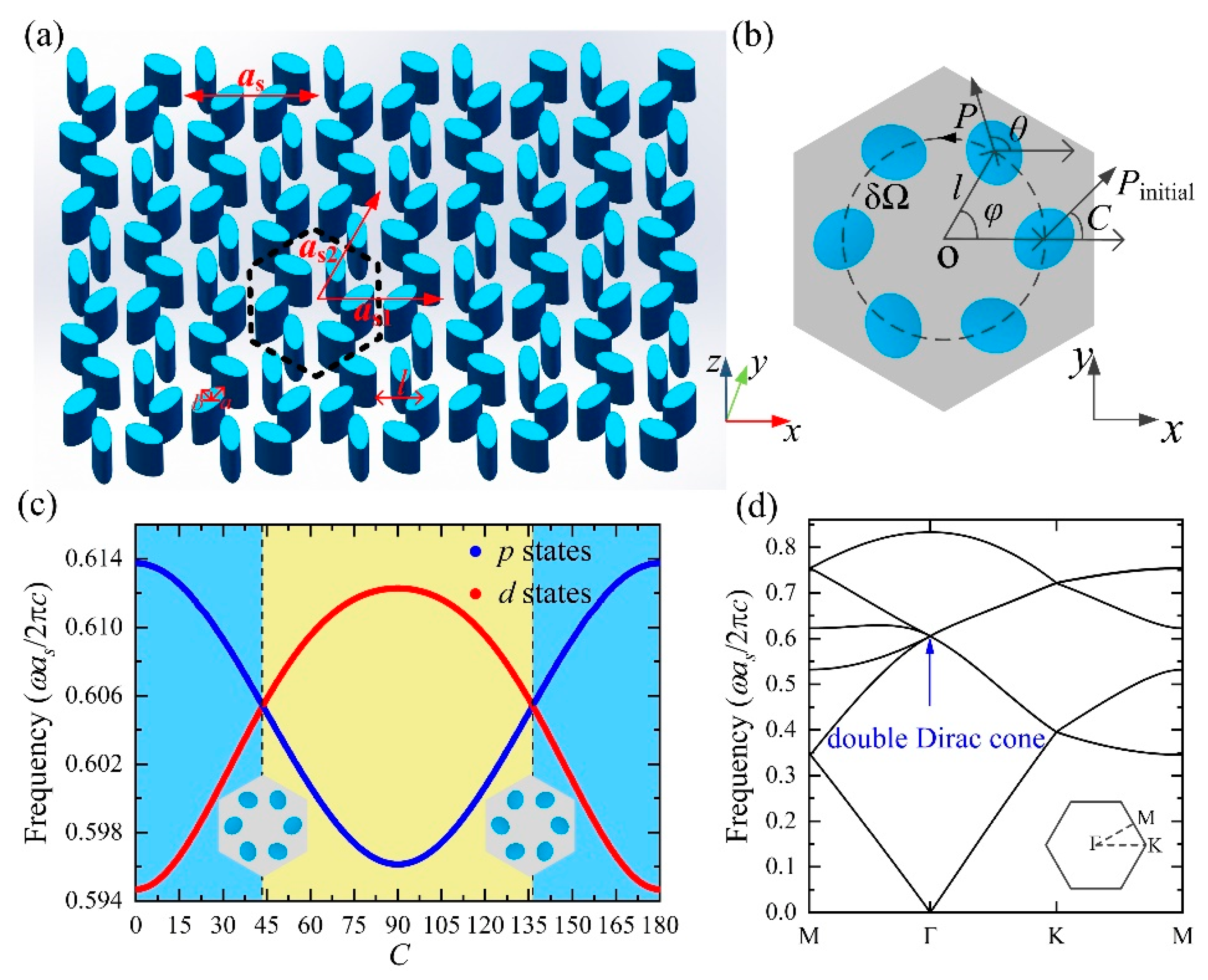
We start with a two-dimensional (2D) triangular lattice of elliptical alumina cylinders with relative permittivity and permeability immersed in an air host, as illustrated in Figure 1a. The distance between the centers of each cluster and each ellipse is , where is the lattice constant. The major axis of the elliptical cylinder is and the minor axis is . Here, we focus on the transverse magnetic (TM) mode of EM waves with out-of-plane electric field and in-plane magnetic field. According to the Maxwell equations, the propagation of time-harmonic TM waves in the PCs can be described by [30,31,37].
where is the speed of light and is the position-dependent relative permittivity. is the band index and is the Bloch function of the magnetic field at wavevector . By solving the generalized eigenvalue problem, we can obtain the dispersion relations between the eigenfrequency and the Bloch wavevector .
We then introduced a topological modification by rotating individual ellipses within a unit cell in different directions, while keeping the lattice intact. The theory of topological defects and homotopy theory [38,39,40] is adopted to describe the fundamental topological characteristic of the photonic crystal structure, shown in Figure 1b. Such a modification in the orientational order can be mapped on the order parameter space θ, and it is given as [38].
where denotes the polar angle of the center position of the ellipse in the polar coordinates , and C is the initial phase for . k is an integer or a half integer that represents the topological charge and is equal to the so called winding number n. It is determined by measuring the overall rotation in θ-space and is described by , where represents a closed contour. Owing to the symmetry of θ-space in the present photonic systems, n can take on the values of +1. Herein, corresponds to the vortex and hedgehog structure with the topological stability, which allows us to explore various topological states. Note that the elliptical scatterers are anisotropic and have the additional orientation degree of freedom, compared to the circular scatterers. Thus, the choice of the initial phase C enables the PCs to possess various symmetries, which can be leveraged to control the band gap closure and reopening, inducing multiple topological phase transitions. Based on tuning topological charge and initial phase C, this approach is more applicable to 2D dielectric PCs than conventional proposals [30,31,37], due to its high flexibility in the air background, which allows us to achieve structural reconfigurability in the microwave regime.
3. Results and Discussion
In this study, we revealed the topology of the modification structure with and observed multiple topological phase transitions in our system. Rather than refabricating the PCs to obtain topological orders of photonic states, the spatially inhomogeneous variations of the ellipse orientation within the unit cells could fine-tune the topological transition, where a continuous band gap closing and reopening was easily accomplished. Figure 1c provides the eigenfrequencies of the two twofold degenerated states at the Γ point, as a function of the initial phase C. We observed that the doubly degenerated band-edge eigenfrequencies changed smoothly and crossed with each other at and . It was shown that, other than the zone folding mechanism [37,41,42], the accidental quadruple Dirac degeneracy could be formed at the Brillouin zone center. The structural chirality was introduced by the rotation of the crystalline domains, while preserving the time-reversal symmetry, indicating that the corresponding band structures with and , were exactly the same, as displayed in Figure 1d. It is worth noting that the topological modifications of the crystalline domains and band inversion process induced by the spatial variation of the ellipse orientation were unique features in the topological photonic system, which ultimately led to the double topological phase transitions. In particular, when the order parameter maintained its rigidity and the dielectric pillars remained the C2 symmetry, the orientational modification was robust to realize the accidental Dirac degeneracy, on the triangular lattice. Such phenomena have not been found in previous studies on core-shell [30,31] or deformed-honeycomb [37,41,42] PCs for TM modes. Moreover, our approach enabled an easily tunable operation bandwidth and reconfigurable topological domain wall, with no need of changing the filling ratio or changing the position of the dielectric pillars, which was very useful in practical applications.
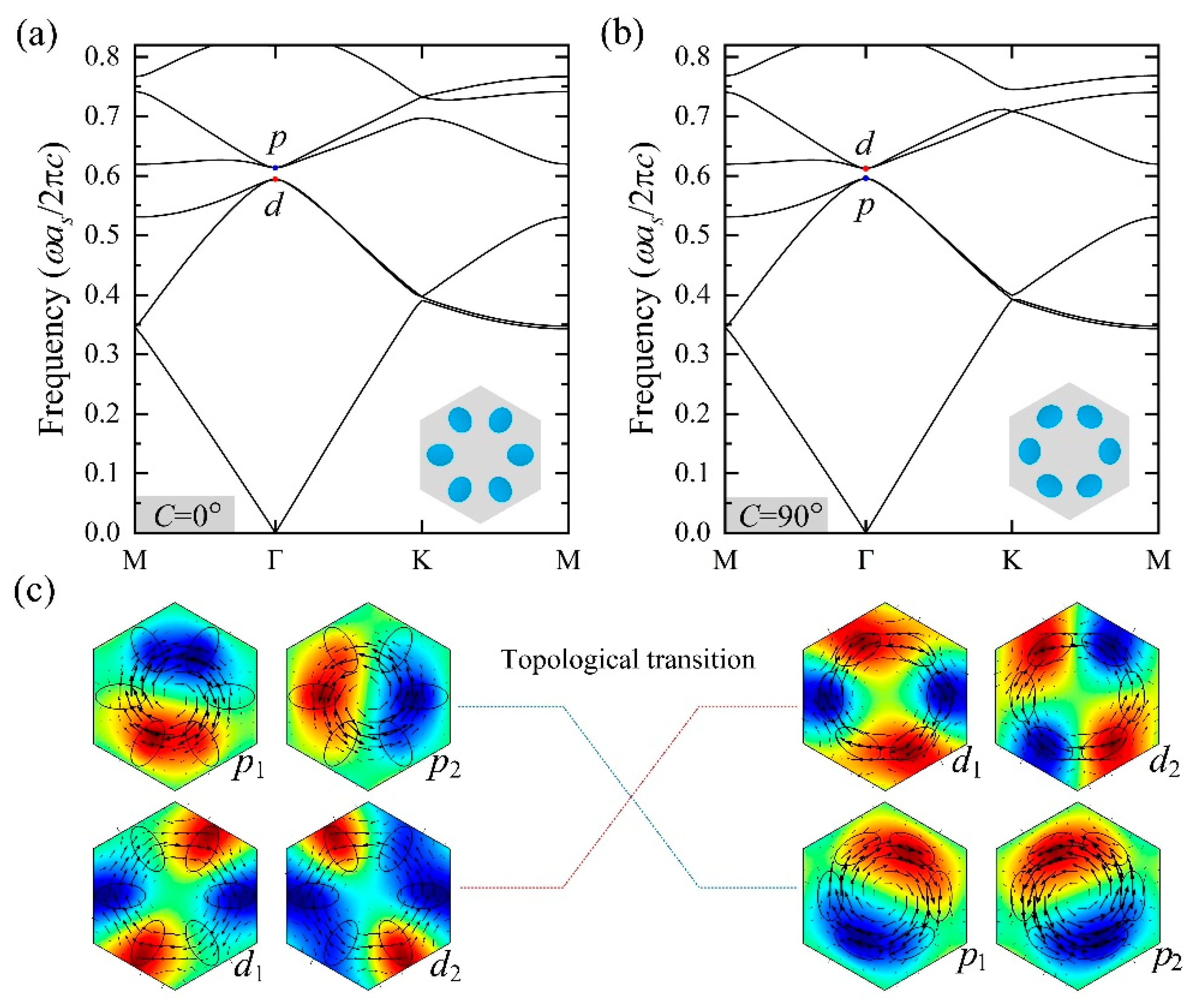
We then introduced a perturbation by varying the initial phase , which lifted the fourfold degeneracy at the Γ point and hence opened a complete band gap. Figure 2a,b show the corresponding dispersion relations of the TM modes for the radical configuration with and the azimuthal configuration with , respectively. The simulated electric field distributions of the degenerate dipolar (p-type) and quadrupolar (d-type) modes are illustrated in Figure 2c, which respectively correspond to the colored dots at the Γ point. The angular momenta of the wave function of electric fields and further construct the spin-1/2 for the pseudospin in the present PCs. In order to clarify the underlying physics of the pseudospin states, we plot the real-space distribution of the time-averaged Poynting vector around the Γ point, which expresses the energy flow in the radical and azimuthal configuration, as indicated by the black arrows. It can be seen that the rotation of the crystalline domains introduces the right- or left-hand circularly polarized chirality and all eigenstates display remarkable vortex features, encircling the center of the unit cell, which plays the role of the pseudospin degree of freedom. Instead of changing the lattice structure, it is shown how topological modes inversion between p-type and d-type states takes place under the spatial variation of the orientation of elliptical cylinders. For shown in Figure 2a, the p-type states are located on the upper side of the band gap, whereas the d-type states are located on the lower side, as per the analogy to electronic orbital shapes. For shown in Figure 2b, the degenerate states are flipped, i.e., the d-type states rise above p-type states, resulting in an inverted band structure and the topology of the band gap is different from the earlier case. To further reveal the topological property of the band gaps, we calculate the spin Chern numbers by employing the perturbation method [31,32,33,35], where the effective Hamiltonian of the photonic pseudospin Hall system, in the vicinity of the Γ point, shares a similar form with the Bernevig–Hughes–Zhang (BHZ) model for the Cd/Te/HgTe/CdTe quantum well system [4]. We find that the band gap has spin Chern numbers for the case of the radical configuration, hence, implying that it is a nontrivial band gap. Differently, the azimuthal configuration has the spin Chern numbers , which indicates the corresponding band gap is trivial in topology. The overall results, hence, confirm a topological transition from a nontrivial phase to a trivial phase in the present dielectric photonic systems.
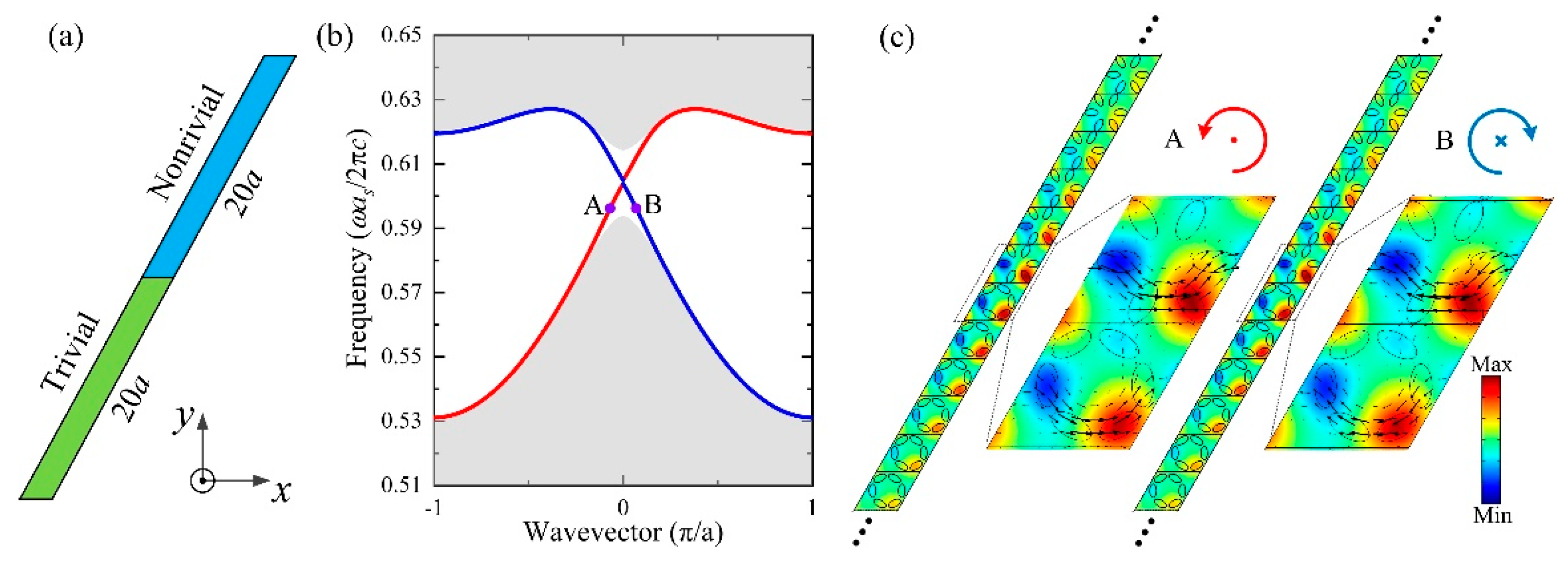
A fundamental evidence of the band topology is the appearance of topologically protected helical edge states at the interfaces between the two PCs, with different topological phases. As shown in Figure 3a,b, we calculated the projected band structure of a ribbon-shaped supercell composed of 20 unit cells of the topological nontrivial crystal and 20 unit cells of the trivial crystal. There appears to be a pair of additional edge states (represented by red and blue curves), within the overlapped bulk band gap of both crystals. The two edges states have opposite group velocities at a given frequency, indicating the existence of counter-propagations of the edge states. The real-space distributions of the electric field for the edge states, at points A and B, are plotted in Figure 3c, respectively, and both field maps indicate that the topologically protected edge states are confined at the interface of the supercell, and decay exponentially into the bulk. Further, the black arrows represent the time-averaged Poynting vectors and its anti-clockwise (clockwise) directions demonstrate the existence of the pseudospin-up (pseudospin-down) state, which unveils the pseudospin characteristics of these TM modes in the PCs. Note that, there is a tiny gap in the dispersions of the edge states, resulting from the breaking of the symmetry at the interface between the two PCs. However, the pseudospin is preserved and these modes can still be utilized to realize robust and backscattering-immune directional waveguides, as shown below.
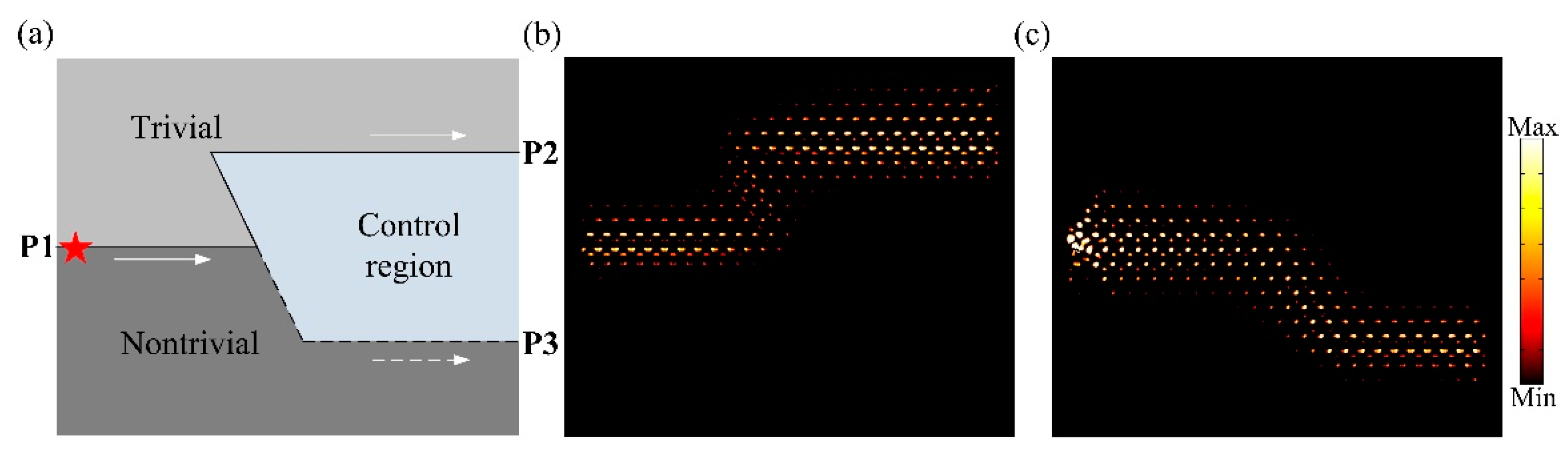
The structural reconfigurability is the cornerstone behind the current photonic functional devices and optical communication systems. To demonstrate the reconfigurability and capability of manipulating topologically protected edge states in our system, we designed topologically switchable waveguides at microwave frequencies, in which each elliptical rod attached to the pedestal was equipped with one computer-controlled motor, as shown in Figure 4a. The rotation orientation of the elliptical rods (highlighted in blue) was modified by a computer-controlled motorized stage. As a result, the topologically protected pathway could be automatically switched between two distinct topological configurations. Depending on the rotation angle selected, or , respectively, in the reconfigurable control region, the EM waves were transmitted either from Port 1 to Port 2, or from Port 1 to Port 3, as shown in Figure 4b,c. In addition, we stress that arbitrarily shaped interfaces could be created, based on the above controls, by tuning the configuration on both sides of the interface with distinct topological domains. In contrast to the conventional topological photonic systems, which are limited by fixed geometry or rely on the movement of the rods [28,30,31,35,37,41,42], this reconfigurable and flexible platform was highly desirable to realize the accurate control of unique device functionalities, by simply configuring the elliptical rods to any desired angle.
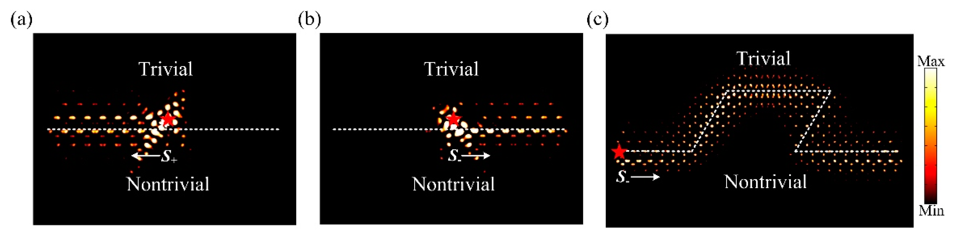
One of the most striking features of topological edge states is the topological protection from backscattering caused by defects and robust one-way propagation. Herein, we verified the helicity of the edge states in the topological photonic system, that is, the pseudospin degree of freedom controlled the direction of propagation. By selectively exciting the pseudospin-up (pseudospin-down) mode with the excitation source () of positive (negative) circular polarization, one-way propagation of the EM wave towards left and right directions, could be observed in Figure 5a,b, respectively. To further demonstrate the backscattering-immune property of these edge states, we introduced four sharp bends to the topological microwave channel as displayed in Figure 5c. When an EM wave was excited from a pseudospin-down source , it propagated along the trivial/nontrivial interface and could go around the structural bends without notable scattering losses. These results confirm the topological robustness of these edge states against certain defects and the inherently backscattering-immune one-way transport.
4. Conclusions
In summary, we have proposed a feasible scheme to realize the reconfigurable photonic topological insulator enabled by the photonic analog of QSHE, whose topological phase could be reconfigured by inhomogeneously tuning the orientation of elliptical cylinders within the unit cells. Our design principle and topological EM properties demonstrated here in the microwave frequency could be directly extended to near-infrared or even optical regimes to inspire many optical applications. Although our simulations focus on a specific type of topological charge , we believe that the mapping could realize diversified topological photonic phases with distinct characteristics, by varying the values of and . Thus, this flexible and versatile approach could be exploited to realize structural reconfigurability and adaptation to functional needs, via various θ-spaces, making it attractive for practical applications. The results open up new possibilities for free steering EM waves, along arbitrarily-shaped pathways, without any backscattering, which could be of immense value for future optical science and technology.
Author Contributions
Formal analysis, H.H.; Methodology, H.H.; Validation, S.H.; Supervision, J.C.; Writing—original draft, H.H.; Writing—review and editing, S.H. and J.C.
Funding
This work is supported by the National Science Foundation of China (Grant No.11374093); Young Scholar fund sponsored by common university and college of the province in Hunan.
Conflicts of Interest
The authors declare no conflict of interest.
References
- Tang, H.K.; Leaw, J.N.; Rodrigues, J.N.B.; Herbut, I.F.; Sengupta, P.; Assaad, F.F.; Adam, S. The role of electron-electron interactions in two-dimensional Dirac fermions. Science 2018, 361, 570–574. [Google Scholar] [CrossRef]
- Kane, C.L.; Mele, E.J. Quantum spin hall effect in graphene. Phys. Rev. Lett. 2005, 95, 226801. [Google Scholar] [CrossRef]
- Hasan, M.Z.; Kane, C.L. Colloquium: Topological insulators. Rev. Mod. Phys. 2010, 82, 3045. [Google Scholar] [CrossRef]
- Bernevig, B.A.; Hughes, T.L.; Zhang, S.C. Quantum spin Hall effect and topological phase transition in HgTe quantum wells. Science 2006, 314, 1757–1761. [Google Scholar] [CrossRef]
- He, C.; Ni, X.; Ge, H.; Sun, X.C.; Chen, Y.B.; Lu, M.H.; Liu, X.P.; Chen, Y.F. Acoustic topological insulator and robust one-way sound transport. Nat. Phys. 2016, 12, 1124–1129. [Google Scholar] [CrossRef] [Green Version]
- Zhang, Z.; Wei, Q.; Cheng, Y.; Zhang, T.; Wu, D.; Liu, X. Topological creation of acoustic pseudospin multipoles in a flow-free symmetry-broken metamaterial lattice. Phys. Rev. Lett. 2017, 118, 084303. [Google Scholar] [CrossRef]
- Lu, J.-Y.; Qiu, C.; Ye, L.; Fan, X.; Ke, M.; Zhang, F.; Liu, Z. Observation of topological valley transport of sound in sonic crystals. Nat. Phys. 2017, 13, 369–374. [Google Scholar] [CrossRef]
- Mousavi, S.H.; Khanikaev, A.B.; Wang, Z. Topologically protected elastic waves in phononic metamaterials. Nat. Commun. 2015, 6, 8682. [Google Scholar] [CrossRef] [Green Version]
- Huang, H.B.; Chen, J.J.; Huo, S.Y. Simultaneous topological Bragg and locally resonant edge modes of shear horizontal guided wave in one-dimensional structure. J. Phys. D: Appl. Phys. 2017, 50, 275102. [Google Scholar] [CrossRef]
- Chen, J.J.; Huang, H.B.; Huo, S.Y.; Tan, Z.H.; Xie, X.P.; Cheng, J.C.; Huang, G.L. Self-ordering induces multiple topological transitions for in-plane bulk waves in solid phononic crystals. Phys. Rev. B 2018, 98, 014302. [Google Scholar] [CrossRef]
- Harari, G.; Bandres, M.A.; Lumer, Y.; Rechtsman, M.C.; Chong, Y.D.; Khajavikhan, M.; Christodoulides, D.N.; Segev, M. Topological insulator laser: Theory. Science 2018, 359, 1230. [Google Scholar] [CrossRef]
- Bandres, M.A.; Wittek, S.; Harari, G.; Parto, M.; Ren, J.; Segev, M.; Christodoulides, D.N.; Khajavikhan, M. Topological insulator laser: Experiments. Science 2018, 359, 1231. [Google Scholar] [CrossRef]
- Lustig, E.; Weimann, S.; Plotnik, Y.; Lumer, Y.; Bandres, M.A.; Szameit, A.; Segev, M. Photonic topological insulator in synthetic dimensions. Nature 2019, 567, 356. [Google Scholar] [CrossRef]
- Yang, Y.; Gao, Z.; Xue, H.; Zhang, L.; He, M.; Yang, Z.; Singh, R.; Chong, Y.; Zhang, B.; Chen, H. Realization of a three-dimensional photonic topological insulator. Nature 2019, 565, 622. [Google Scholar] [CrossRef]
- Xie, B.Y.; Wang, H.F.; Wang, H.X.; Zhu, X.Y.; Jiang, J.H.; Lu, M.H.; Chen, Y.F. Second-order photonic topological insulator with corner states. Phys. Rev. B 2018, 98, 205147. [Google Scholar] [CrossRef]
- Haldane, F.D.M.; Raghu, S. Possible realization of directional optical waveguides in photonic crystals with broken time-reversal symmetry. Phys. Rev. Lett. 2008, 100, 013904. [Google Scholar] [CrossRef]
- Raghu, S.; Haldane, F.D.M. Analogs of quantum-Hall-effect edge states in photonic crystals. Phys. Rev. A 2008, 78, 033834. [Google Scholar] [CrossRef]
- Wang, Z.; Chong, Y.D.; Joannopoulos, J.D.; Soljăcić, M. Reflection-free one-way edge modes in a gyromagnetic photonic crystal. Phys. Rev. Lett. 2008, 100, 013905. [Google Scholar] [CrossRef]
- Wang, Z.; Chong, Y.; Joannopoulos, J.D.; Soljăcić, M. Observation of unidirectional backscattering-immune topological electromagnetic states. Nature 2009, 461, 772–775. [Google Scholar] [CrossRef] [Green Version]
- Poo, Y.; Wu, R.-X.; Lin, Z.; Yang, Y.; Chan, C.T. Experimental realization of self-guiding unidirectional electromagnetic edge states. Phys. Rev. Lett. 2011, 106, 093903. [Google Scholar] [CrossRef]
- Hafezi, M.; Demler, E.A.; Lukin, M.D.; Taylor, J.M. Robust optical delay lines with topological protection. Nat. Phys. 2011, 7, 907–912. [Google Scholar] [CrossRef] [Green Version]
- Hafezi, M.; Mittal, S.; Fan, J.; Migdall, A.; Taylor, J.M. Imaging topological edge states in silicon photonics. Nat. Photon. 2013, 7, 1001–1005. [Google Scholar] [CrossRef] [Green Version]
- Fang, K.; Yu, Z.; Fan, S. Realizing effective magnetic field for photons by controlling the phase of dynamic modulation. Nat. Photon. 2012, 6, 782–787. [Google Scholar] [CrossRef]
- Umucalılar, R.O.; Carusotto, I. Artificial gauge field for photons in coupled cavity arrays. Phys. Rev. A 2011, 84, 043804. [Google Scholar] [CrossRef]
- Fang, K.; Yu, Z.; Fan, S. Microscopic theory of photonic one-way edge mode. Phys. Rev. B 2011, 84, 075477. [Google Scholar] [CrossRef]
- Ma, T.; Khanikaev, A.B.; Mousavi, S.H.; Shvets, G. Guiding Electromagnetic Waves around Sharp Corners: Topologically Protected Photonic Transport in Metawaveguides. Phys. Rev. Lett. 2015, 114, 127401. [Google Scholar] [CrossRef]
- Chen, W.J.; Jiang, S.J.; Chen, X.D.; Zhu, B.; Zhou, L.; Dong, J.W.; Chan, C.T. Experimental realization of photonic topological insulator in a uniaxial metacrystal waveguide. Nat. Commun. 2014, 5, 5782. [Google Scholar] [CrossRef] [Green Version]
- Barik, S.; Miyake, H.; DeGottardi, W.; Waks, E.; Hafezi, M. Two-dimensionally confined topological edge states in photonic crystals. New J. Phys. 2016, 18, 113013. [Google Scholar] [CrossRef] [Green Version]
- Ma, T.X.; Wang, Y.S.; Zhang, C. Photonic and phononic surface and edge modes in three-dimensional phoxonic crystals. Phys. Rev. B 2018, 97, 134302. [Google Scholar] [CrossRef]
- Li, Y.; Mei, J. Double Dirac cones in two-dimensional dielectric photonic crystals. Opt. Express 2015, 23, 12089–12099. [Google Scholar] [CrossRef]
- Xu, L.; Wang, H.X.; Xu, Y.D.; Chen, H.Y.; Jiang, J.H. Accidental degeneracy in photonic bands and topological phase transitions in two-dimensional core-shell dielectric photonic crystals. Opt. Express 2016, 24, 18059–18071. [Google Scholar] [CrossRef]
- Fang, K.; Fan, S. Controlling the flow of light using the inhomogeneous effective gauge field that emerges from dynamic modulation. Phys. Rev. Lett. 2013, 111, 203901. [Google Scholar] [CrossRef]
- Reiskarimian, N.; Krishnaswamy, H. Magnetic-free non-reciprocity based on staggered commutation. Nat. Commun. 2016, 7, 11217. [Google Scholar] [CrossRef] [Green Version]
- Rechtsman, M.C.; Zeuner, J.M.; Plotnik, Y.; Lumer, Y.; Podolsky, D.; Dreisow, F.; Nolte, S.; Segev, M.; Szameit, A. Photonic floquet topological insulators. Nature 2013, 496, 196. [Google Scholar] [CrossRef]
- Cheng, X.; Jouvaud, C.; Ni, X.; Mousavi, S.H.; Genack, A.Z.; Khanikaev, A.B. Robust reconfigurable electromagnetic pathways within a photonic topological insulator. Nat. Mater. 2016, 15, 542. [Google Scholar] [CrossRef]
- Shalaev, M.I.; Desnavi, S.; Walasik, W.; Litchinitser, N.M. Reconfigurable topological photonic crystal. New J. Phys. 2018, 20, 023040. [Google Scholar] [CrossRef] [Green Version]
- Wu, L.-H.; Hu, X. Scheme for achieving a topological photonic crystal by using dielectric material. Phys. Rev. Lett. 2015, 114, 223901. [Google Scholar] [CrossRef]
- Mermin, N.D. The topological theory of defects in ordered media. Rev. Mod. Phys. 1979, 51, 591. [Google Scholar] [CrossRef]
- Kleman, M.; Lavrentovich, O.D. Soft Matter Physics: An Introduction; Springer: New York, NY, USA, 2003. [Google Scholar]
- Podgornik, R. Principles of condensed matter physics. J. Stat. Phys. 1996, 83, 1263–1265. [Google Scholar] [CrossRef]
- Yves, S.; Fleury, R.; Berthelot, T.; Fink, M.; Lemoult, F.; Lerosey, G. Crystalline metamaterials for topological properties at subwavelength scales. Nat. Commun. 2017, 8, 16023. [Google Scholar] [CrossRef] [Green Version]
- Yang, Y.; Xu, Y.F.; Xu, T.; Wang, H.X.; Jiang, J.H.; Hu, X.; Hang, Z.H. Visualization of a unidirectional electromagnetic waveguide using topological photonic crystals made of dielectric materials. Phys. Rev. Lett. 2018, 120, 217401. [Google Scholar] [CrossRef]
Figure 1.
(a) Schematic of triangular-lattice photonic crystals (PCs), consisting of six elliptical alumina cylinders (blue) embedded in air background (gray). (b) Top-view unit cell and θ-space of the PCs. (c) Calculated eigenfrequencies of the two two-fold degenerated states at the Γ point, in dependence to the initial phase C. Unit cells of the topological transition points are indicated in the inset. The band inversion effect and multiple topological transitions was clearly observed. The cyan (yellow) regions represent the nontrivial (trivial) regimes. (d) Dispersion relations of the structures in which and . A double Dirac cone with a four-fold accidental degeneracy is seen at the Γ point. Inset: First Brillouin zone of triangular lattice.

Figure 2.
Band structures and topological modes inversion of the PCs. Corresponding unit cells are displayed at the bottom right corner in each subgraph. (a) The radical configuration with leading to topologically nontrivial bandgap with p-type states having a higher frequency than the d-type states. (b) The azimuthal configuration with , leading to topologically trivial bandgap with the p- and d-type states inverted. (c) The electric field distributions of the p/d eigenstates at the Γ point. The black arrows represent the time-averaged Poynting vector around the Γ point.

Figure 3.
(a) Schematic of a ribbon-shaped supercell consisting of 20 radical configuration and 20 azimuthal configuration for the nontrivial and trivial regions, respectively. (b) Calculated band structure of the supercell, where periodic (absorbing) boundary conditions were imposed on the right and left (top and bottom) boundaries, respectively. The red (blue) curve represents the pseudospin-up (pseudospin-down) edge state, whereas the shadow regions indicate the bulk photonic bands. (c) The corresponding electric field distribution of the edge states localized at the interface of the supercell corresponding to the points A and B in (b). Black arrows represent the time-averaged Poynting vector.

Figure 4.
(a) Schematic diagram of the reconfigurable topological switch. The pedestals of the elliptical rods in the blue region are attached to computer-controlled motors by which the elliptical rods could be rotated to different angles. (b,c) Electric field intensity distributions when switched between the different topological states. The electromagnetic (EM) waves transmitted through port 2 (or port 3) at the rotation angle of the reconfigurable control region (highlighted in blue, in (a)). Perfectly matched layers were imposed to the surrounds of the whole PC structures to absorb output wave.

Figure 5.
(a,b) Simulated electric field maps for one-way edge state excited with a positively and negatively circularly polarized dipole show unidirectional propagation towards left and right directions, respectively. (c) Electric field maps of robust one-way edge states along interfaces with sharp tuning angles show that the EM waves can transmit around defects without backscattering. Perfectly matched layers are imposed to the surrounds of the whole PC structures to absorb output waves.

© 2019 by the authors. Licensee MDPI, Basel, Switzerland. This article is an open access article distributed under the terms and conditions of the Creative Commons Attribution (CC BY) license (http://creativecommons.org/licenses/by/4.0/).
Share and Cite
MDPI and ACS Style
Huang, H.; Huo, S.; Chen, J. Reconfigurable Topological Phases in Two-Dimensional Dielectric Photonic Crystals. Crystals 2019, 9, 221. https://0-doi-org.brum.beds.ac.uk/10.3390/cryst9040221
AMA Style
Huang H, Huo S, Chen J. Reconfigurable Topological Phases in Two-Dimensional Dielectric Photonic Crystals. Crystals. 2019; 9(4):221. https://0-doi-org.brum.beds.ac.uk/10.3390/cryst9040221
Chicago/Turabian StyleHuang, Hongbo, Shaoyong Huo, and Jiujiu Chen. 2019. "Reconfigurable Topological Phases in Two-Dimensional Dielectric Photonic Crystals" Crystals 9, no. 4: 221. https://0-doi-org.brum.beds.ac.uk/10.3390/cryst9040221
Note that from the first issue of 2016, this journal uses article numbers instead of page numbers. See further details here.