Silicon Heterojunction Solar Cells with p-Type Silicon Carbon Window Layer
by
Chia-Hsun Hsu
1, 
Xiao-Ying Zhang
1,
Ming Jie Zhao
1,
Hai-Jun Lin
1,
Wen-Zhang Zhu
1 and
Shui-Yang Lien
1,2,* 1
School of Opto-electronic and Communication Engineering, Xiamen University of Technology, Xiamen 361024, China
2
Department of Materials Science and Engineering, Da-Yeh University, Chunghwa 51591, Taiwan
*
Author to whom correspondence should be addressed.
Crystals 2019, 9(8), 402; https://0-doi-org.brum.beds.ac.uk/10.3390/cryst9080402
Submission received: 31 May 2019
/
Revised: 30 July 2019
/
Accepted: 31 July 2019
/
Published: 3 August 2019
(This article belongs to the Special Issue Selected Papers from Taiwan Association for Academic Innovation, TAAI 2019)
Abstract
:Boron-doped hydrogenated amorphous silicon carbide (a-SiC:H) thin films are deposited using high frequency 27.12 MHz plasma enhanced chemical vapor deposition system as a window layer of silicon heterojunction (SHJ) solar cells. The CH4 gas flow rate is varied to deposit various a-SiC:H films, and the optical and electrical properties are investigated. The experimental results show that at the CH4 flow rate of 40 sccm the a-SiC:H has a high band gap of 2.1 eV and reduced absorption coefficients in the whole wavelength region, but the electrical conductivity deteriorates. The technology computer aided design simulation for SHJ devices reveal the band discontinuity at i/p interface when the a-SiC:H films are used. For fabricated SHJ solar cell performance, the highest conversion efficiency of 22.14%, which is 0.33% abs higher than that of conventional hydrogenated amorphous silicon window layer, can be obtained when the intermediate band gap (2 eV) a-SiC:H window layer is used.
1. Introduction
Solar energy is on the edge of becoming one of the main energy sources, and crystalline silicon (c-Si) solar cells are currently a dominant product in the photovoltaic market. Due to the increasing cost of processed crystalline silicon ingots over the past years, the silicon wafer thickness has been demanded to decrease for solar cell fabrication. This trend was stopped due to the bending of thin wafers during high temperature processing of standard c-Si solar cells, and thus results in lots of efforts focusing on technologies for low material usage. Amorphous–crystalline silicon heterojunction (SHJ) solar cells are a hot topic because of their lower processing temperature (below 250 °C) and a higher open-circuit voltage (Voc) in comparison to homojunction c-Si devices. A high conversion efficiency of over 26% of SHJ solar cells has been achieved [1]. The SHJ solar cells use a c-Si absorber while the other components have a thin-film structure. An intrinsic hydrogenated amorphous silicon (a-Si:H) provides excellent passivation of c-Si surface and carrier selectivity [2,3]. Unlike the homojunction c-Si cells with metals directly contacting to absorber, in SHJ the recombination-active contacts are replaced by passivated contacts, where semiconductor layers are between absorber and metal. Therefore, SHJ cells have a high Voc of larger than 720–740 mV [4,5,6]. The thin-film components are deposited using plasma enhanced chemical vapor deposition (PECVD), which is a widely accepted technique for thin-film production. The primary reason for its acceptance is its capability to operate at lower temperatures than thermally driven CVD. In PECVD a plasma is usually ignited and sustained by applying a high frequency voltage to a low-pressure gas, leading to inelastic collisions between electrons and gas molecules forming highly reactive species without significantly raising the gas temperature. A well-known loss of SHJ solar cells is parasitic absorption loss of blue light of a-Si:H layers on the light-entering side [7,8,9]. The ideal thin film for a window layer of SHJ solar cells should have low light absorption, low resistivity, and high conductivity. Several strategies are being designated to help solve this problem such as wider/indirect band gap materials, thinner layers or interdigitated back contact solar cells [8,9,10,11,12,13]. Incorporating carbon or oxygen into a-Si:H matrix widens the band gap in a range between 1.7 to 2.7 eV [14,15], reducing the absorption coefficient and parasitic absorption for a given layer thickness. For an a-SiC:H film with a band gap of the photoconductivity and dark conductivity 1.8–2 eV, the photoconductivity and photosensitivity are 10−4 S/cm and 106, respectively. The photoconductivity of a-SiC:H with a band gap above 2.2 eV degrades to about 10−10 S/cm. Although properties of a-SiC:H have been widely studied, the effect of the films on performance of SHJ solar cells is not fully understood.
In this study, different p-type a-SiC:H films are prepared by high frequency 27.12 MHz PECVD. The gas flow rate of CH4 is varied to obtain a-SiC:H films with different band gap, photoconductivity, dark conductivity, and atomic composition. The transmittance and absorption spectra of the p-type a-SiC:H films were measured by a UV-visible spectrometer. The band gap of the films was estimated by Tauc plot with the equation:
where α is the absorption coefficient, hv is the incident light energy, A is a proportion constant, and Eg is the band gap. The value of exponent n determines the nature of electronic transition. For direct transition, n = 1/2 and for indirect transition, n = 2. The dark conductivity of the films was measured at room temperature using a source-measure unit (Keithley 2400). The photoconductivity of the films was obtained by a solar simulator under AM1.5G (100 mW/cm2). The atomic ratio of the films were measured by an X-ray photoelectron spectroscopy (XPS). The current density-voltage (J-V) curves and external quantum efficiency (EQE) of the SHJ solar cells with different p-type layer were measured under AM1.5G conditions by a solar simulator consisting of xenon lamp and halogen lamp.
2. Experimental
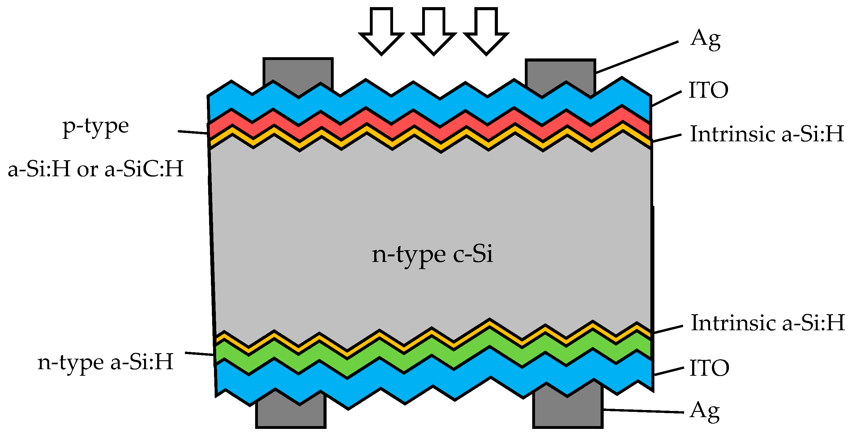
Boron-doped a-SiC:H film films were prepared by using 27.12 MHz plasma enhanced chemical vapor deposition (PECVD) with a gas mixture of SiH4, H2, B2H6 and CH4 on glasses and silicon wafers. The glasses were cleaned with deionized water, acetone, alcohol, and deionized water in sequence at room temperature. The wafers were cleaned by standard Radio Corporation of America process (RCA) processes, followed by a dip in 2% hydrogen fluoride. Then, the substrates were blow-dried by nitrogen gas. During a-SiC:H deposition, the substrate temperature was 250 °C, and the pressure was 0.6 Torr. The CH4 gas flow rate was varied from 0 to 50 sccm. The H2 flow rate was changed from 90 to 40 sccm to keep the total flow rate of (CH4+H2) at 90 sccm. Detailed deposition parameters are summarized in Table 1. For SHJ solar cell fabrication, the scheme of the device structure is shown in Figure 1. N-type n-type c-Si wafers (2 × 2 cm2) with resistivity of 0.5 Ω-cm and thickness of 100 μm were used as an absorber layer. The wafers were textured by solutions containing NaOH (2 wt%) and isopropyl alcohol (4 vol%) for 25 min to produce random pyramidal surfaces. Then, the wafers were cleaned by RCA process, and transferred to a vacuum chamber. A 5 nm-thick intrinsic a-Si:H layer was deposited on the both sides of the wafer to passivate dangling bonds on the wafer surfaces. Different p-type a-SiC:H films were then deposited on the wafer front side, and a n-type a-Si:H layer was deposited on the wafer rear side. The intrinsic, p-type and n-type layers were deposited by PECVD at 250 °C. An indium tin oxide (ITO) with a thickness of 80 nm and metal grids were deposited on both sides by radio-frequency magnetron sputtering at room temperature. The surface texturing and ITO was used for minimizing the front surface reflection. Cell fabrication was finished with thermally evaporated silver metal grid electrodes on the both sides of the wafer.
3. Results
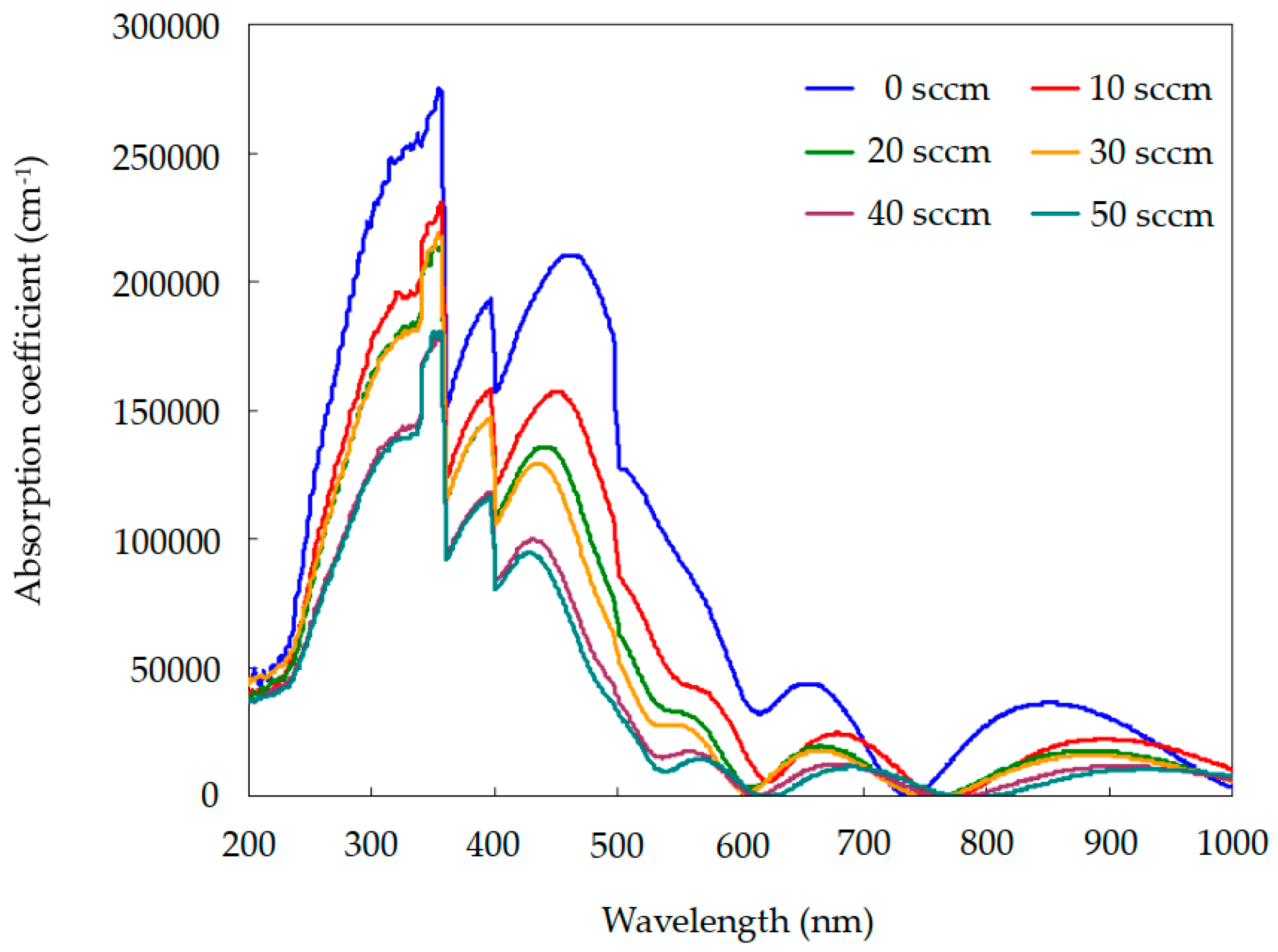
A window layer with a low light absorption is very important for SHJ solar cells as it in turn means that more light can be absorbed in the absorber layer. Moreover, light absorbed in the window layer would not contribute to device current density. The optical absorption coefficient, α, is evaluated using transmittance and reflectance spectra according to the equation:
where d is the film thickness, T is the transmittance, and R is the reflectance. The thickness of the thin films increases with increasing the CH4 gas flow rate. However, in this study, the thickness is kept to 15 nm for all the p-type layers. Figure 2 shows the absorption coefficient of a-SiC:H deposited with different H2/CH4 gas ratio in the wavelength range of 200–1000 nm. Without CH4 gas, the film is a-Si:H and the absorption coefficient is the largest over the whole investigated wavelength region. The absorption coefficient decreases when the CH4 flow rate increases. This might be due to the increase of the incorporation of C into a-Si:H network, leading to reduction in absorption coefficient. For c-Si solar cells having the strongest absorption, around 600 nm wavelength, the absorption coefficient at this wavelength (α600) can be used for comparison. The value of α600 is about 4.5 × 104 cm−1 at the CH4 flow rate of 0. When the gas flow rate larger than 10 sccm, α600 decreases to below 104 cm−1, which is the least requirement for a window layer of silicon-based solar cells.
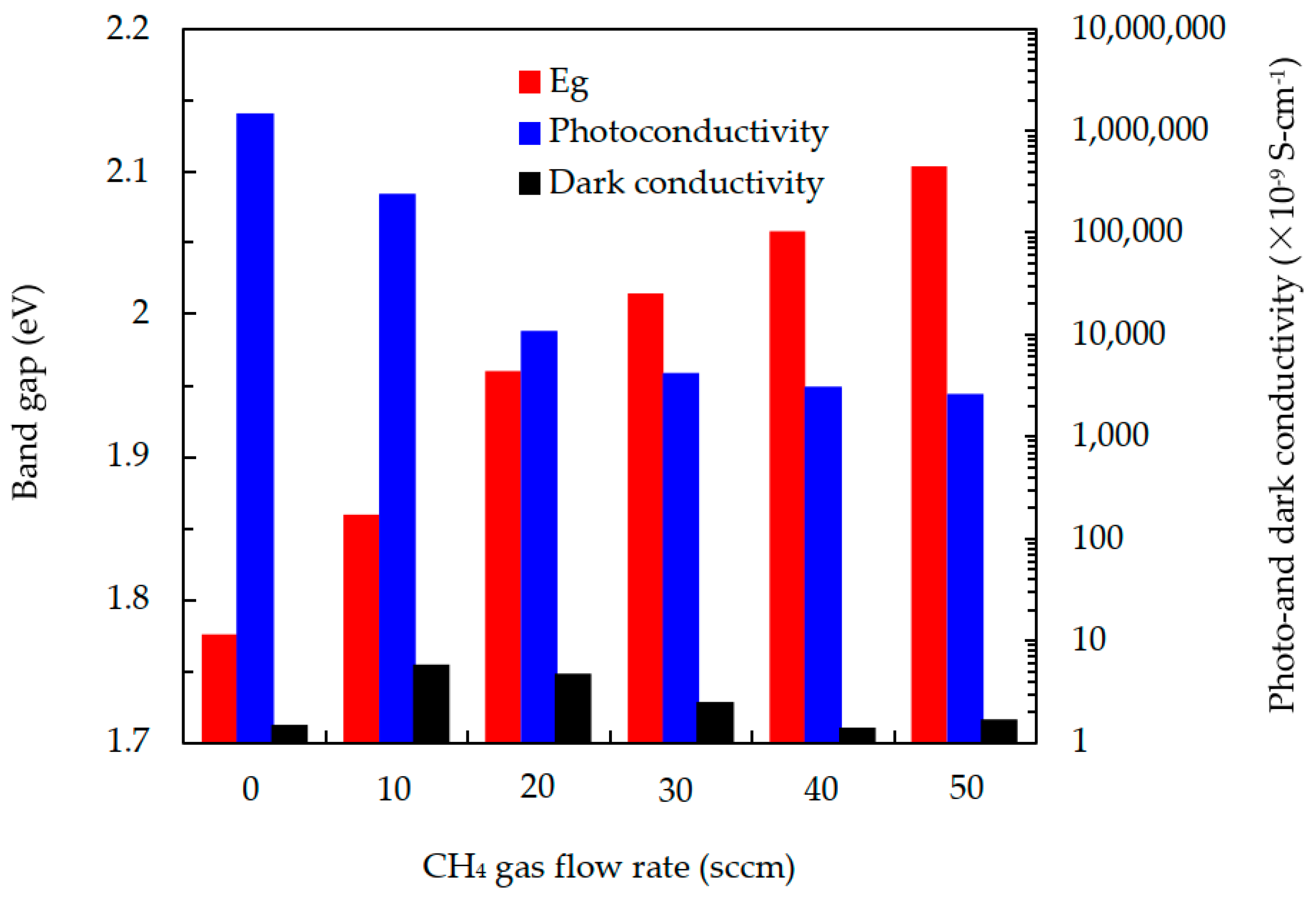
Figure 3 shows the optical band gap, photoconductivity and dark conductivity of the a-Si:H films as a function of CH4 gas flow rate. At CH4 gas flow rate of 0, the deposited film has a band gap of 1.78 eV, which is a typical value of a-Si:H. The band gap significantly increases from 1.86 to 2.11 eV when the CH4 gas flow rate increases from 10 to 50 sccm. The increased band gap results from the incorporation of C into the films. The higher band gap indicates that a cut-off wavelength would shift toward lower wavelength region and the film is relatively more transparent to light. The increased CH4 flow rate could enhance the dissociation of the CH4 and SiH4 molecules during PECVD deposition process. This leads to more Si-C bonds in the deposited films. However, it should be noted that carbon incorporation into a-Si:H would induce more structural disorder and defects, deteriorating electrical properties of the films. It has been reported that the paramagnetic defects in a-SiC:H films are mainly related with carbon incorporation, which leads to development of structural disorder, i.e., homonuclear interatomic bonds (Si-Si, C-C) [16,17,18]. In a mixed sp2- and sp3-coordinated disordered carbon network, the possible types of paramagnetic defects can be dangling σ-bonds and unpaired π-electrons associated with a single sp2-coordinated carbon atom and a carbon cluster with an odd number of sp2-sites [19]. The photoconductivity is 1.5 × 10⁻³ S/cm for a-Si:H (CH4 flow rate = 0), and it decrease significantly to 2.6 × 10⁻⁶ S/cm when the CH4 flow rate increases to 50 sccm. The dark conductivity shows a smaller influence by the CH4 flow rate, and ranges from 1 to 6 × 10⁻⁹ S/cm. Therefore, there is a tradeoff between the gain in band gap and the loss in electrical properties at increasing CH4 flow rate.
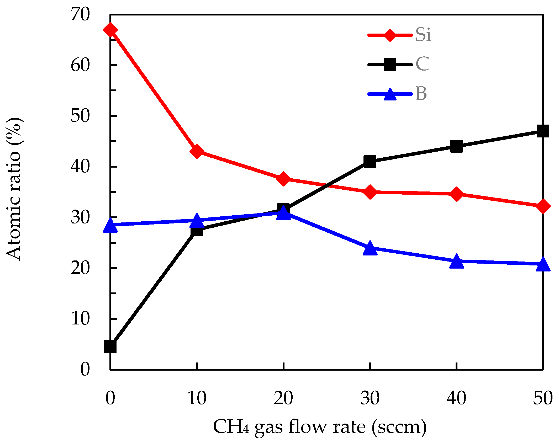
Figure 4 shows the Si, C and B elemental ratio measured by XPS. For the film deposited without CH4, the carbon atomic ratio is as low as 4.5%, the silicon ratio is about 67%, and boron ratio is around 28.5%. The little carbon content is due to the contamination from environment as the carbon gas was not used during deposition. The increase in the CH4 flow rate from 10 to 50 sccm, the carbon atomic ratio obviously increases from 27% to 45%, while the silicon and boron contents decrease. The boron content is in a range of 28.5% to 30.9% but decreases to 20.8% to 24% when the CH4 flow rate increases to 30–50 sccm. The incorporation of the carbon atoms into the films increases as the CH4 gas flow rate increases. The carbon atoms could replace the silicon or boron atoms sites. The boron content thus decreases with increasing the CH4 flow rate. This indicates that the increase in carbon content to certain level (in this case larger than silicon content) decreases doping efficiency of boron to the films. The boron is used as a dopant for creating p-type silicon thin-film layer. As the CH4 flow rate increases, the carbon content of the films increases, but the boron content decreases. The dark conductivity of the films thus decreases with increasing the CH4 flow rate.
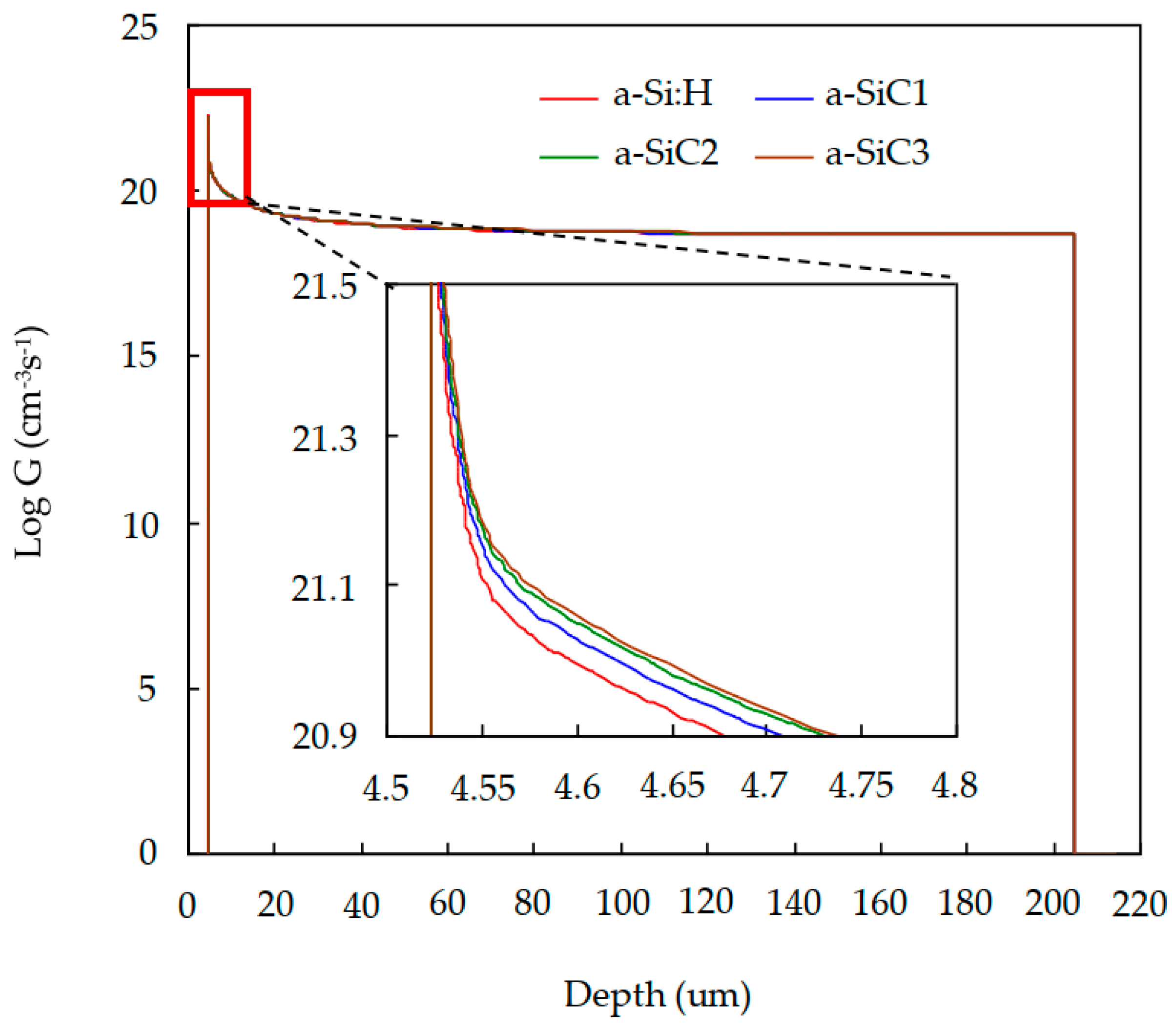
To gain an insight of the SHJ with different a-SiC:H window layers, the film properties are input into technology computer aided design (TCAD) simulation software. The device structure and parameters can be found elsewhere [20,21]. The a-SiC:H films with band gaps of 1.78 (a-Si:H), 1.85 (a-SiC1), 2 (a-SiC2) and 2.1 eV (a-SiC3) are used, corresponding to CH4 gas flow rates of 0, 10, 30 and 50 sccm, respectively. The detailed deposition parameters of the a-Si:H, a-SiC1, a-SiC2, a-SiC3 films are listed in Table 2. Figure 5 shows the photogeneration rate (G) in logarithm versus the device depth for the SHJ cells with different a-SiC:H window layer. The light enters into the device from the p-type layer side. The depth indicates the distance from the front surface of the devices. In general, the highest photogeneration rate is at the surface of the light entering side, and then exponentially decreases as the depth increases. A close view of the surface is shown in the inset of Figure 5. It is clearly seen that a-Si:H window layer has the lowest photogeneration rate. The a-SiC1 with the band gap of 1.85 eV leads to an increased generation rate. The generation rate further increases when a-SiC2 and a-SiC3 are used, but the difference between these two curves is less significant. This infers that the gain in photocurrent due to the increased band gap would saturate when band gap reaches 2 eV.
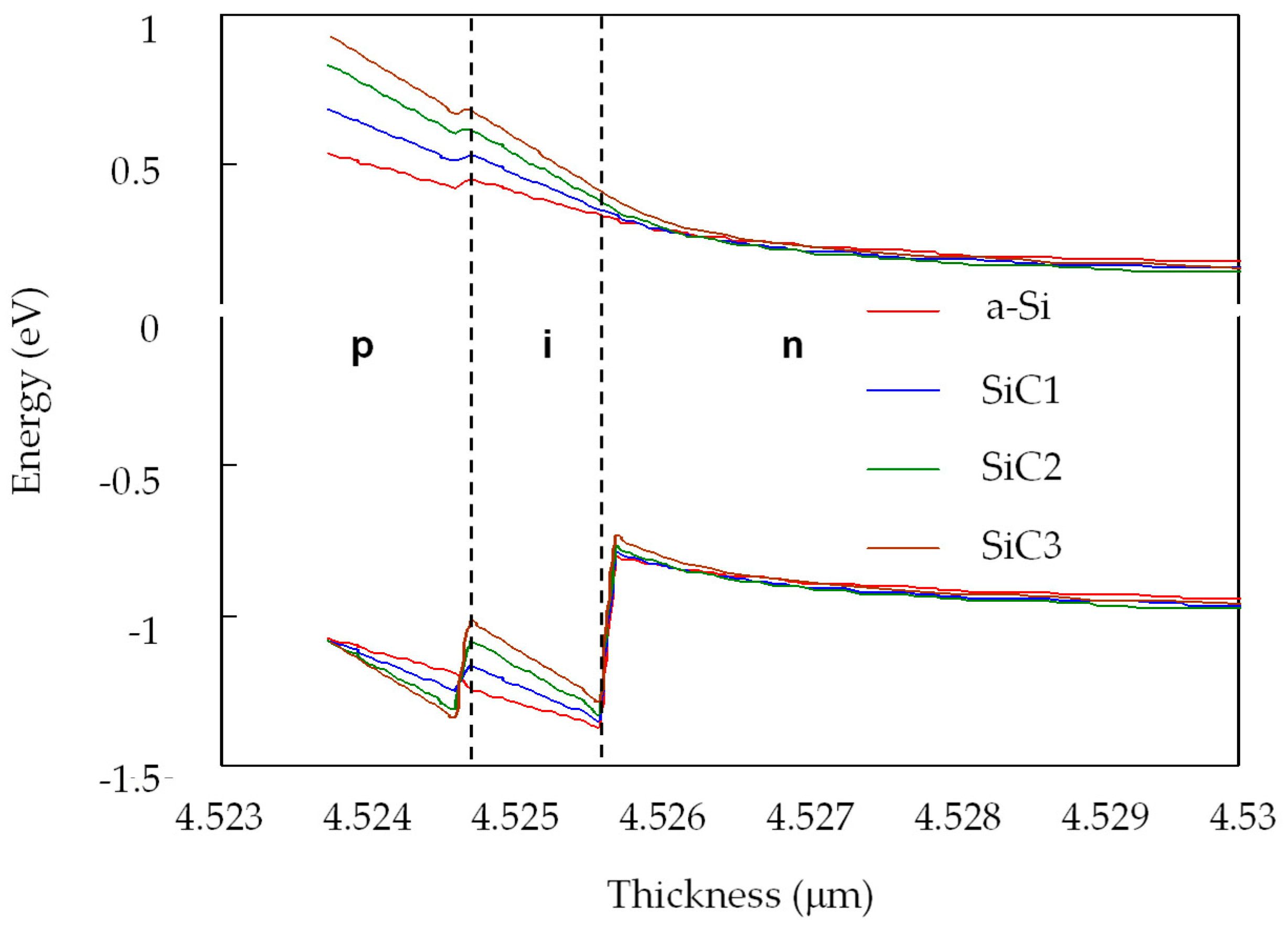
Figure 6 shows the simulated band structure of the SHJ solar cells with p-type a-Si:H, a-SiC1, a-SiC2, and a-SiC3 window layers. In the TCAD simulation, the doping concentration of the p-type a-Si:H and a-SiC was 1019 cm−3. The values of the electron affinity for the p-type a-Si:H and a-SiC were set to 4 and 3.9 eV, respectively [22,23]. The work function values of the p-type a-Si:H layer and a-SiC layers were calculated to be 5.33 and 5.43 eV, respectively, which were in the range of literature values [24,25]. It can be seen that the carrier selectivity of the SHJ solar cells, in which electrons move toward n-side as there is a barrier at front i/n region and holes toward p-side by tunneling. It is reported that for n-type SHJ solar cells, valence band offset at front amorphous/crystalline silicon interface is more crucial than conduction band offset [26]. Consider the p-type a-Si:H layer, the valence band offset (typically about 0.45–0.55 eV) occurs at i/n interface, and this region cause hole accumulation, leading to an minority carrier inversion layer near the n-type c-Si surface. This inversion layer is known to play important role of reducing recombination rate of c-Si interface [27]. As the i-layer is very thin, which is 1 nm in this simulation and is less than 5 nm for actual devices, the holes can tunnel through the valence band barrier. The replacement of the p-type a-Si:H with a-SiC:H leads more bend bending, which is favor for increasing build-in potential and Voc. However, it is observed that a discontinuity occurs at p/i interface. It has been reported that for SHJ solar cells, discontinuity at the p/i interface will result in an increase of carrier recombination rate and a reduction of hole collection at the interface [28,29]. The discontinuity becomes more and more obvious when the band gap of a-SiC:H films is higher. From this aspect, the intermediate band gap of a-SiC should be optimal for final device performance.
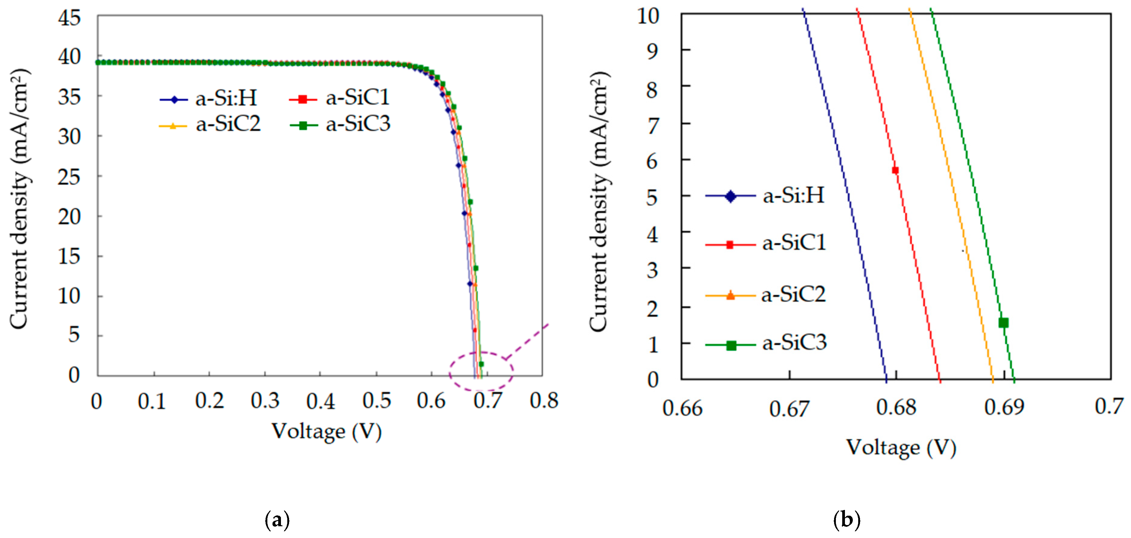
Figure 7a shows the J-V curves and performance of the SHJ solar cells with different a-SiC:H window layers. The curves near Voc are shown in Figure 7b. It is seen that open-circuit voltage is 679 mV when p-type a-Si:H is used. This value is relatively low as compared to that of state-of-the art HIT solar cells, which is beyond 720 mV, due to several possible reasons such as non-optimized intrinsic a-Si:H/c-Si interface or unsatisfied edge isolation. Therefore, the cell with a-Si:H window layer should only be used as a reference for comparison to observe the effect of a-SiC:H layer on performance of SHJ solar cells. The a-SiC:H window layers exhibit an increase in Voc by 4 to 11 mV. The short-circuit current density (Jsc) of the reference SHJ cells is 39.12 mA/cm2 and increases for the cells with a-SiC1 layer, or with a-SiC2 layer. The Jsc does not further increase for a-SiC3, which has the largest band gap among the a-SiC:H films. This is in accordance with the simulation result which shows the photogeneration rate for a-SiC3 is similar to the case of a-SiC2. The reduced collection efficiency of the holes due to the valence band offset might compensate the photocurrent gain brought by the larger band gap. This effect also leads to reduction in fill factor (FF). Besides, the conductivity of a-SiC:H films with higher carbon incorporation is lower. The FF decreases in the cases of those SHJ cells with high carbon-content a-SiC2 and a-SiC3. The series resistance of the SHJ cells can be extracted from the J-V curves by several methods [30,31,32]. Chang et al. [33] reported a simple solar cell parameter extraction method from a single J-V curve. By using this method, a plot of dV/dJ versus [(Jsc + J-V/Rsh)−1 kT/q] is illustrated, where J is the measured current density, V is the applied voltage, Rsh is the shunt resistance corresponding to the value of dV/dJ at the short-circuit condition, and kT/q is the thermal voltage. The series resistance can be obtained as the interception with the y-axis. The extracted series resistances are 1.46, 1.82, 2.17, and 2.2 Ωcm2 for the SHJ cells with a-Si:H, a-SiC1, a-SiC2, and a-SiC3, respectively. The increased series resistance also accounts for the decreased FF. Overall, the SHJ cell with a-SiC2 (band gap of 2 eV) has the highest conversion efficiency (η) of 22.16%.
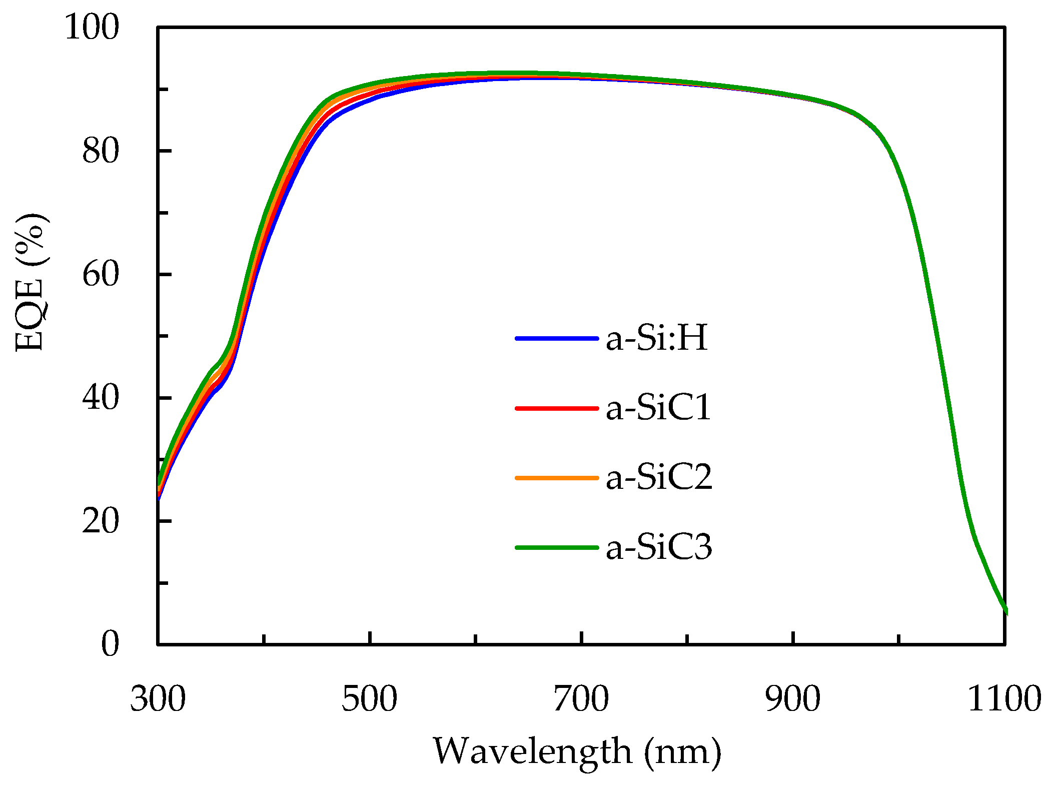
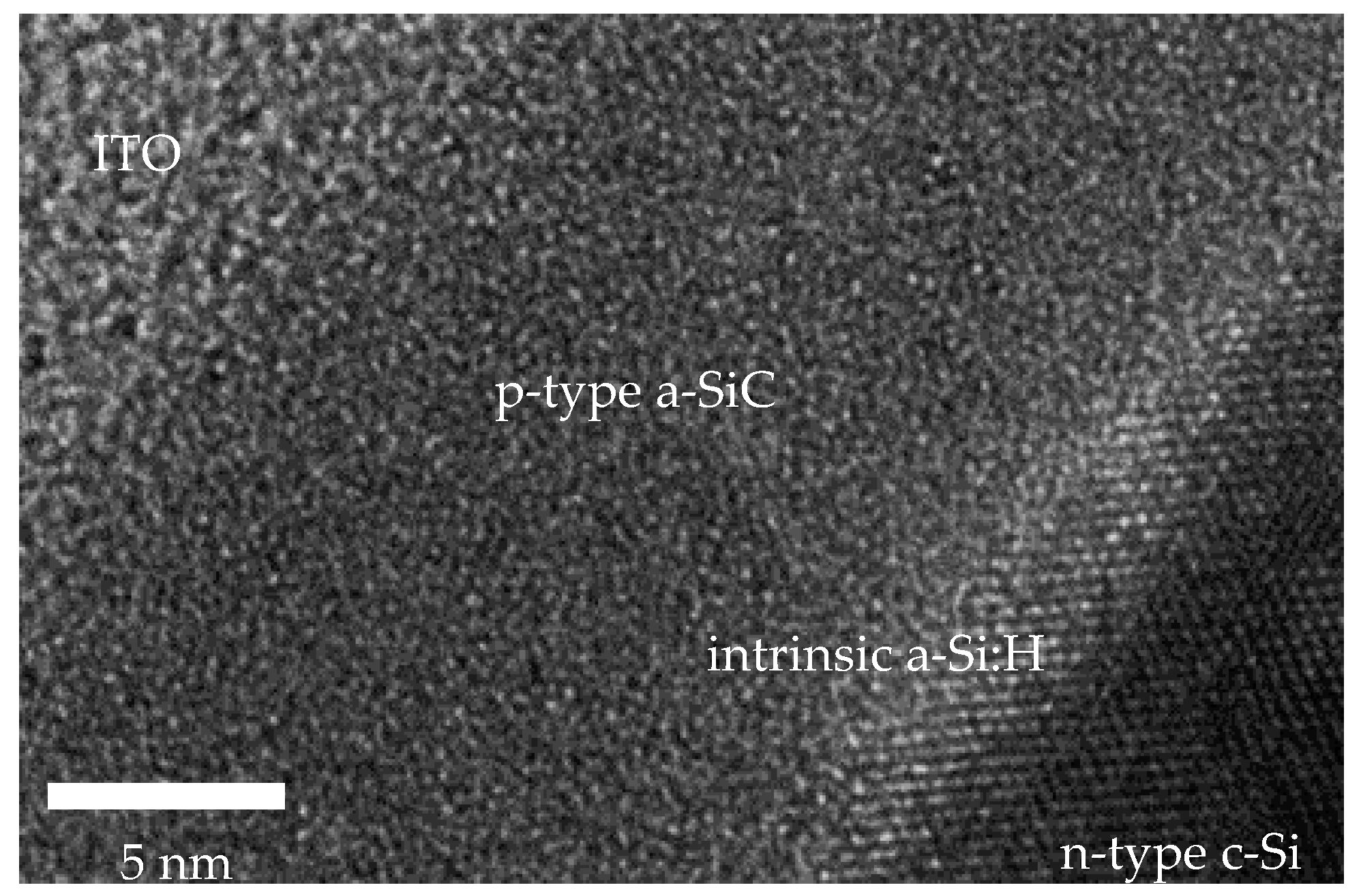
Figure 8 shows the EQE spectra of the SHJ solar cells with different p-type a-SiC:H window layer. The curves have nearly the same EQE values at long wavelengths, since the variation of the window layer would not significantly change the optical behavior at the rear side of the devices. For the short wavelengths, the a-Si:H window layer leads to the lowest spectral response. The a-SiC1 has the intermediate EQE values, and the a-SiC2 and a-SiC3 have the similar spectral response. This result accounts for the Jsc values. The cross-sectional TEM image of the fabricated SHJ solar cell with the p-type a-SiC2 window layer is shown in Figure 9. No ordered arrangement of the atoms can be observed in the p-type a-SiC2 layer, and thus the a-SiC2 layer is not crystallized.
4. Conclusions
P-type a-SiC:H films are deposited by 27.12 MHz PECVD with a gas mixture of SiH4, B2H6, H2 and CH4. The CH4 gas flow rate is varied to deposit films with different band gap. The experimental shows that a higher CH4 flow rate leads to increase in band gap, reduction in absorption coefficient, but the photoconductivity significantly reduces. Furthermore, the XPS result reveals that the boron content decrease when carbon incorporation increases. Therefore, there is a balance between the gain in band gap and the loss in conductivity. The TCAD simulation indicates that the photocurrent seems to saturate for the a-SiC:H with a band gap of 2 eV. The band structure reveals a large band gap can have more band bending that could enhance Voc, but band discontinuity presents at i/p interface. This might reduce carrier collecting, and eventually lower Jsc and FF of the devices. Finally, for SHJ solar cell fabrication, the cell with an intermediated band gap window layer exhibits the highest conversion efficiency of 22.14%, which is about 0.33% abs higher than those that use the a-Si:H window layer.
Author Contributions
Experiments, C.-H.H. and S.-Y.L.; formal analysis, C.-H.H., S.-Y.L., X.-Y.Z., W.-Z.Z. and H.-J.L.; writing—original draft preparation, C.-H.H.; writing—review and editing, S.-Y.L.; visualization, X.-Y.Z.; funding acquisition, X.-Y.Z. and M.J.Z.
Funding
This work is sponsored by the science and technology project of Xiamen (No. 3502Z20183054) and the Science and Technology Program of the Educational Office of Fujian Province (No. JT180432). This work is also supported by the National Natural Science Foundation of China (grant No. 61704142).
Conflicts of Interest
The authors declare no conflict of interest.
References
- Yoshikawa, K.; Kawasaki, H.; Yoshida, W.; Irie, T.; Konishi, K.; Nakano, K.; Uto, T.; Adachi, D.; Kanematsu, M.; Uzu, H.; et al. Silicon heterojunction solar cell with interdigitated back contacts for a photoconversion efficiency over 26%. Nat. Energy 2017, 2, 17032. [Google Scholar] [CrossRef]
- Taguchi, M.; Yano, A.; Tohoda, S.; Matsuyama, K.; Nakamura, Y.; Nishiwaki, T.; Fujita, K.; Maruyama, E. 24.7% Record efficiency HIT solar cell on thin silicon wafer. IEEE J. Photovolt. 2014, 4, 96–99. [Google Scholar] [CrossRef]
- DeWolf, S.; Descoeudres, A.; Holman, Z.C.; Ballif, C. High-efficiency silicon heterojunction solar cells: A review. Green 2012, 2, 7–24. [Google Scholar]
- Mueller, T.; Wong, J.; Aberle, A.G. Heterojunction silicon wafer solar cells using amorphous silicon suboxides for interface passivation. Energy Procedia 2012, 15, 97–106. [Google Scholar] [CrossRef]
- Descoeudres, A.; Allebé, C.; Badel, N.; Barraud, L.; Champliaud, J.; Debrot, F.; Faes, A.; Lachowicz, A.; Levrat, J.; Nicolay, S.; et al. Silicon Heterojunction Solar Cells: Towards Low-cost High-Efficiency Industrial Devices and Application to Low-concentration PV. Energy Procedia 2015, 77, 508–514. [Google Scholar] [CrossRef] [Green Version]
- Stanislau, Y.; Herasimenka, W.J.D.; Bowden, S.G. > 750 mV open circuit voltage measured on 50 μm thick silicon heterojunction solar cell. Appl. Phys. Lett. 2013, 103, 053511. [Google Scholar]
- Holman, Z.C.; Descoeudres, A.; Barraud, L.; Fernandez, F.Z.; Seif, J.P.; Wolf, S.D.; Ballif, C. Current Losses at the Front of Silicon Heterojunction Solar Cells. IEEE J. Photovolt. 2012, 2, 7–15. [Google Scholar] [CrossRef]
- Ding, K.; Aeberhard, U.; Finger, F.; Rau, U. Silicon heterojunction solar cell with amorphous silicon oxide buffer and microcrystalline silicon oxide contact layers. Phys. Status Solidi Rapid Res. Lett. 2012, 6, 193–195. [Google Scholar] [CrossRef]
- Battaglia, C.; DeNicolás, S.M.; DeWolf, S.; Yin, X.; Zheng, M.; Ballif, C.; Javey, A. Silicon heterojunction solar cell with passivated hole selective MoOx contact. Appl. Phys. Lett. 2014, 104, 113902. [Google Scholar] [CrossRef]
- Peter Seif, J.; Descoeudres, A.; Filipič, M.; Smole, F.; Topič, M.; Charles Holman, Z.; DeWolf, S.; Ballif, C. Amorphous silicon oxide window layers for high-efficiency silicon heterojunction solar cells. J. Appl. Phys. 2014, 115, 024502. [Google Scholar] [CrossRef] [Green Version]
- Sritharathikhun, J.; Jiang, F.; Miyajima, S.; Yamada, A.; Konagai, M. Optimization of p-type hydrogenated microcrystalline silicon oxide window layer for high-efficiency crystalline silicon heterojunction solar cells. Jpn. J. Appl. Phys. 2009, 48, 1016031–1016035. [Google Scholar] [CrossRef]
- Lu, M.; Bowden, S.; Das, U.; Birkmire, R. Interdigitated back contact silicon heterojunction solar cell and the effect of front surface passivation. Appl. Phys. Lett. 2007, 91, 063507. [Google Scholar] [CrossRef]
- Green, M.A.; Emery, K.; Hishikawa, Y.; Warta, W.; Dunlop, E.D. Solar cell efficiency tables (Version 45). Prog. Photovolt. 2015, 23, 1–9. [Google Scholar] [CrossRef]
- Yang, J.; Banerjee, A.; Guha, S. Amorphous silicon based photovoltaics–From earth to the “final frontier”. Sol. Energy Mater. Sol. Cells 2003, 78, 597–612. [Google Scholar] [CrossRef]
- Andoh, N.; Nagayoshi, H.; Kanbashi, T.; Kamisako, K. Characterization of high-quality a-SiC: H films prepared by hydrogen-radical CVD method. Sol. Energy Mater. Sol. Cells 1997, 49, 89–94. [Google Scholar] [CrossRef]
- Wang, Y.H.; Lin, J.; Huan, C.H. Multiphase structure of hydrogenated amorphous silicon carbide thin films. Mater. Sci. Eng. B 2002, 95, 43. [Google Scholar] [CrossRef]
- Bullot, J.; Schmidt, M.P. Physics of Amorphous Silicon–Carbon Alloys. Phys. Status Solidi B 1987, 143, 345. [Google Scholar] [CrossRef]
- Vasin, A.V.; Kolesnik, S.P.; Konchits, A.A.; Rusavsky, A.V.; Lysenko, V.S.; Nazarov, A.N.; Ishikawa, Y.; Koshka, Y. Structure, paramagnetic defects and light-emission of carbon-rich a-SiC:H films. J. Appl. Phys. 2008, 103, 123710. [Google Scholar] [CrossRef]
- Robertson, J. Defects in Diamond-Like Carbon. J. Phys. Status Solidi A 2001, 186, 177. [Google Scholar] [CrossRef]
- Yao, Y.; Xiao, S.; Zhang, X.; Gu, X. Simulation optimizing of n type HIT solar cells with AFORS-HET Mod. Phys. Lett. B 2017, 31, 1740025. [Google Scholar]
- Lisheng, W.; Fengxiang, C.; Yu, A. Simulation of high efficiency heterojunction solar cells with AFORS-HET. J. Phys. Conf. Ser. 2011, 276, 012177. [Google Scholar] [CrossRef]
- Fortes, M.; Belfar, A.; Garcia-Loureiro, A.J. Two-dimensional simulation study of textured p-i-n a-Si:H solar cells with p-a-SiC:H and p-nc-Si:H window layers. Optik 2016, 127, 9464–9473. [Google Scholar] [CrossRef]
- Cannella, G.; Principato, F.; Foti, M.; Di Marco, S.; Grasso, A.; Lombardo, S. Carrier transport mechanism in the SnO2: F/p-type a-Si:H heterojunction. J. Appl. Phys. 2011, 110, 024502. [Google Scholar] [CrossRef]
- Liu, Y.; Sun, Y.; Liu, W.; Yao, J.H. Novel high-efficiency crystalline-silicon-based compound heterojunction solar cells: HCT (heterojunction with compound thin-layer). Phys. Chem. Chem. Phys. 2014, 16, 15400. [Google Scholar] [CrossRef]
- Baek, S.; Lee, J.; Lee, Y.-J.; Iftiquar, S.M.; Kim, Y.; Park, J.; Yi, J. Interface modification effect between p-type a-SiC:H and ZnO: Al in p-i-n amorphous silicon solar cells. Nanoscale Res. Lett. 2012, 7, 81. [Google Scholar] [CrossRef]
- Dao, V.A.; Lee, Y.; Kim, S.; Cho, J.; Ahn, S.; Kim, Y.; Lakshminarayan, N.; Yi, J. Effect of Valence Band Offset and Surface Passivation Quality in the Silicon Heterojunction Solar Cells. J. Electrochem. Soc. 2011, 158, H1129. [Google Scholar] [CrossRef]
- Shen, L.; Meng, F.; Liu, Z. Roles of the Fermi level of doped a-Si: H and band offsets at a-Si: H/c-Si interfaces in n-type HIT solar cells. Sol. Energy 2013, 97, 168–175. [Google Scholar] [CrossRef]
- Wang, F.; Du, R.; Ren, Q.; Wei, C.; Zhao, Y.; Zhang, X. Band alignment and enhancement of the interface properties for heterojunction solar cells by employing amorphous–nanocrystalline hierarchical emitter layers. J. Mater. Chem. C 2017, 5, 1751–1757. [Google Scholar] [CrossRef]
- Pham, D.P.; Kim, S.; Park, J.; Cho, J.; Kim, H.; Le, A.H.T.; Yi, J. Role of a-Si:H buffer layer at the p/i interface and band gap profiling of the absorption layer on enhancing cell parameters in hydrogenated amorphous silicon germanium solar cells. Optik 2017, 136, 507–512. [Google Scholar] [CrossRef]
- Yu, F.; Huang, G.; Lin, W.; Xu, C. An analysis for S-shaped I-V characteristics of organic solar cells using lumped-parameter equivalent circuit model. Sol. Energy 2019, 177, 229–240. [Google Scholar] [CrossRef]
- Huang, G.; Yu, F.; Xu, C. An Analytical Solution to Lumped Parameter Equivalent Circuit Model of Organic Solar Cells. Crystals 2018, 8, 224. [Google Scholar] [CrossRef]
- Yu, F.; Huang, G.; Lin, W.; Xu, C. Lumped-Parameter Equivalent Circuit Model for S-Shaped Current–Voltage Characteristics of Organic Solar Cells. IEEE Trans. Electron Devices 2019, 66, 670–677. [Google Scholar] [CrossRef]
- Zhang, C.F.; Zhang, J.C.; Hao, Y.; Lin, Z.H.; Zhu, C.X. A simple and efficient solar cell parameter extraction method from a single current-voltage curve. J. Appl. Phys. 2011, 110, 064504. [Google Scholar] [CrossRef] [Green Version]
Figure 1.
Scheme of a silicon heterojunction (SHJ) solar cell. The arrows indicate the incident light.
Figure 1.
Scheme of a silicon heterojunction (SHJ) solar cell. The arrows indicate the incident light.

Figure 2.
Absorption coefficient of a-SiC:H films with different H2/CH4 gas flow ratio as a function of wavelength.
Figure 2.
Absorption coefficient of a-SiC:H films with different H2/CH4 gas flow ratio as a function of wavelength.

Figure 3.
Band gap, photoconductivity and dark conductivity of the p-type a-SiC:H films deposited with different CH4 gas flow rate.
Figure 3.
Band gap, photoconductivity and dark conductivity of the p-type a-SiC:H films deposited with different CH4 gas flow rate.

Figure 4.
Atomic ratio of Si, C and B of the a-SiC:H films deposited with different CH4 gas flow rate.
Figure 4.
Atomic ratio of Si, C and B of the a-SiC:H films deposited with different CH4 gas flow rate.

Figure 5.
Depth profile of photogeneration rate (G) of SHJ solar cells. The inset is the close view of the red-marked region.
Figure 5.
Depth profile of photogeneration rate (G) of SHJ solar cells. The inset is the close view of the red-marked region.

Figure 6.
Simulated band structure of SHJ solar cells with different p-type a-SiC:H window layer.

Figure 7.
(a) Current density-voltage (J-V) curves and performance of the fabricated SHJ solar cells with different p-type a-SiC:H window layer. (b) Close-up view of the J-V curves near open-circuit voltage.
Figure 7.
(a) Current density-voltage (J-V) curves and performance of the fabricated SHJ solar cells with different p-type a-SiC:H window layer. (b) Close-up view of the J-V curves near open-circuit voltage.

Figure 8.
External quantum efficiency (EQE) spectra for the SHJ solar cells with different p-type a-SiC:H window layer.
Figure 8.
External quantum efficiency (EQE) spectra for the SHJ solar cells with different p-type a-SiC:H window layer.

Figure 9.
Cross-sectional transmission electron microscope (TEM) image of the silicon heterojunction solar cell with the p-type a-SiC2 layer.
Figure 9.
Cross-sectional transmission electron microscope (TEM) image of the silicon heterojunction solar cell with the p-type a-SiC2 layer.


Table 1.
Deposition conditions for plasma enhanced chemical vapor deposition (PECVD) hydrogenated amorphous silicon carbide (a-SiC:H) thin films.
Table 1.
Deposition conditions for plasma enhanced chemical vapor deposition (PECVD) hydrogenated amorphous silicon carbide (a-SiC:H) thin films.
| Parameter | Value |
|---|---|
| Power (W) | 10 |
| Pressure (Pa) | 80 |
| Substrate Temperature (°C) | 250 |
| Thickness (μm) | 0.5 |
| Process time (min) | 40 |
| SiH4 flow rate (sccm) | 20 |
| B2H6 flow rate (sccm) | 10 |
| CH4 flow rate (sccm) | 0~50 |
| H2 flow rate (sccm) | 90~40 |
Table 2.
Deposition conditions for hydrogenated amorphous silicon (a-Si:H), a-SiC1, a-SiC2 and a-SiC3 thin films.
Table 2.
Deposition conditions for hydrogenated amorphous silicon (a-Si:H), a-SiC1, a-SiC2 and a-SiC3 thin films.
| Parameter | a-Si:H | a-SiC1 | a-SiC2 | a-SiC3 |
|---|---|---|---|---|
| Power (W) | 10 | 10 | 10 | 10 |
| Pressure (Pa) | 80 | 80 | 80 | 80 |
| Substrate Temperature (°C) | 200 | 200 | 200 | 200 |
| Thickness (μm) | 0.5 | 0.5 | 0.5 | 0.5 |
| Process time (min) | 40 | 40 | 40 | 40 |
| SiH4 flow rate (sccm) | 20 | 20 | 20 | 20 |
| B2H6 flow rate (sccm) | 10 | 10 | 10 | 10 |
| CH4 flow rate (sccm) | 0 | 10 | 30 | 50 |
| H2 flow rate (sccm) | 90 | 80 | 60 | 40 |
© 2019 by the authors. Licensee MDPI, Basel, Switzerland. This article is an open access article distributed under the terms and conditions of the Creative Commons Attribution (CC BY) license (http://creativecommons.org/licenses/by/4.0/).
Share and Cite
MDPI and ACS Style
Hsu, C.-H.; Zhang, X.-Y.; Zhao, M.J.; Lin, H.-J.; Zhu, W.-Z.; Lien, S.-Y. Silicon Heterojunction Solar Cells with p-Type Silicon Carbon Window Layer. Crystals 2019, 9, 402. https://0-doi-org.brum.beds.ac.uk/10.3390/cryst9080402
AMA Style
Hsu C-H, Zhang X-Y, Zhao MJ, Lin H-J, Zhu W-Z, Lien S-Y. Silicon Heterojunction Solar Cells with p-Type Silicon Carbon Window Layer. Crystals. 2019; 9(8):402. https://0-doi-org.brum.beds.ac.uk/10.3390/cryst9080402
Chicago/Turabian StyleHsu, Chia-Hsun, Xiao-Ying Zhang, Ming Jie Zhao, Hai-Jun Lin, Wen-Zhang Zhu, and Shui-Yang Lien. 2019. "Silicon Heterojunction Solar Cells with p-Type Silicon Carbon Window Layer" Crystals 9, no. 8: 402. https://0-doi-org.brum.beds.ac.uk/10.3390/cryst9080402
Note that from the first issue of 2016, this journal uses article numbers instead of page numbers. See further details here.