
19% Efficient P3CT-Na Based MAPbI3 Solar Cells with a Simple Double-Filtering Process

 , ,
, ,
Abstract
:
1. Introduction
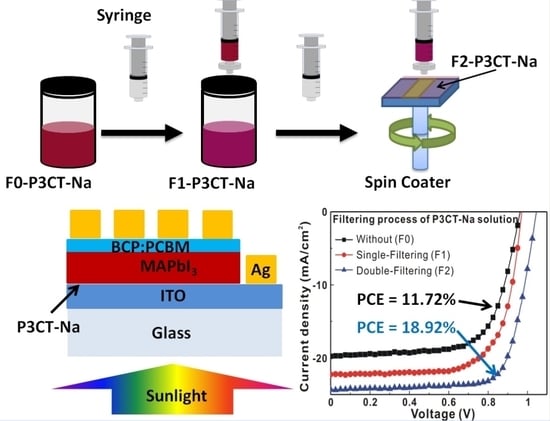
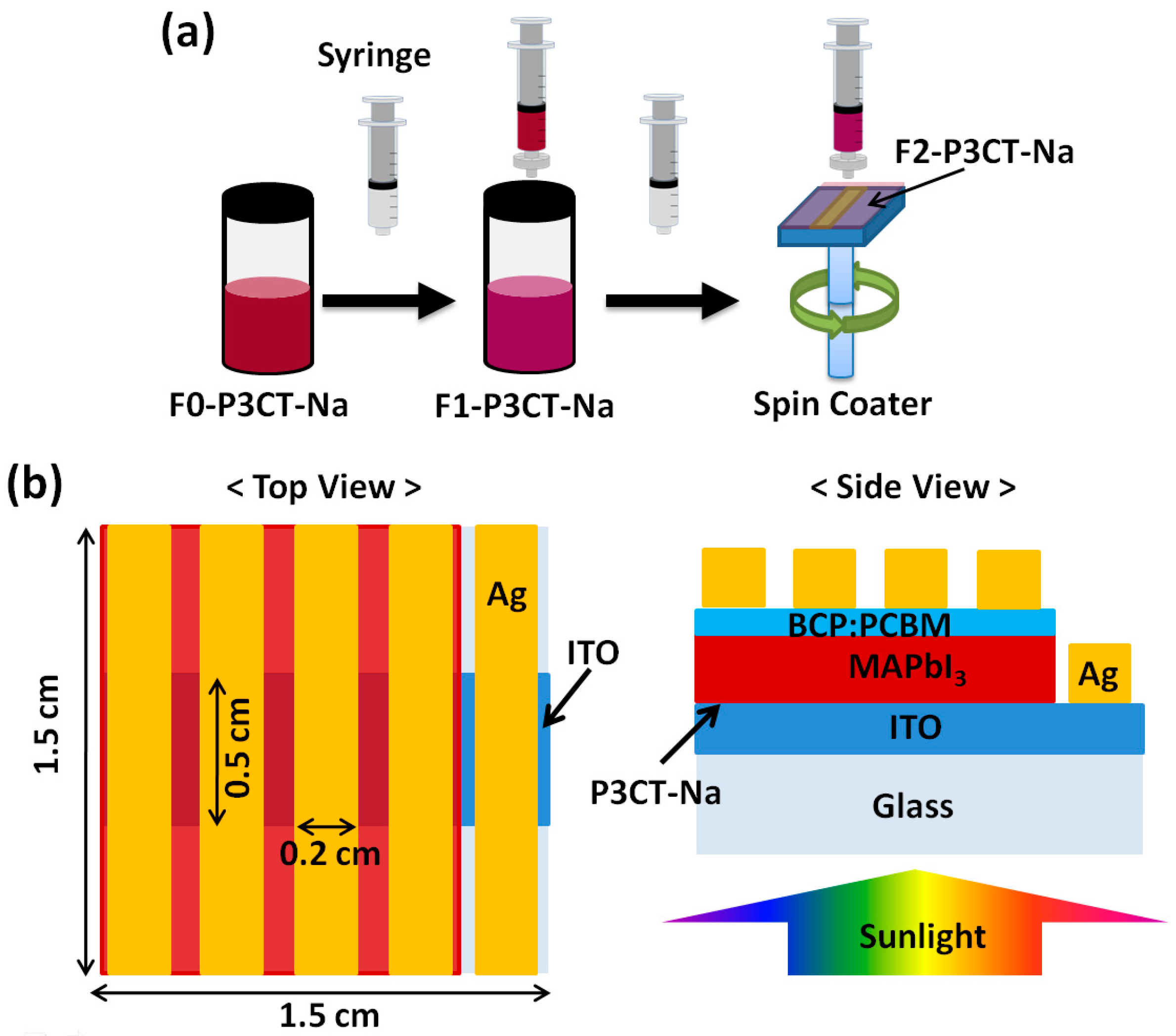
2. Experiments
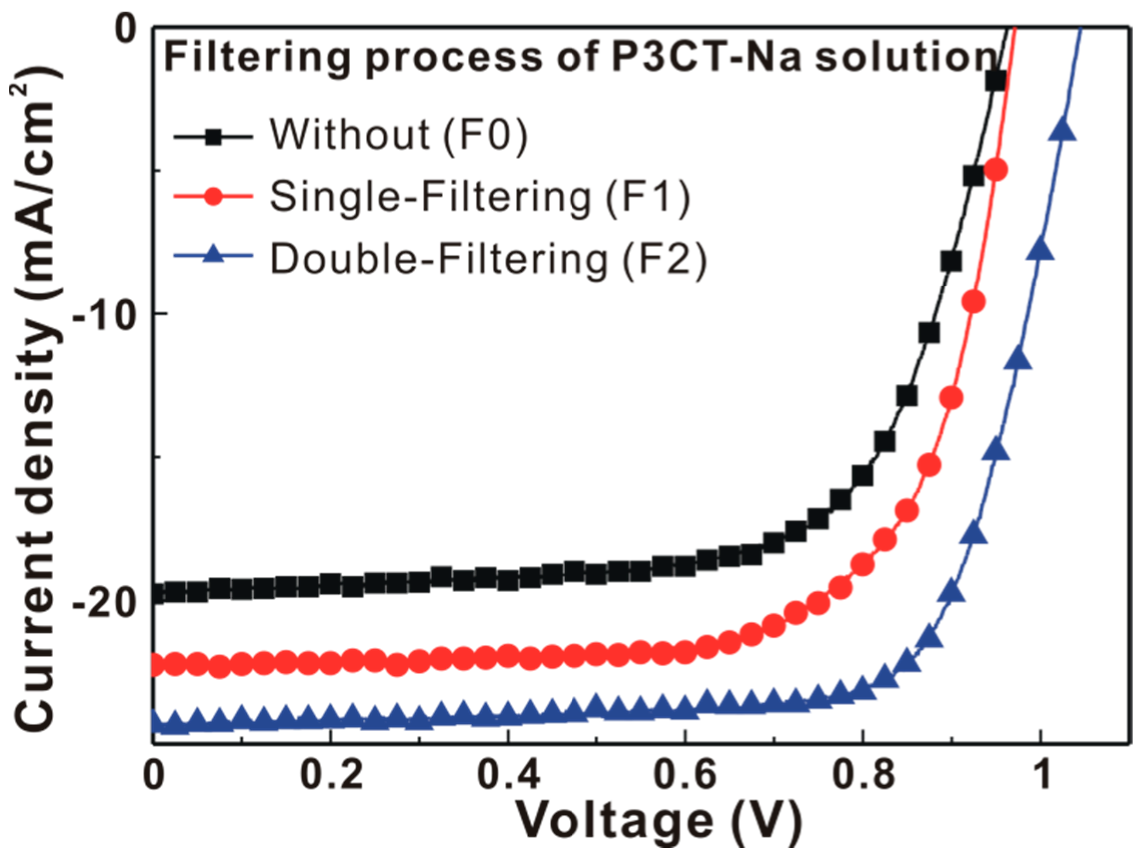
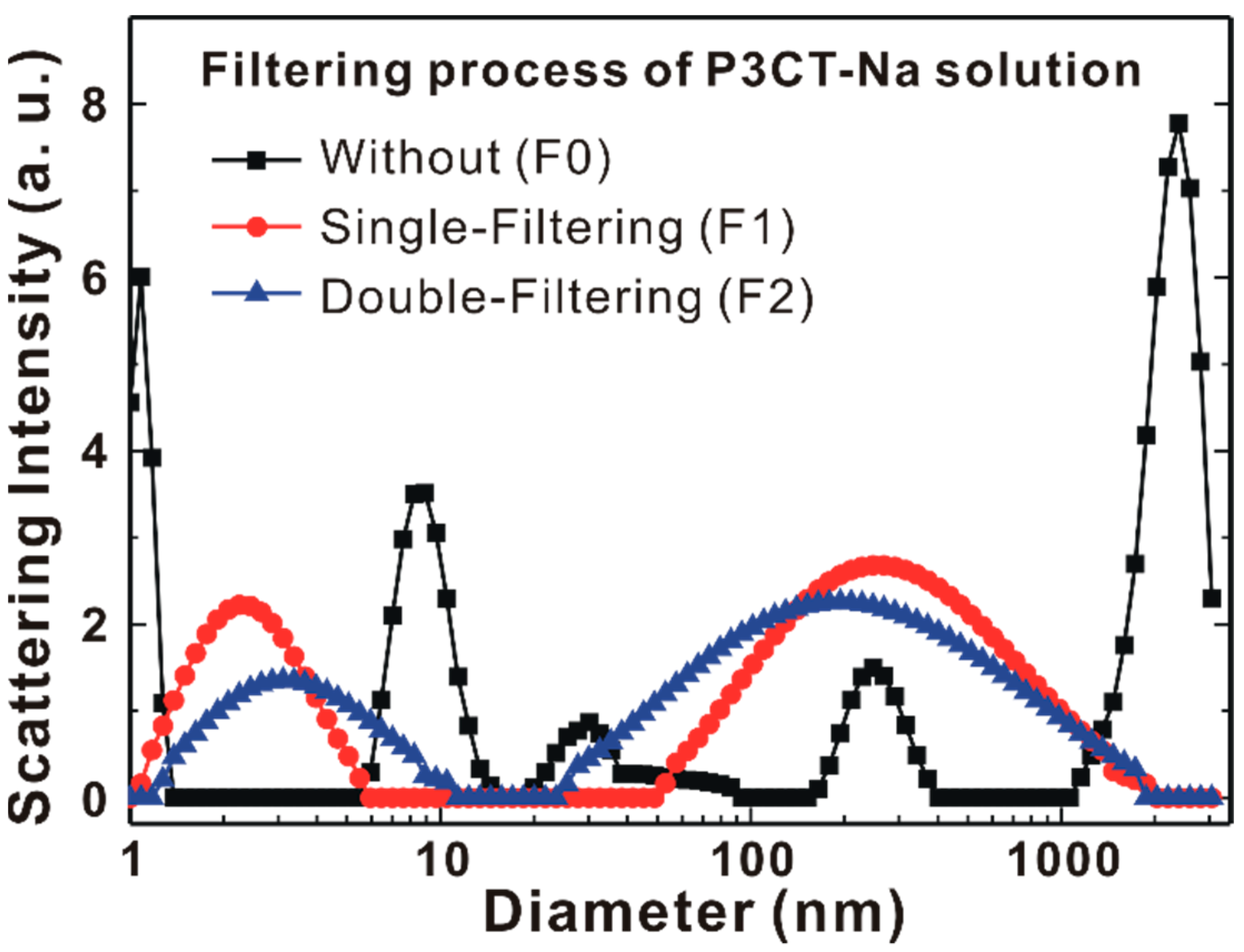
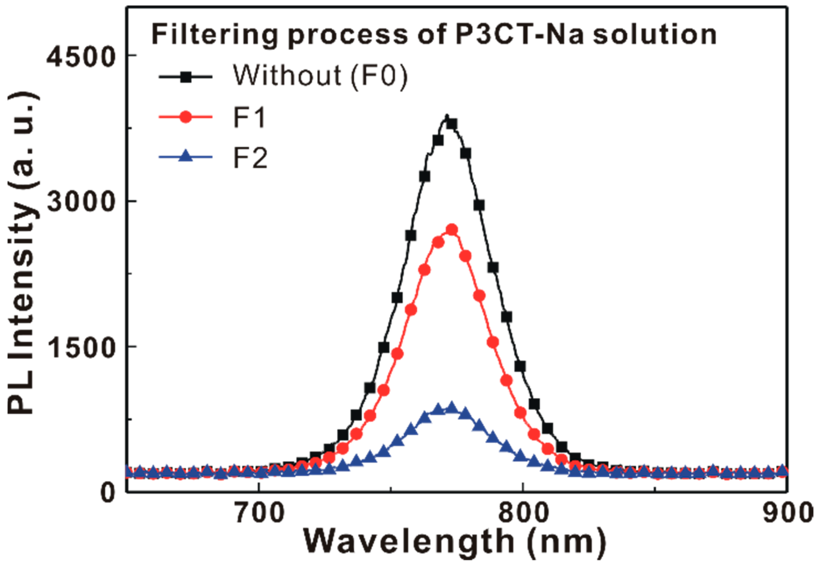
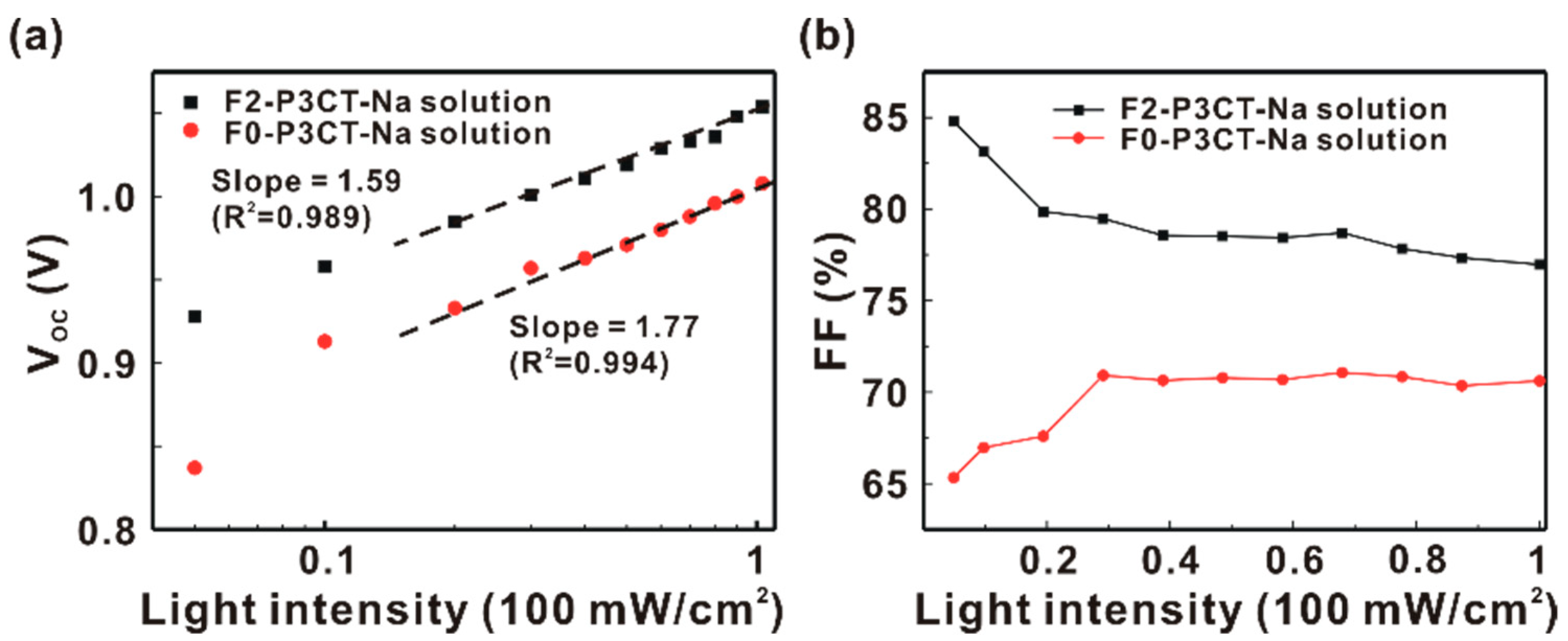
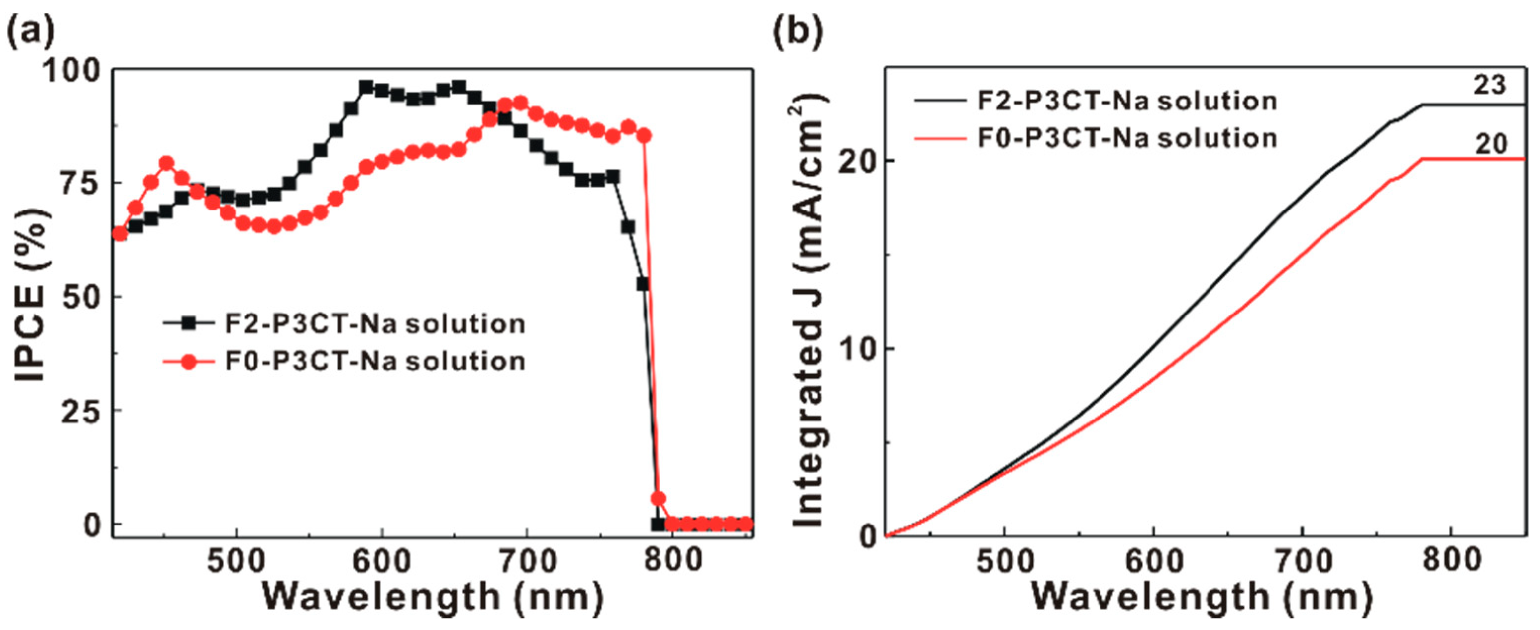
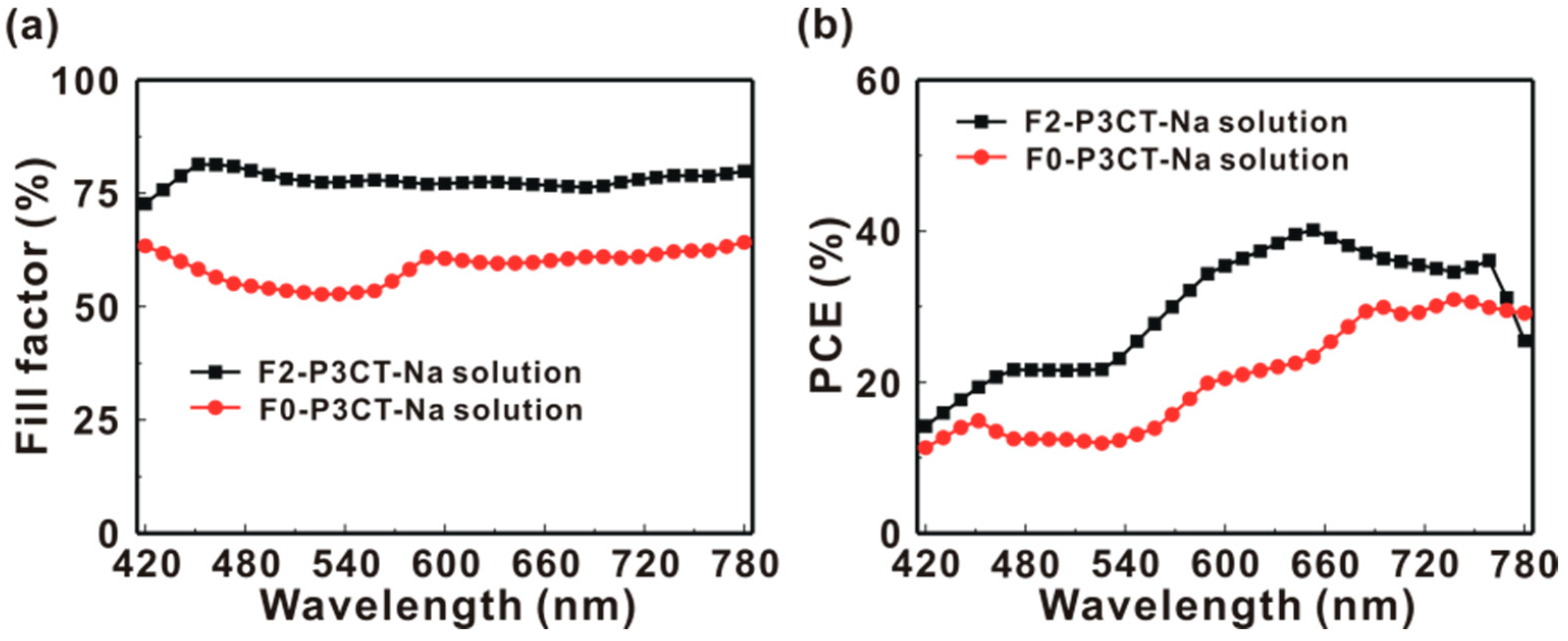
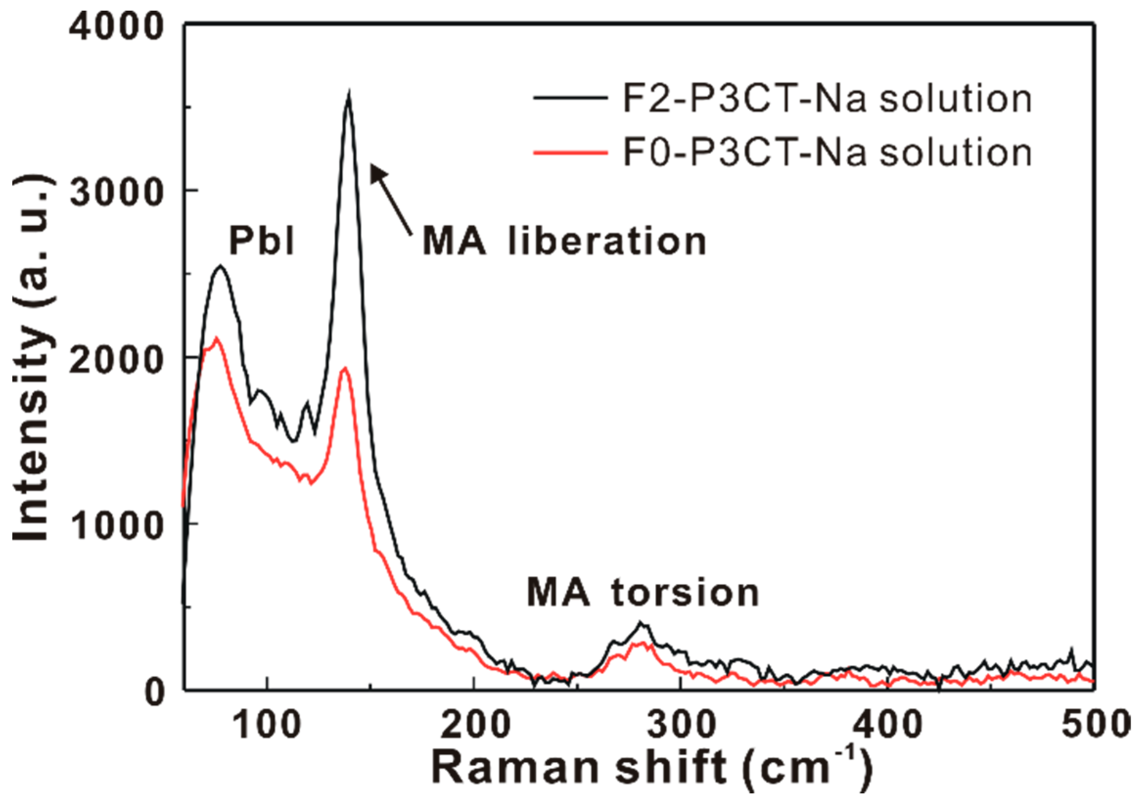
3. Results and Discussion
4. Conclusions
Author Contributions
Funding
Institutional Review Board Statement
Informed Consent Statement
Data Availability Statement
Conflicts of Interest
References
- NREL, Research Cell Efficiency Record. 2020. Available online: https://www.nrel.gov/pv/assets/pdfs/best-research-cell-efficiencies.20200104.pdf (accessed on 31 October 2020).
- Zheng, X.; Hou, Y.; Bao, C.; Yin, J.; Yuan, F.; Huang, Z.; Song, K.; Liu, J.; Troughton, J.; Gasparini, N.; et al. Managing grains and interfaces via ligand anchoring enables 22.3%-efficiency inverted perovskite solar cells. Nat. Energy 2020, 5, 131–140. [Google Scholar] [CrossRef]
- Lin, C.-P.; Chen, H.; Nakaruk, A.; Koshy, P.; Sorrell, C.C. Effect of annealing temperature on the photocatalytic activity of TiO2 thin films. Energy Procedia 2013, 34, 627–636. [Google Scholar] [CrossRef] [Green Version]
- Lin, K.-F.; Chang, S.H.; Wang, K.-H.; Cheng, H.-M.; Chiu, K.Y.; Lee, K.-M.; Chen, S.-H.; Wu, C.-G. Unraveling the high performance of tri-iodide perovskite absorber based photovoltaics with a non-polar solvent washing treatment. Sol. Energy Mater. Sol. Cells 2015, 141, 309–314. [Google Scholar] [CrossRef]
- Chang, S.H.; Lin, K.-F.; Chiu, K.Y.; Tsai, C.-L.; Cheng, H.-M.; Yeh, S.-C.; Wu, W.-T.; Chen, W.-N.; Chen, C.-T.; Chen, S.-H.; et al. Improving the efficiency of CH3NH3PbI3 based photovoltaics by tuning the work function of the PEDOT:PSS hole transport layer. Sol. Energy 2015, 122, 892–899. [Google Scholar] [CrossRef]
- Chen, C.-C.; Chang, S.-H.; Chen, L.-C.; Kao, F.-S.; Cheng, H.-M.; Yeh, S.-C.; Chen, C.-T.; Wu, W.-T.; Tseng, Z.-L.; Chuang, C.L.; et al. Improving the efficiency of inverted mixed-organic-cation perovskite absorber based photovoltaics by tailing the surface roughness of PEDOT:PSS thin film. Sol. Energy 2016, 134, 445–451. [Google Scholar] [CrossRef]
- Chang, S.H.; Chen, W.-N.; Chen, C.-C.; Yeh, S.-C.; Cheng, H.-M.; Tseng, Z.-L.; Chen, L.-C.; Chiu, K.Y.; Wu, W.-T.; Chen, C.-T.; et al. Manipulating the molecular structure of PEDOT chains through controlling the viscosity of PEDOT:PSS solutions improve the photovoltaic performance of CH3NH3PbI3 solar cells. Sol. Energy Mater. Sol. Cells 2017, 161, 7–13. [Google Scholar] [CrossRef]
- Huang, D.; Goh, T.; Kong, J.; Zheng, Y.; Zhao, S.; Xu, Z.; Taylor, A.D. Perovskite solar cells with a DMSO-treated PEDOT:PSS hole transport layer exhibit higher photovoltaic performance and enhanced durability. Nanoscale 2017, 9, 4236–4243. [Google Scholar] [CrossRef] [PubMed]
- Chiang, S.-E.; Wu, J.-R.; Cheng, H.-M.; Hsu, C.-L.; Shen, J.-L.; Yuan, C.-T.; Chang, S.H. Origins of the s-shape characteristic in J-V curve of inverted-type perovskite solar cells. Nanotechnology 2020, 31, 115403. [Google Scholar] [CrossRef]
- Li, C.-Y.; Liao, Y.-S.; Thakur, D.; Chandel, A.; Chiang, S.-E.; Wu, J.-R.; Lee, P.-H.; Tsai, C.-L.; Yang, C.-C.; Zhong, Y.-L.; et al. Anti-solvent mixture-mediated reduction of photocurrent hysteresis in high-impurity perovskite precursor based MAPbI3 solar cells. Sol. Energy 2021, 214, 86–92. [Google Scholar] [CrossRef]
- Yu, Z.-K.; Fu, W.-F.; Liu, W.-Q.; Zhang, Z.-Q.; Liu, Y.-H.; Yan, J.-L.; Yang, W.-T.; Li, H.-Y.; Chen, Z.-Z. Solution-processed CuOx as an efficient hole-extraction layer for inverted planar heterojunction perovskite solar cells. Chin. Chem. Lett. 2017, 28, 13–18. [Google Scholar] [CrossRef] [Green Version]
- Islam, M.B.; Yanagida, M.; Shirai, Y.; Nabetani, Y.; Miyano, K. NiOx hole transport layer for perovskite solar cells with improved stability and reproducibility. ACS Omega 2017, 2, 2291–2299. [Google Scholar] [CrossRef] [Green Version]
- Chen, W.; Pang, G.; Zhou, Y.; Sun, Y.; Liu, F.-Z.; Chen, R.; Chen, S.; Djurisic, A.B.; He, Z. Stabilizing n-type hetero-junctions for NiOx based inverted planar perovskite solar cells with an efficiency of 21.6%. J. Mater. Chem. A 2020, 8, 1865–1874. [Google Scholar] [CrossRef]
- Lin, Y.-R.; Liao, Y.-S.; Hsaio, H.-T.; Chen, C.-P. Two-step annealing of NiOx enhances the NiOx-perovskite interface for high-performance ambient-stable p-i-n perovskite solar cells. Appl. Surf. Sci. 2020, 504, 144478. [Google Scholar] [CrossRef]
- Li, X.; Liu, X.; Wang, X.; Zhao, L.; Jiu, T.; Fang, J. Polyelectrolyte based hole-transporting materials for high performance solution processed planar perovskite solar cells. J. Mater. Chem. A 2015, 3, 15024–15029. [Google Scholar] [CrossRef]
- Li, X.; Wang, Y.-C.; Zhu, L.; Zhang, W.; Wang, H.-Q.; Fang, J. Improving efficiency and reproducibility of perovskite solar cells through aggregation control in polyelectrolytes hole transport layer. ACS Appl. Mater. Interfaces 2017, 9, 31357–31361. [Google Scholar] [CrossRef]
- Li, J.; Zhao, M.; Zhao, C.; Jian, H.; Wang, N.; Yao, L.; Huang, C.; Zhao, Y.; Jiu, T. Graphdiyne-doped P3CT-K as an efficient hole-transport layer for MAPbI3 perovskite solar cells. ACS Appl. Mater. Interfaces 2019, 11, 2626–2631. [Google Scholar] [CrossRef]
- Li, S.; He, B.; Xu, J.; Lu, H.; Jiang, J.; Zhu, J.; Kan, Z.; Zhu, L.; Wu, F. Highly efficient inverted perovskite solar cells incorporating P3CT-Rb as a hole transport layer to achieve a large open circuit voltage of 1.144 V. Nanoscale 2020, 12, 3686–3691. [Google Scholar] [CrossRef]
- Lanzi, M.; Salatelli, E.; Giorgini, L.; Mucci, A.; Pierini, F.; Di-Nicola, F.P. Water-soluble polythiophenes as efficient charge-transport layers for the improvement of photovoltaic performance in bulk heterojunction polymeric solar cells. Eur. Polym. J. 2017, 97, 378–388. [Google Scholar] [CrossRef]
- Vohra, V.; Shimizu, S.; Takeoka, Y. Water-processed organic solar cells with open-circuit voltages exceeding 1.3 V. Coatings 2020, 10, 421. [Google Scholar] [CrossRef]
- Jeon, N.J.; Noh, J.H.; Kim, Y.C.; Yang, W.S.; Ryu, S.; Seok, S.I. Solvent engineering for high-performance inorganic-organic hybrid perovskite solar cells. Nat. Mater. 2014, 13, 897–903. [Google Scholar] [CrossRef] [PubMed]
- Xiao, M.; Huang, F.; Huang, W.; Dihissi, Y.; Zhu, Y.; Etheridge, J.; Gray-Weale, A.; Bach, U.; Cheng, Y.-B.; Spiccia, L. A fast deposition-crystallization procedure for highly efficient lead iodide perovskite thin-film solar cells. Angew. Chem. Int. Ed. 2014, 53, 9898–9903. [Google Scholar] [CrossRef] [PubMed]
- Chang, S.H.; Wong, S.-D.; Huang, H.-Y.; Yuan, C.-T.; Wu, J.-R.; Chiang, S.-E.; Tseng, Z.-L.; Chen, S.-H. Effects of the washing-enhanced nucleation process on the material properties and performance of perovskite solar cells. J. Alloys Compd. 2019, 808, 151732. [Google Scholar] [CrossRef]
- Chang, S.H.; Tseng, P.-C.; Chiang, S.-E.; Wu, J.-R.; Chen, Y.-T.; Chen, C.-J.; Yuan, C.-T.; Chen, S.-H. Structural, optical and excitonic properties of MAxCs1-xPb(IxBr1-x)3 alloy thin films and their application in solar cells. Sol. Energy Mater. Sol. Cells 2020, 210, 110478. [Google Scholar] [CrossRef]
- So, S.K.; Choi, W.K.; Cheng, C.H.; Leung, L.M.; Kwong, C.F. Surface preparation and characterization of indium tin oxide substrates for organic electroluminescent devices. Appl. Phys. A 1999, 68, 447–450. [Google Scholar] [CrossRef]
- Quarti, C.; Mosconi, E.; Ball, J.M.; D’Innocenzo, V.; Tao, C.; Pathak, S.; Snaith, H.J.; Petrozza, A.; De Angelis, F. Structural and optical properties of methylammonium lead iodide across the tetragonal to cubic phase transition: Implications to perovskite solar cells. Energy Environ. Sci. 2016, 9, 155–163. [Google Scholar] [CrossRef]
- Chang, S.H.; Lin, K.-F.; Chiang, C.-H.; Chen, S.-H.; Wu, C.-G. Plasmonic structure enhanced exciton generation at the interface between the perovskite absorber and copper nanoparticles. Sci. World J. 2014, 2014, 128414. [Google Scholar] [CrossRef]
- Koster, L.J.A.; Mihailetchi, V.D.; Ramaker, R.; Blom, P.W.M. Light intensity dependence of open-circuit voltage of polymer:fullerene solar cells. Appl. Phys. Lett. 2005, 86, 123509. [Google Scholar] [CrossRef] [Green Version]
- Caprioglio, P.; Stolterfoht, M.; Wolff, C.M.; Unold, T.; Rech, B.; Albrecht, S.; Neher, D. On the relation between the open-circuit voltage and quasi-Fermi level splitting in efficient perovskite solar cells. Adv. Energy Mater. 2019, 9, 1901631. [Google Scholar] [CrossRef] [Green Version]
- Liu, M.; Endo, M.; Shimazaki, A.; Wakamiya, A.; Tachibana, Y. Light intensity dependence of performance of lead halide perovskite solar cells. J. Photopolym. Sci. Technol. 2017, 5, 577–582. [Google Scholar] [CrossRef] [Green Version]
- Du, T.; Xu, W.; Xu, S.; Ratnasingham, S.R.; Lin, C.-T.; Kim, J.; Briscoe, J.; McLachlan, M.A.; Durrant, J.R. Light-intensity and thickness dependent efficiency of planar perovskite solar cells: Charge recombination versus extraction. J. Mater. Chem. C 2020, 8, 12648–12655. [Google Scholar] [CrossRef]
- Frost, J.M.; Bulter, K.T.; Brivio, F.; Hendon, C.H.; Van Schilfgaarde, M.; Walsh, A. Atomistic origins of high-performance in hybrid halide perovskite solar cells. Nano Lett. 2014, 14, 2584–2590. [Google Scholar] [CrossRef] [PubMed] [Green Version]
- Leguy, A.M.A.; Azarhoosh, P.; Alonso, M.I.; Campoy-Quiles, M.; Weber, O.J.; Yao, J.; Bryant, D.; Weller, M.T.; Nelson, J.; Walsh, A.; et al. Experimental and theoretical optical properties of methylammonium lead halide perovskites. Nanoscale 2016, 8, 6317–6327. [Google Scholar] [CrossRef] [PubMed] [Green Version]
- Li, W.; Liu, J.; Bai, F.-Q.; Zhang, H.-X.; Prezhdo, O.V. Hole trapping by iodine interstitial defects decreases free carrier losses in perovskite solar cells: A time-domain ab initio study. ACS Energy Lett. 2017, 2, 1270–1278. [Google Scholar] [CrossRef] [Green Version]
- Cheng, R.; Chung, C.-C.; Zhang, H.; Liu, F.; Wang, W.-T.; Zhou, Z.; Wang, S.; Djurisic, A.B.; Feng, S.-P. Tailing triple-anion perovskite material for indoor light harvesting with restrained halide segregation and record high efficiency beyond 36%. Adv. Energy Mater. 2019, 9, 1901980. [Google Scholar] [CrossRef] [Green Version]
- Thakur, D.; Wu, J.-R.; Chandel, A.; Cheng, K.-J.; Chiang, S.-E.; Cai, K.-B.; Chen, S.-H.; Yang, C.-C.; Zhong, Y.-L.; Yuan, C.-T.; et al. Structural, optical and excitonic properties of urea grading doped CH3NH3PbI3 thin films and their application in inverted-type perovskite solar cells. J. Alloys Compd. 2021, 858, 157660. [Google Scholar] [CrossRef]


| P3CT-Na Solution | VOC (V) | JSC (mA/cm2) | FF (%) | PCE (%) |
|---|---|---|---|---|
| F0-P3CT-Na | 0.961 ± 0.003 | 19.43 ± 2.32 | 62.8 ± 5.6 | 11.72 ± 2.62 |
| F1-P3CT-Na | 0.968 ± 0.003 | 22.16 ± 0.79 | 68.2 ± 1.8 | 14.63 ± 0.97 |
| F2-P3CT-Na | 1.055 ± 0.003 | 23.88 ± 0.17 | 75.1 ± 1.3 | 18.92 ± 0.52 |
Publisher’s Note: MDPI stays neutral with regard to jurisdictional claims in published maps and institutional affiliations. |
© 2021 by the authors. Licensee MDPI, Basel, Switzerland. This article is an open access article distributed under the terms and conditions of the Creative Commons Attribution (CC BY) license (http://creativecommons.org/licenses/by/4.0/).
Share and Cite
Chiang, S.-E.; Ke, Q.-B.; Chandel, A.; Cheng, H.-M.; Yen, Y.-S.; Shen, J.-L.; Chang, S.H. 19% Efficient P3CT-Na Based MAPbI3 Solar Cells with a Simple Double-Filtering Process. Polymers 2021, 13, 886. https://0-doi-org.brum.beds.ac.uk/10.3390/polym13060886
Chiang S-E, Ke Q-B, Chandel A, Cheng H-M, Yen Y-S, Shen J-L, Chang SH. 19% Efficient P3CT-Na Based MAPbI3 Solar Cells with a Simple Double-Filtering Process. Polymers. 2021; 13(6):886. https://0-doi-org.brum.beds.ac.uk/10.3390/polym13060886
Chicago/Turabian StyleChiang, Shou-En, Qi-Bin Ke, Anjali Chandel, Hsin-Ming Cheng, Yung-Sheng Yen, Ji-Lin Shen, and Sheng Hsiung Chang. 2021. "19% Efficient P3CT-Na Based MAPbI3 Solar Cells with a Simple Double-Filtering Process" Polymers 13, no. 6: 886. https://0-doi-org.brum.beds.ac.uk/10.3390/polym13060886