
Photo-Embossed Surface Relief Structures with Improved Aspect Ratios and Their Applications in Liquid Crystal Devices

 , and
, and
Abstract
:
1. Introduction
2. Experimental
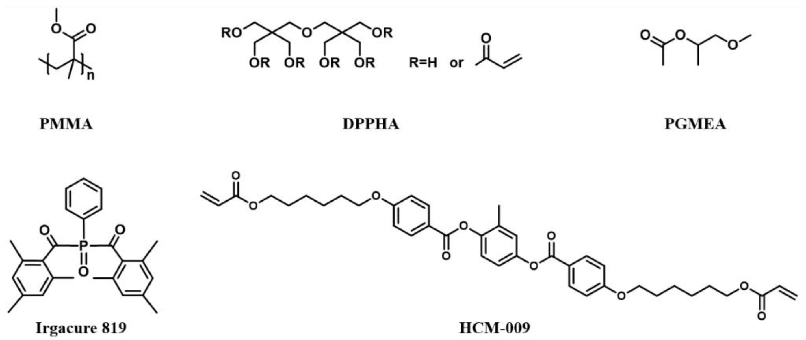
2.1. Materials
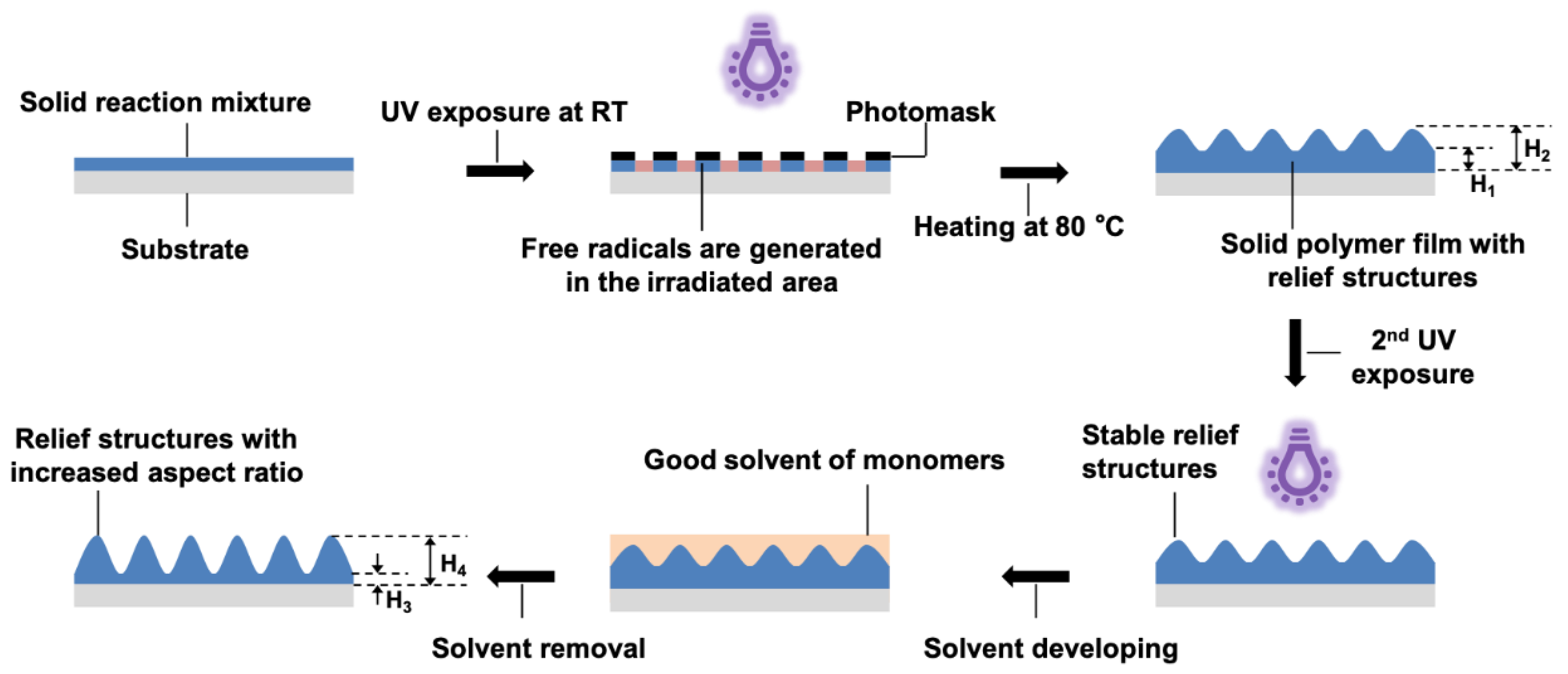
2.2. Preparation of Photo-Embossed Structures
2.3. Characterization
3. Results and Discussion
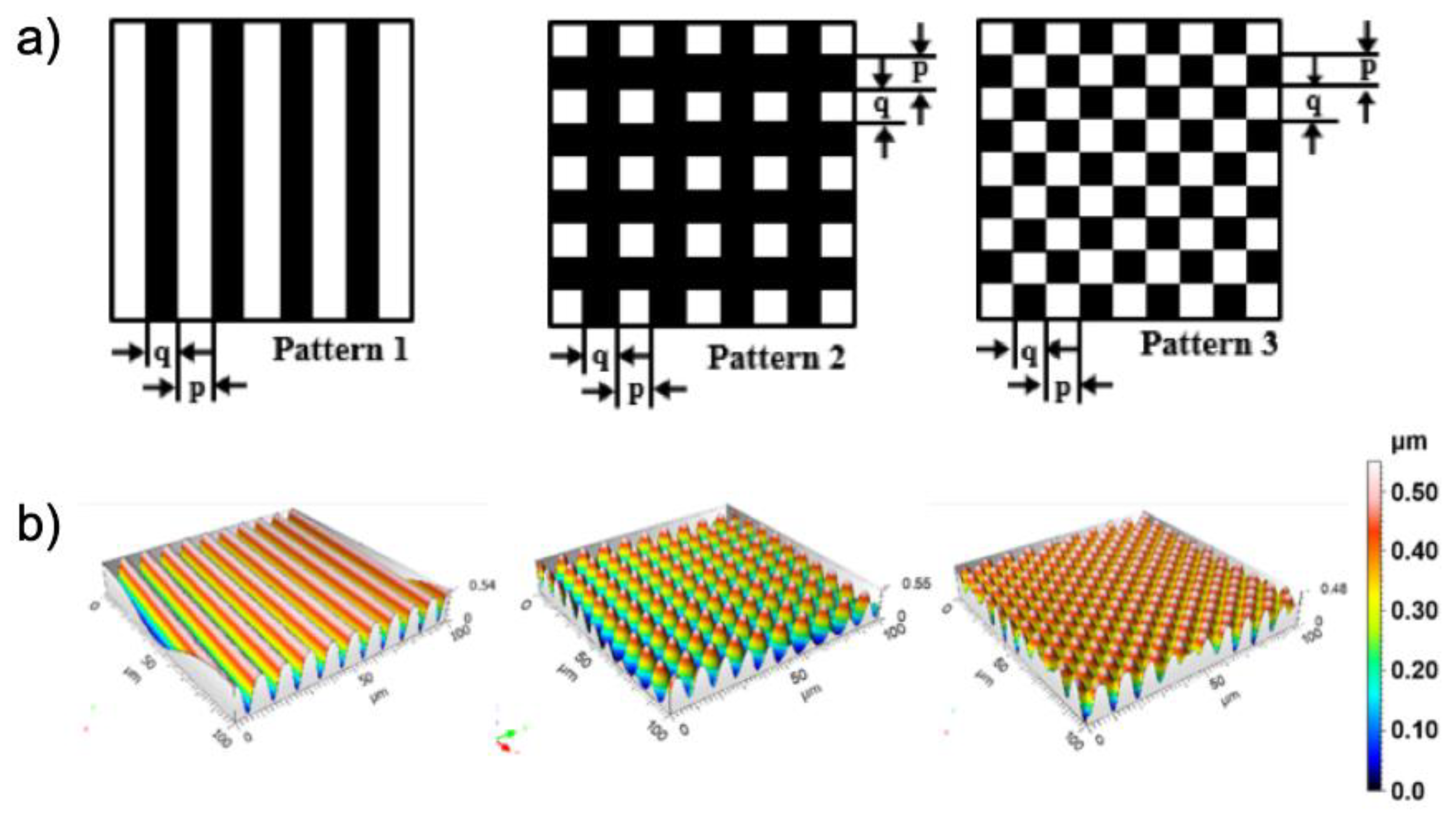
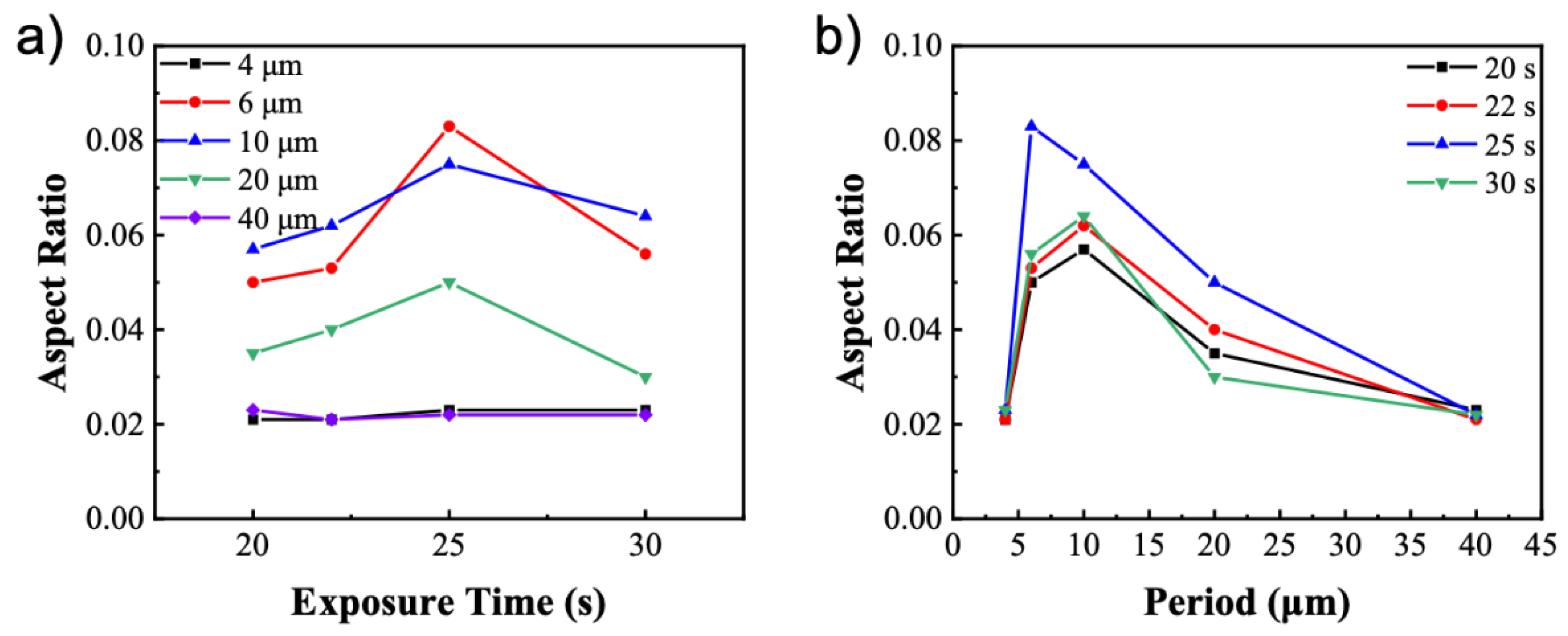
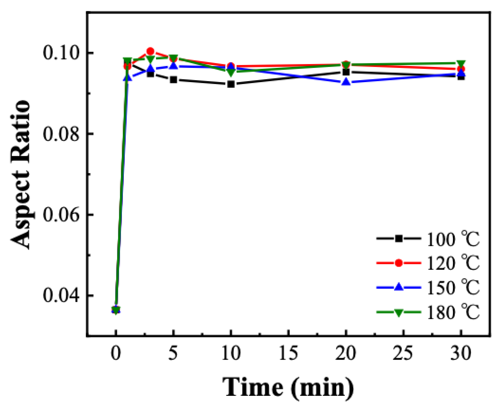
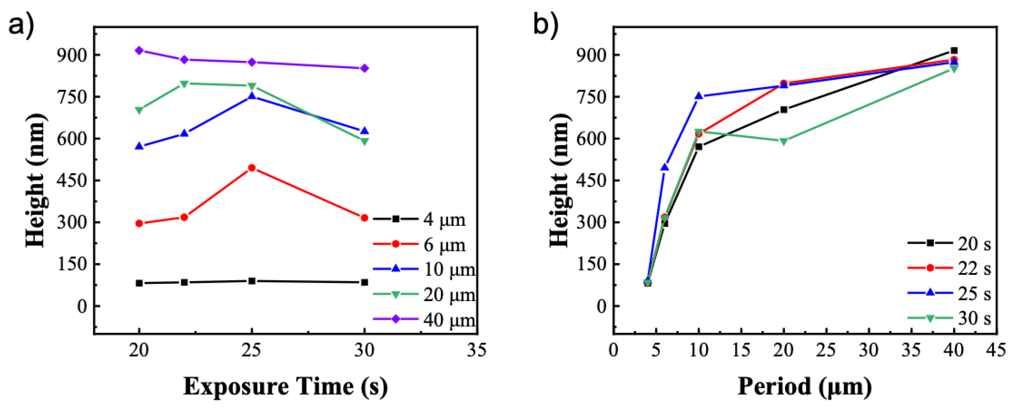
3.1. Photo-Embossed Surface Relief Structures with Improved Aspect Ratios
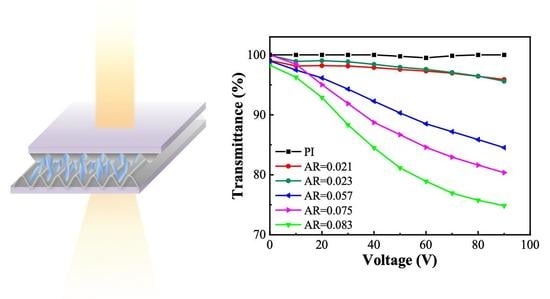
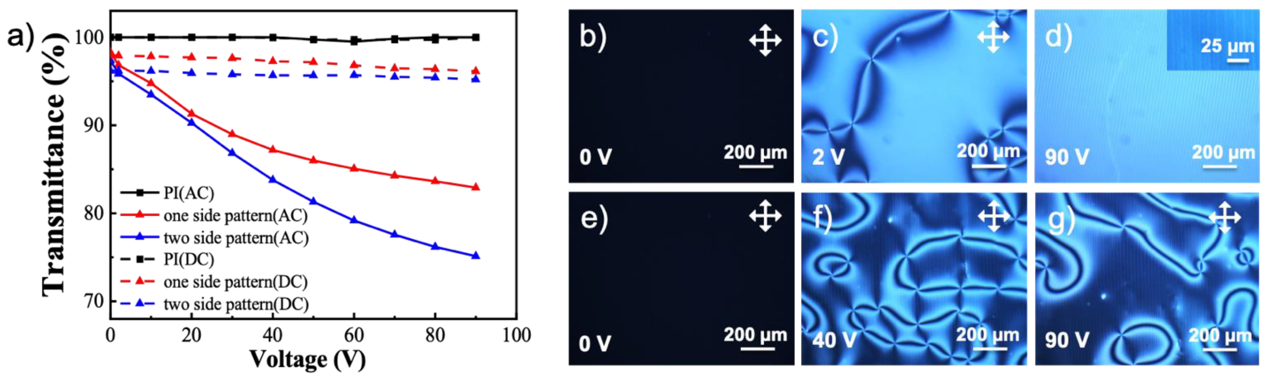
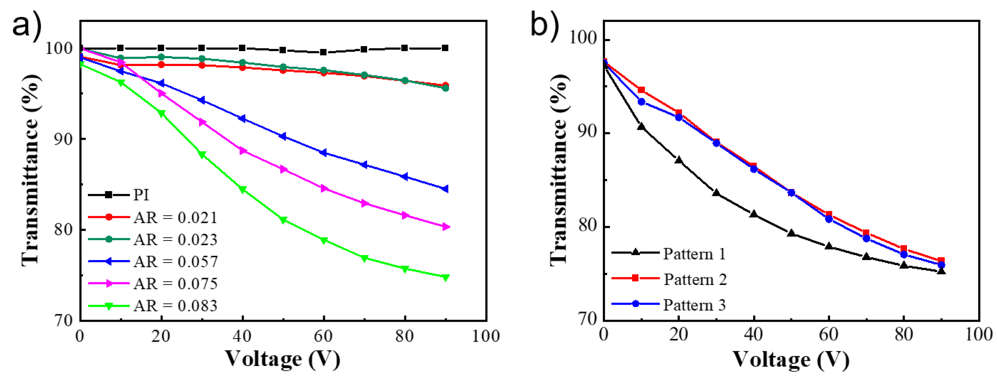
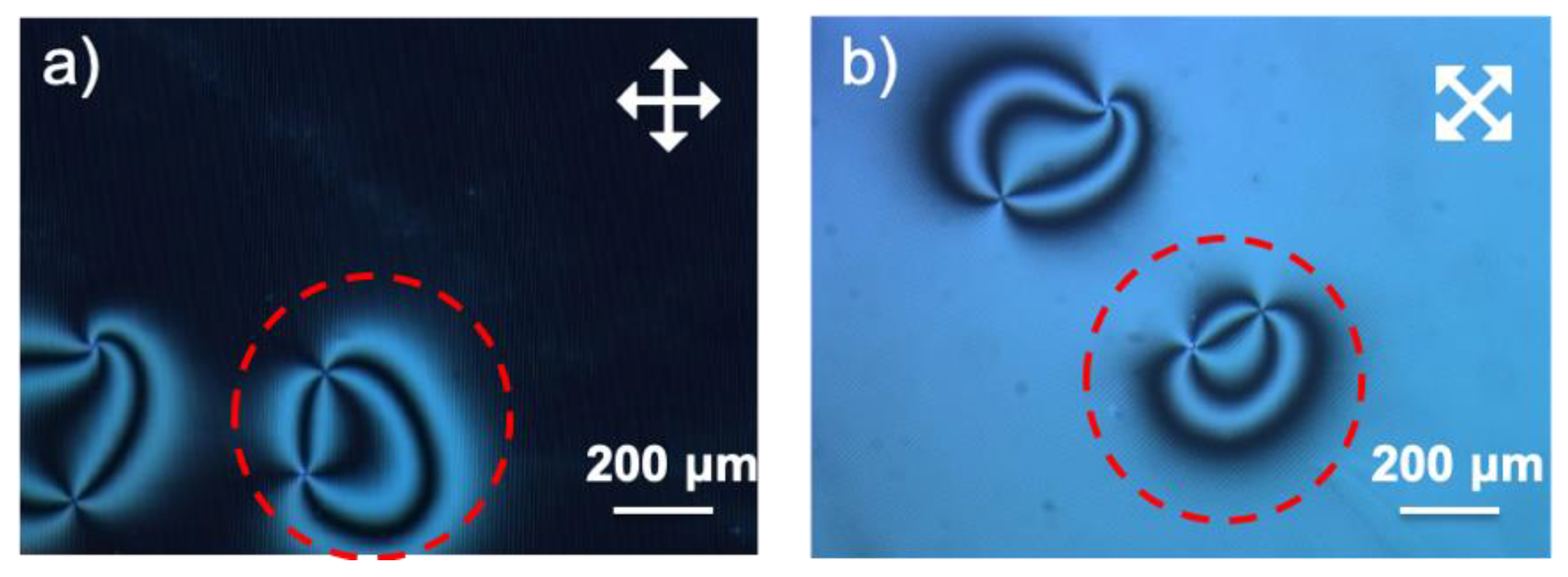
3.2. Liquid Crystal Devices Based on Photo-Embossed Surface Relief Structures
4. Conclusions
Author Contributions
Funding
Institutional Review Board Statement
Informed Consent Statement
Data Availability Statement
Acknowledgments
Conflicts of Interest
Appendix A


| Pattern | H1/H2 | Aspect Ratio | H3/H4 | New Aspect Ratio |
|---|---|---|---|---|
| #1 | 2.3/2.6 | 0.03 | 1.5/2.5 | 0.10 |
| #2 | 3.0/3.3 | 0.03 | 2.8/3.4 | 0.06 |
| #3 | 3.2/3.4 | 0.02 | 2.9/3.4 | 0.05 |
| Sample ID | H1/H2 | Aspect Ratio | H3/H4 | New Aspect Ratio |
|---|---|---|---|---|
| D | 2.3/2.6 | 0.03 | 1.5/2.5 | 0.10 |
| E | 4.5/4.9 | 0.04 | 3.7/4.8 | 0.11 |
| F | 2.2/2.7 | 0.05 | 1.3/2.6 | 0.13 |
| Pattern | Structure Height before Coating of PI (nm) | Structure Height after Coating of PI (nm) |
|---|---|---|
| #1 | 299 ± 8 | 552 ± 48 |
| #2 | 200 ± 6 | 524 ± 12 |
| #3 | 321 ± 18 | 523 ± 13 |
References
- Kim, Y.-K.; Wang, X.; Mondkar, P.; Bukusoglu, E.; Abbott, N.L. Self-Reporting and Self-Regulating Liquid Crystals. Nature 2018, 557, 539–544. [Google Scholar] [CrossRef] [PubMed]
- Wang, L.; Urbas, A.M.; Li, Q. Nature-Inspired Emerging Chiral Liquid Crystal Nanostructures: From Molecular Self-Assembly to DNA Mesophase and Nanocolloids. Adv. Mater. 2020, 32, 1801335. [Google Scholar] [CrossRef] [PubMed]
- Herbert, K.M.; Fowler, H.E.; McCracken, J.M.; Schlafmann, K.R.; Koch, J.A.; White, T.J. Synthesis and Alignment of Liquid Crystalline Elastomers. Nat. Rev. Mater. 2021, 1–16. [Google Scholar] [CrossRef]
- Zhao, W.; de Haan, L.T.; Broer, D.J.; Zhang, Y.; Lv, P.; Zhou, G. Photopolymerization-Enforced Stratification in Liquid Crystal Materials. Prog. Polym. Sci. 2021, 114, 101365. [Google Scholar] [CrossRef]
- Lee, B.; Clark, N.A. Alignment of Liquid Crystals with Patterned Isotropic Surfaces. Science 2001, 291, 2576–2580. [Google Scholar] [CrossRef] [PubMed]
- Kim, J.-H.; Yoneya, M.; Yokoyama, H. Tristable Nematic Liquid-Crystal Device Using Micropatterned Surface Alignment. Nature 2002, 420, 159–162. [Google Scholar] [CrossRef]
- Choi, M.C.; Pfohl, T.; Wen, Z.; Li, Y.; Kim, M.W.; Israelachvili, J.N.; Safinya, C.R. Ordered Patterns of Liquid Crystal Toroidal Defects by Microchannel Confinement. Proc. Natl. Acad. Sci. USA 2004, 101, 17340–17344. [Google Scholar] [CrossRef] [PubMed] [Green Version]
- Xia, Y.; Honglawan, A.; Yang, S. Tailoring Surface Patterns to Direct the Assembly of Liquid Crystalline Materials. Liq. Cryst. Rev. 2019, 7, 30–59. [Google Scholar] [CrossRef]
- Zhu, J.-C.; Han, T.; Guo, Y.; Wang, P.; Xie, H.-L.; Meng, Z.-G.; Yu, Z.-Q.; Tang, B.Z. Design and Synthesis of Luminescent Liquid Crystalline Polymers with “Jacketing” Effect and Luminescent Patterning Applications. Macromolecules 2019, 52, 3668–3679. [Google Scholar] [CrossRef]
- Honglawan, A.; Beller, D.A.; Cavallaro, M.; Kamien, R.D.; Stebe, K.J.; Yang, S. Pillar-Assisted Epitaxial Assembly of Toric Focal Conic Domains of Smectic-A Liquid Crystals. Adv. Mater. 2011, 23, 5519–5523. [Google Scholar] [CrossRef]
- Honglawan, A.; Beller, D.A.; Cavallaro, M.; Kamien, R.D.; Stebe, K.J.; Yang, S. Topographically Induced Hierarchical Assembly and Geometrical Transformation of Focal Conic Domain Arrays in Smectic Liquid Crystals. Proc. Natl. Acad. Sci. USA 2013, 110, 34–39. [Google Scholar] [CrossRef] [Green Version]
- Xia, Y.; Cedillo-Servin, G.; Kamien, R.D.; Yang, S. Guided Folding of Nematic Liquid Crystal Elastomer Sheets into 3D via Patterned 1D Microchannels. Adv. Mater. 2016, 28, 9637–9643. [Google Scholar] [CrossRef]
- Aharoni, H.; Xia, Y.; Zhang, X.; Kamien, R.D.; Yang, S. Universal Inverse Design of Surfaces with Thin Nematic Elastomer Sheets. Proc. Natl. Acad. Sci. USA 2018, 115, 7206–7211. [Google Scholar] [CrossRef] [PubMed] [Green Version]
- Abbott, N.L. Surface Effects on Orientation of Liquid Crystals. Curr. Opin. Colloid Interface Sci. 1997, 2, 76–82. [Google Scholar] [CrossRef]
- Yi, Y.; Nakata, M.; Martin, A.R.; Clark, N.A. Alignment of Liquid Crystals by Topographically Patterned Polymer Films Prepared by Nanoimprint Lithography. Appl. Phys. Lett. 2007, 90, 163510. [Google Scholar] [CrossRef]
- Lee, J.H.; Jeong, H.-C.; Won, J.; Oh, B.-Y.; Kim, D.H.; Lee, D.W.; Liu, Y.; Seo, D.-S. Nano Pattern Transfer on Acrylic Polymers with UV Irradiation for Liquid Crystal Alignment. Polymer 2019, 161, 1–7. [Google Scholar] [CrossRef]
- Jeong, H.-C.; Park, H.-G.; Lee, J.H.; Jang, S.B.; Oh, B.-Y.; Han, J.-M.; Seo, D.-S. Homogeneously Aligned Liquid Crystal Molecules on Reformed Poly(Methyl Methacrylate) via Ion-Beam Irradiation. Opt. Mater. 2016, 54, 288–293. [Google Scholar] [CrossRef]
- Lee, D.W.; Lee, J.H.; Kim, E.M.; Heo, G.S.; Kim, D.H.; Oh, J.Y.; Liu, Y.; Seo, D.-S. Surface Modification of a Poly(Ethylene-Co-Vinyl Acetate) Layer by Ion Beam Irradiation for the Uniform Alignment of Liquid Crystals. J. Mol. Liq. 2021, 339, 116700. [Google Scholar] [CrossRef]
- Lee, W.-K.; Choi, Y.S.; Kang, Y.-G.; Sung, J.; Seo, D.-S.; Park, C. Super-Fast Switching of Twisted Nematic Liquid Crystals on 2D Single Wall Carbon Nanotube Networks. Adv. Funct. Mater. 2011, 21, 3843–3850. [Google Scholar] [CrossRef]
- He, Z.; Tan, G.; Chanda, D.; Wu, S.-T. Novel Liquid Crystal Photonic Devices Enabled by Two-Photon Polymerization [Invited]. Opt. Express 2019, 27, 11472–11491. [Google Scholar] [CrossRef]
- Lv, P.; You, Y.; Li, J.; Zhang, Y.; Broer, D.J.; Chen, J.; Zhou, G.; Zhao, W.; Liu, D. Translating 2D Director Profile to 3D Topography in a Liquid Crystal Polymer. Adv. Sci. 2021, 8, 2004749. [Google Scholar] [CrossRef]
- Serra, F.; Gharbi, M.A.; Luo, Y.; Liu, I.B.; Bade, N.D.; Kamien, R.D.; Yang, S.; Stebe, K.J. Curvature-Driven, One-Step Assembly of Reconfigurable Smectic Liquid Crystal “Compound Eye” Lenses. Adv. Opt. Mater. 2015, 3, 1287–1292. [Google Scholar] [CrossRef] [Green Version]
- Meng, C.; Tseng, M.C.; Tang, S.T.; Zhao, C.X.; Yeung, S.Y.; Kwok, H.S. Normally Transparent Smart Window with Haze Enhancement via Inhomogeneous Alignment Surface. Liq. Cryst. 2019, 46, 484–491. [Google Scholar] [CrossRef]
- Moujdi, S.; Rahmouni, A.; Mahfoud, T.; Nesterenko, D.V.; Halim, M.; Sekkat, Z. Surface Relief Gratings in Azo-Polymers Revisited. J. Appl. Phys. 2018, 124, 213103. [Google Scholar] [CrossRef]
- Sekkat, Z. Optical Tweezing by Photomigration. Appl. Opt. 2016, 55, 259–268. [Google Scholar] [CrossRef]
- Sánchez, C.; de Gans, B.-J.; Kozodaev, D.; Alexeev, A.; Escuti, M.J.; van Heesch, C.; Bel, T.; Schubert, U.S.; Bastiaansen, C.W.M.; Broer, D.J. Photoembossing of Periodic Relief Structures Using Polymerization- Induced Diffusion: A Combinatorial Study. Adv. Mater. 2005, 17, 2567–2571. [Google Scholar] [CrossRef]
- Hermans, K.; Wolf, F.K.; Perelaer, J.; Janssen, R.A.J.; Schubert, U.S.; Bastiaansen, C.W.M.; Broer, D.J. High Aspect Ratio Surface Relief Structures by Photoembossing. Appl. Phys. Lett. 2007, 91, 174103. [Google Scholar] [CrossRef] [Green Version]
- Perelaer, J.; Hermans, K.; Bastiaansen, C.W.M.; Broer, D.J.; Schubert, U.S. Photo-Embossed Surface Relief Structures with an Increased Aspect Ratios by Addition of a Reversible Addition-Fragmentation Chain Transfer Agent. Adv. Mater. 2008, 20, 3117–3121. [Google Scholar] [CrossRef]
- Hermans, K.; Tomatsu, I.; Matecki, M.; Sijbesma, R.P.; Bastiaansen, C.W.M.; Broer, D.J. Highly Efficient Surface Relief Formation via Photoembossing of a Supramolecular Polymer. Macromol. Chem. Phys. 2008, 209, 2094–2099. [Google Scholar] [CrossRef]
- Liedtke, A.; Lei, C.; O’Neill, M.; Dyer, P.E.; Kitney, S.P.; Kelly, S.M. One-Step Photoembossing for Submicrometer Surface Relief Structures in Liquid Crystal Semiconductors. ACS Nano 2010, 4, 3248–3253. [Google Scholar] [CrossRef]
- Hughes-Brittain, N.F.; Picot, O.T.; Dai, M.; Peijs, T.; Bastiaansen, C.W.M. Effect of Polymer Binder on Surface Texturing by Photoembossing. Appl. Surf. Sci. 2012, 258, 8609–8612. [Google Scholar] [CrossRef]
- Kommeren, S.; Sullivan, T.; Bastiaansen, C.W.M. Tunable Surface Topography in Fluoropolymers Using Photo-Embossing. RSC Adv. 2016, 6, 69117–69123. [Google Scholar] [CrossRef] [Green Version]
- Dai, M.; Picot, O.T.; Hughes-Brittain, N.F.; Peijs, T.; Bastiaansen, C.W.M. Formation of Relief Structures on Fibres by Photo-Embossing. J. Mater. Chem. 2011, 21, 15527–15531. [Google Scholar] [CrossRef]
- Hughes-Brittain, N.F.; Qiu, L.; Picot, O.T.; Wang, W.; Peijs, T.; Bastiaansen, C.W.M. Surface Texturing of Electrospun Fibres by Photoembossing Using Pulsed Laser Interference Holography and Its Effects on Endothelial Cell Adhesion. Polymer 2017, 125, 40–49. [Google Scholar] [CrossRef]
- Hughes-Brittain, N.F.; Qiu, L.; Wang, W.; Peijs, T.; Bastiaansen, C.W.M. Photoembossing of Surface Relief Structures in Polymer Films for Biomedical Applications. J. Biomed. Mater. Res. Part B Appl. Biomater. 2014, 102, 214–220. [Google Scholar] [CrossRef] [PubMed]
- Martínez, A.; González-Lana, S.; Asín, L.; de la Fuente, J.M.; Bastiaansen, C.W.M.; Broer, D.J.; Sánchez-Somolinos, C. Nano-Second Laser Interference Photoembossed Microstructures for Enhanced Cell Alignment. Polymers 2021, 13, 2958. [Google Scholar] [CrossRef] [PubMed]
- Zhang, Y.; Wang, C.; Zhao, W.; Li, M.; Wang, X.; Yang, X.; Hu, X.; Yuan, D.; Yang, W.; Zhang, Y.; et al. Polymer Stabilized Liquid Crystal Smart Window with Flexible Substrates Based on Low-Temperature Treatment of Polyamide Acid Technology. Polymers 2019, 11, 1869. [Google Scholar] [CrossRef] [PubMed] [Green Version]
- Adams, N.; De Gans, B.-J.; Kozodaev, D.; Sánchez, C.; Bastiaansen, C.W.M.; Broer, D.J.; Schubert, U.S. High-Throughput Screening and Optimization of Photoembossed Relief Structures. J. Comb. Chem. 2006, 8, 184–191. [Google Scholar] [CrossRef]
- De Gans, B.-J.; Sánchez, C.; Kozodaev, D.; Wouters, D.; Alexeev, A.; Escuti, M.J.; Bastiaansen, C.W.M.; Broer, D.J.; Schubert, U.S. Optimizing Photo-Embossed Gratings: A Gradient Library Approach. J. Comb. Chem. 2006, 8, 228–236. [Google Scholar] [CrossRef]


| Sample ID | Experimental Conditions | H1/H2 | Aspect Ratio | H3/H4 | New Aspect Ratio |
|---|---|---|---|---|---|
| Z (control) | No solvent developing step | 2.3/2.6 | 0.03 | -- | -- |
| A |
| 2.3/2.6 | 0.03 | 1.9/2.5 | 0.06 |
| B |
| 2.3/2.6 | 0.03 | 2.3/2.6 | 0.03 |
| C |
| 2.4/2.7 | 0.03 | 1.8/2.6 | 0.08 |
| D |
| 2.3/2.6 | 0.03 | 1.5/2.5 | 0.10 |
Publisher’s Note: MDPI stays neutral with regard to jurisdictional claims in published maps and institutional affiliations. |
© 2022 by the authors. Licensee MDPI, Basel, Switzerland. This article is an open access article distributed under the terms and conditions of the Creative Commons Attribution (CC BY) license (https://creativecommons.org/licenses/by/4.0/).
Share and Cite
Yang, X.; Gu, M.; Wei, Q.; Zhang, Y.; Wu, S.; Wu, Q.; Hu, X.; Zhao, W.; Zhou, G. Photo-Embossed Surface Relief Structures with Improved Aspect Ratios and Their Applications in Liquid Crystal Devices. Polymers 2022, 14, 171. https://0-doi-org.brum.beds.ac.uk/10.3390/polym14010171
Yang X, Gu M, Wei Q, Zhang Y, Wu S, Wu Q, Hu X, Zhao W, Zhou G. Photo-Embossed Surface Relief Structures with Improved Aspect Ratios and Their Applications in Liquid Crystal Devices. Polymers. 2022; 14(1):171. https://0-doi-org.brum.beds.ac.uk/10.3390/polym14010171
Chicago/Turabian StyleYang, Xiulan, Minzhao Gu, Qunmei Wei, Yang Zhang, Sihan Wu, Qin Wu, Xiaowen Hu, Wei Zhao, and Guofu Zhou. 2022. "Photo-Embossed Surface Relief Structures with Improved Aspect Ratios and Their Applications in Liquid Crystal Devices" Polymers 14, no. 1: 171. https://0-doi-org.brum.beds.ac.uk/10.3390/polym14010171