
Implementation of Microwave Circuits Using Stereolithography

 ,
,  , and
, and 
Abstract
:1. Introduction
2. Materials and Methods
2.1. Resin
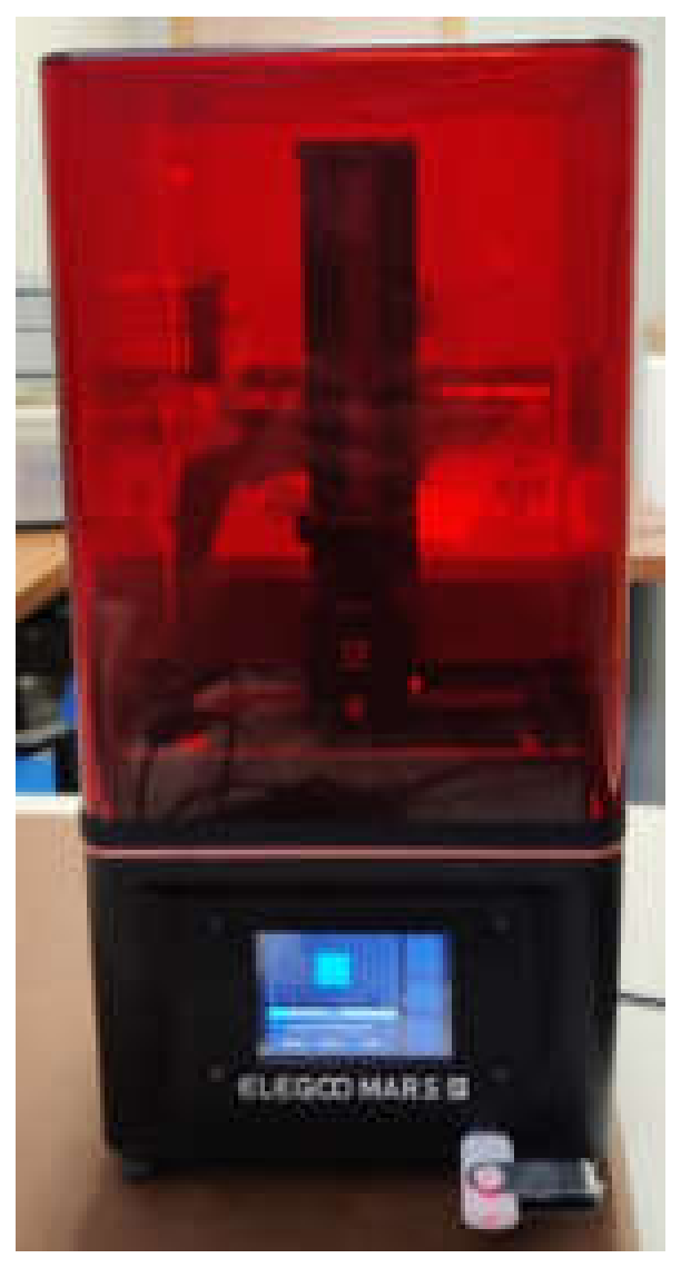
2.2. 3D Printer
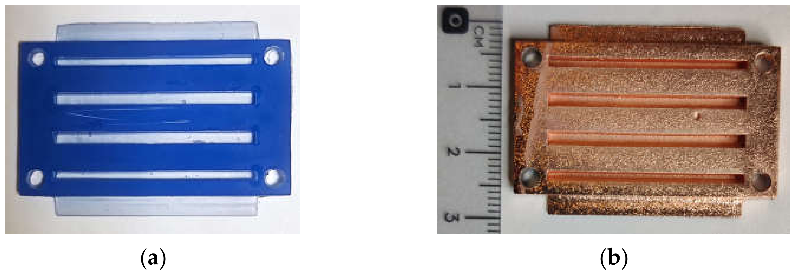
2.3. Manufacturing Process
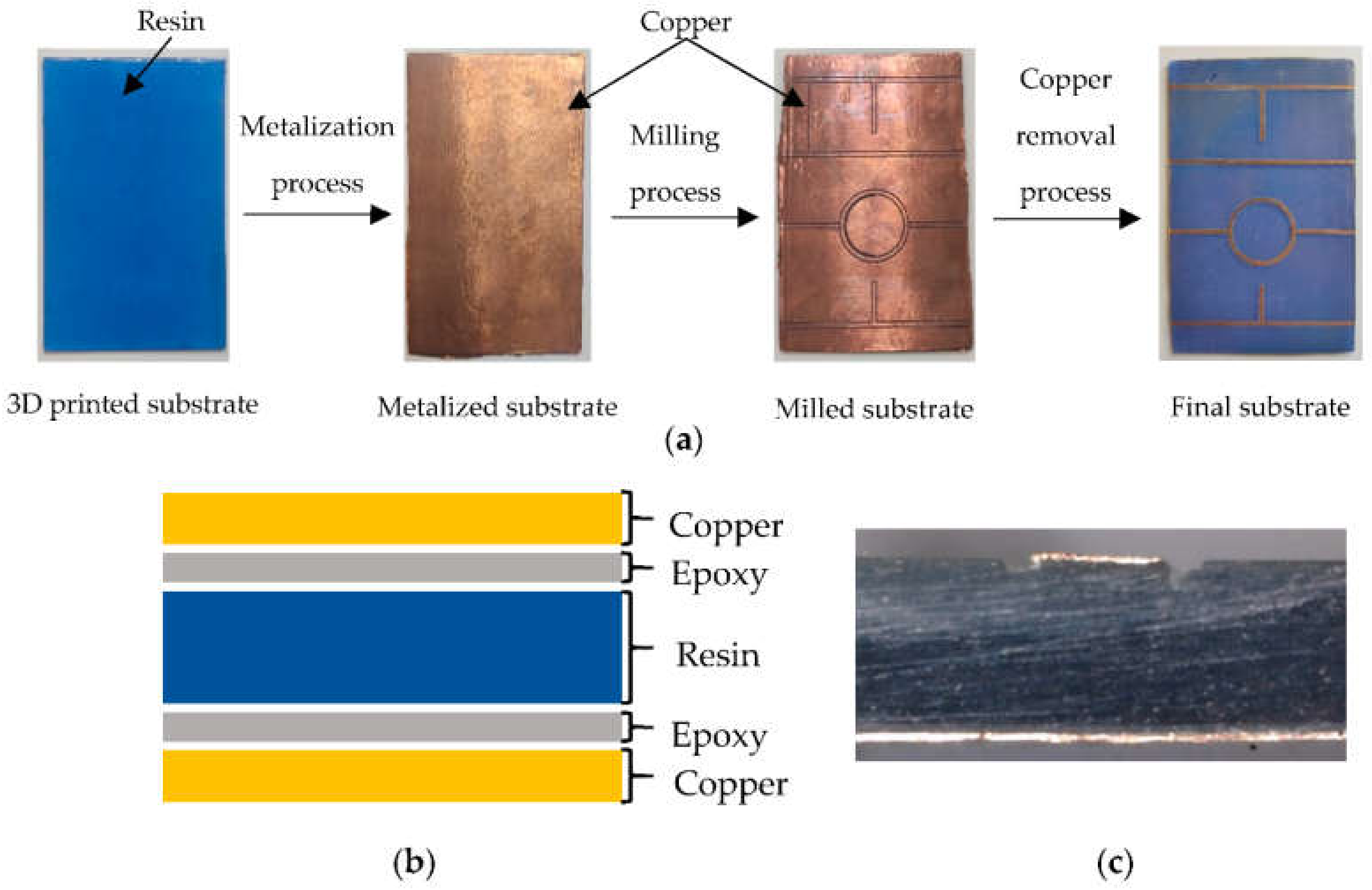
2.3.1. Substrate Metallization Using a Glued Copper Layer
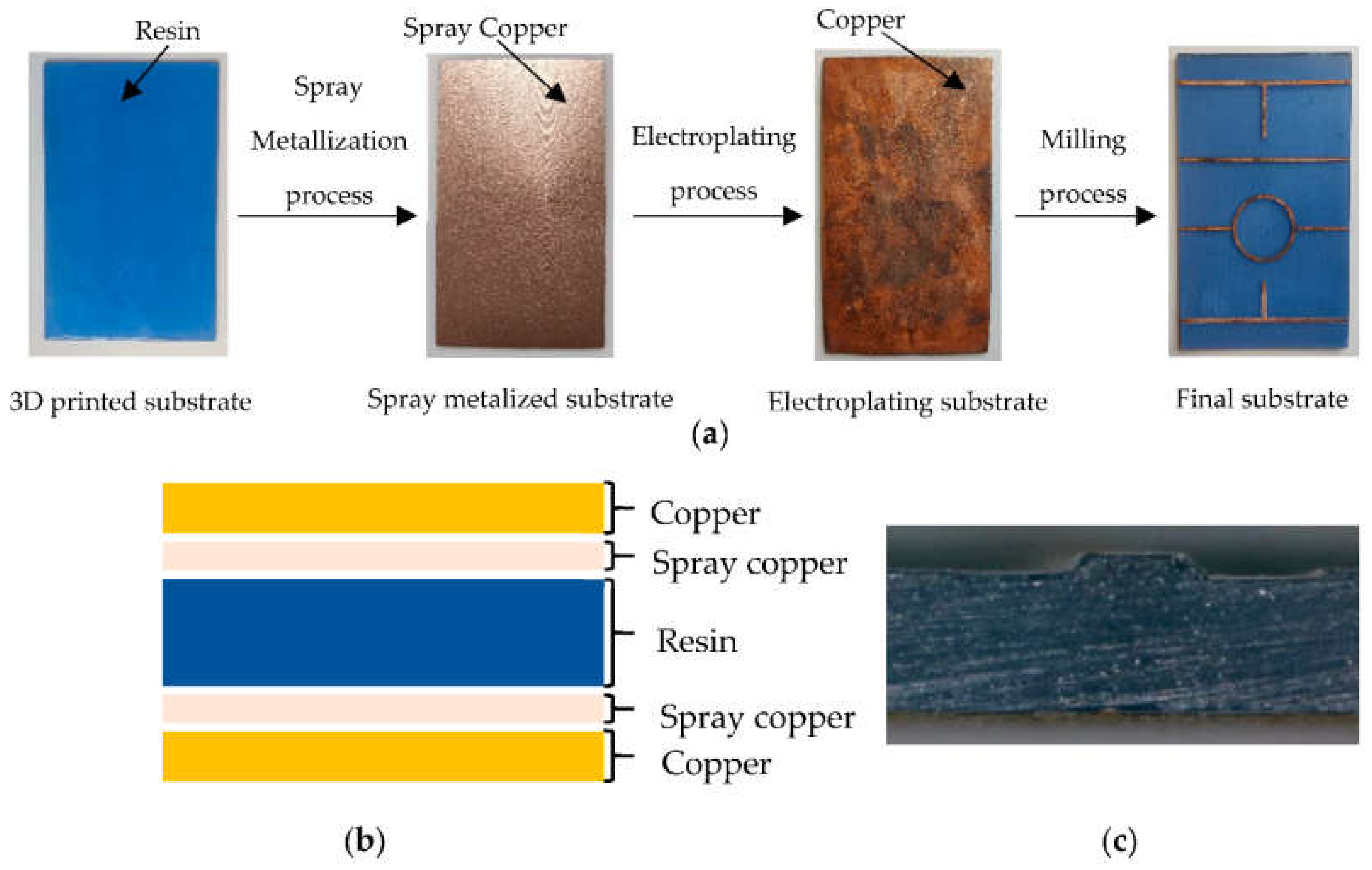
2.3.2. Substrate Metallization Using Copper Spray Paint and Electroplating
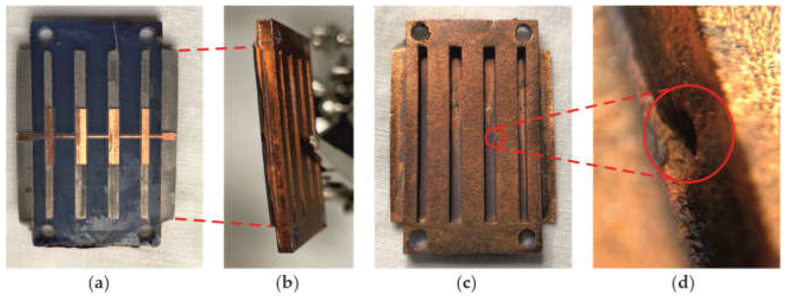
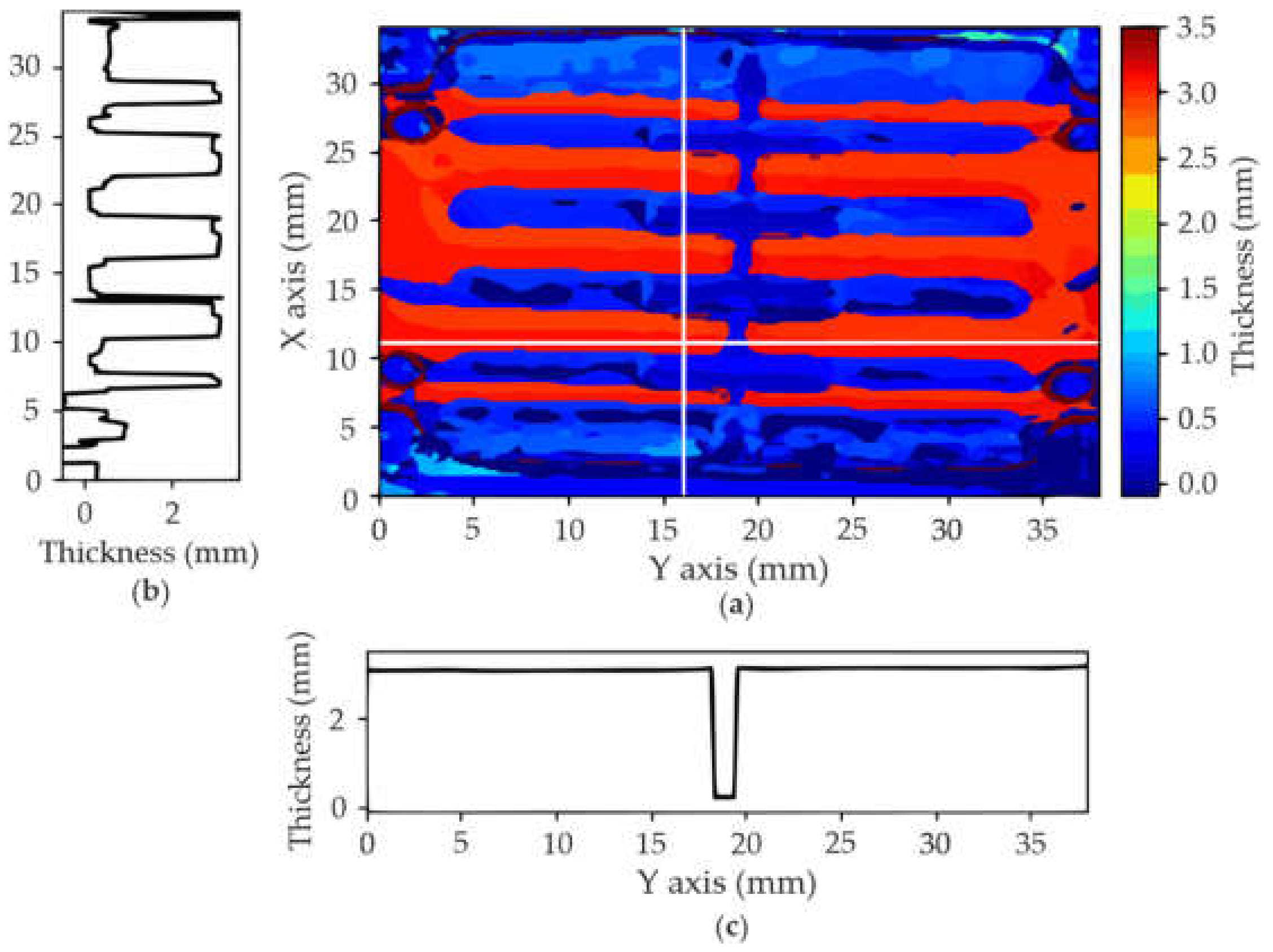
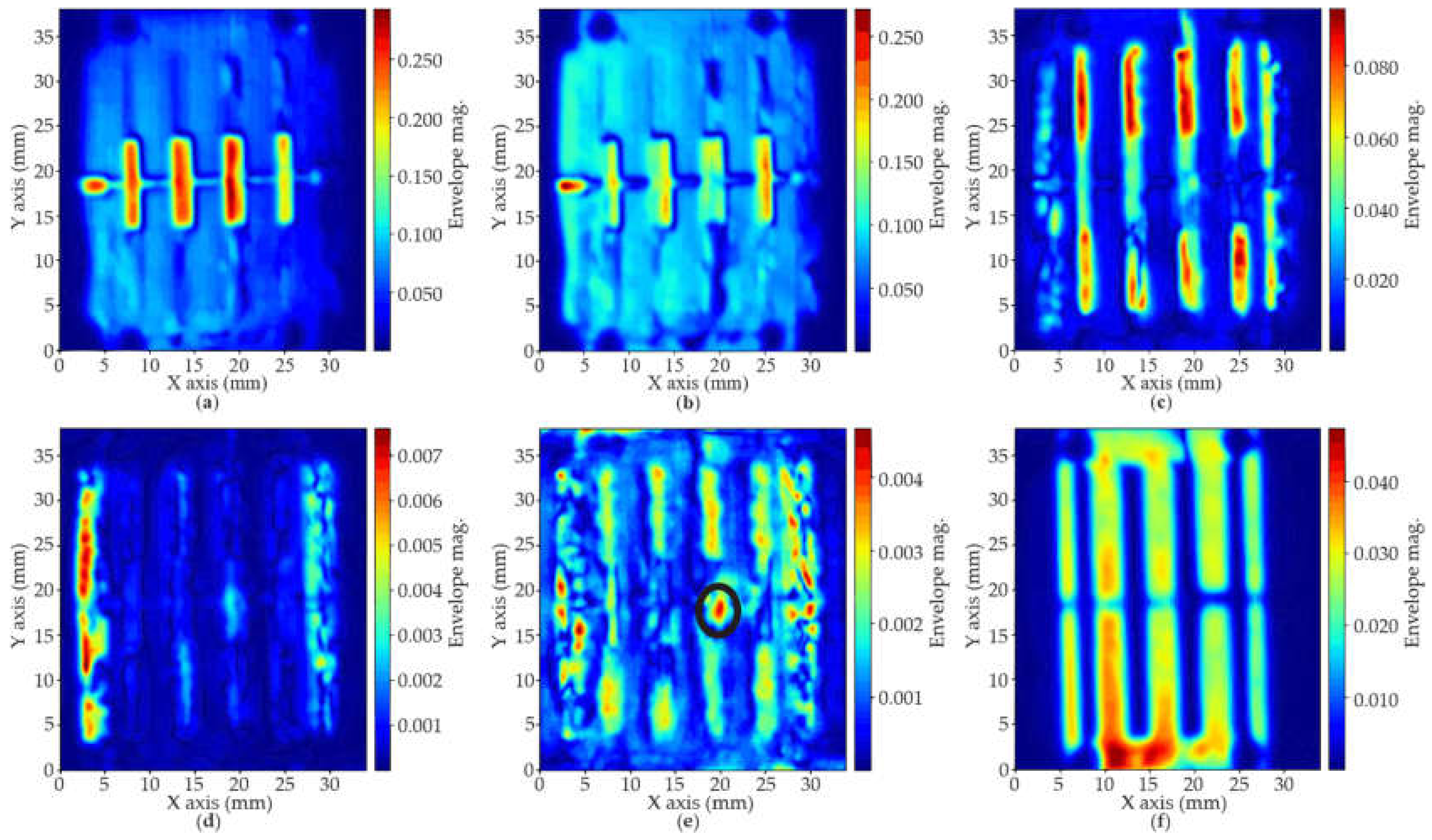
2.4. Structural Analysis
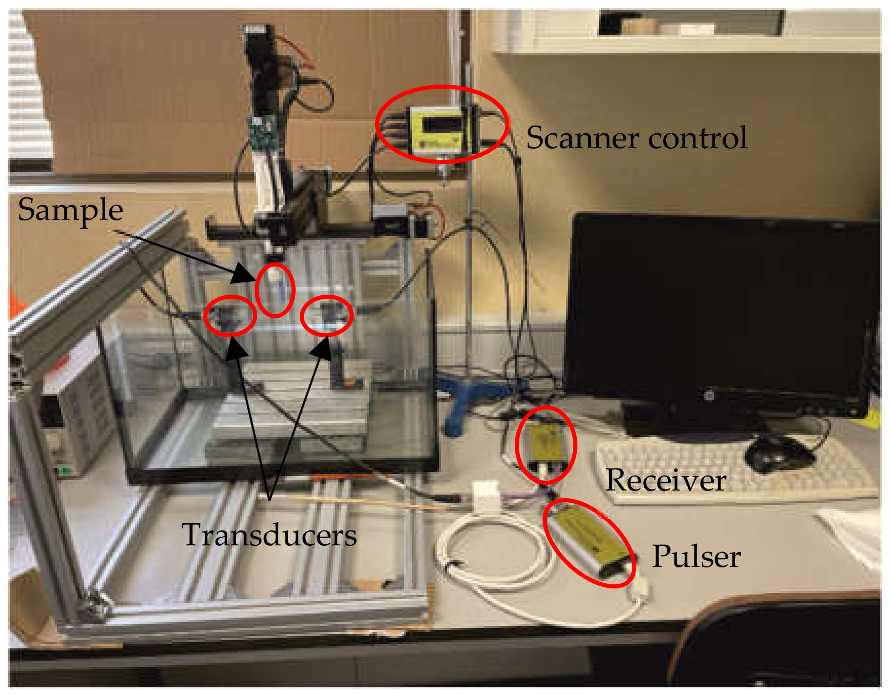
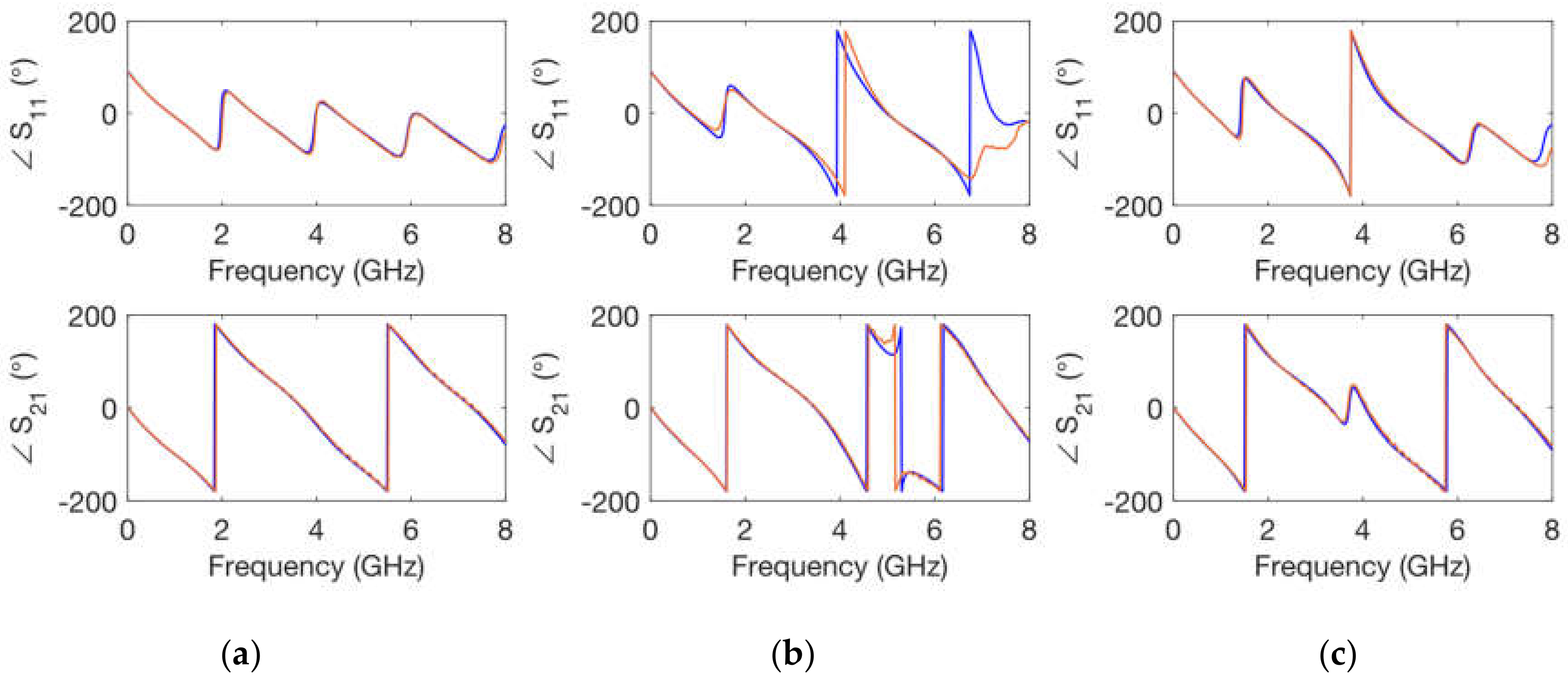
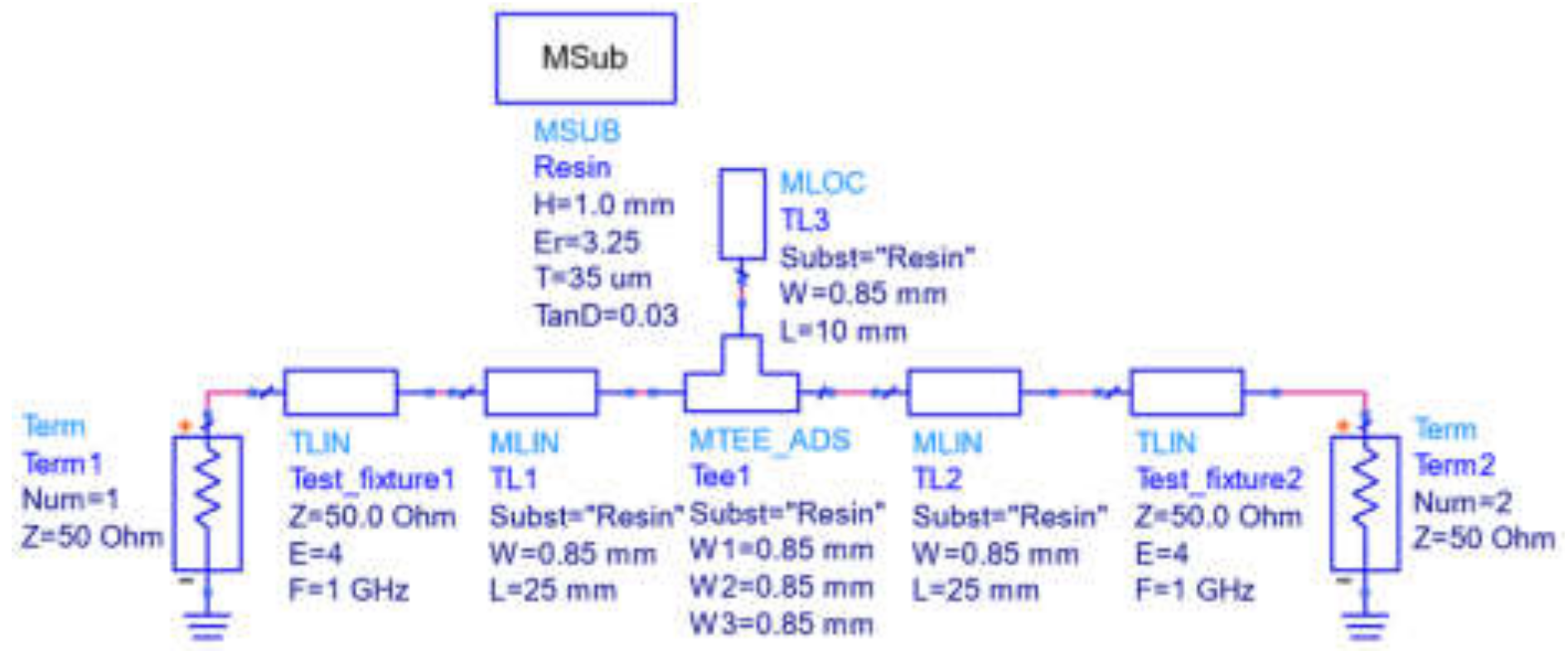
2.5. Electrical Characterization at Microwave Frequencies
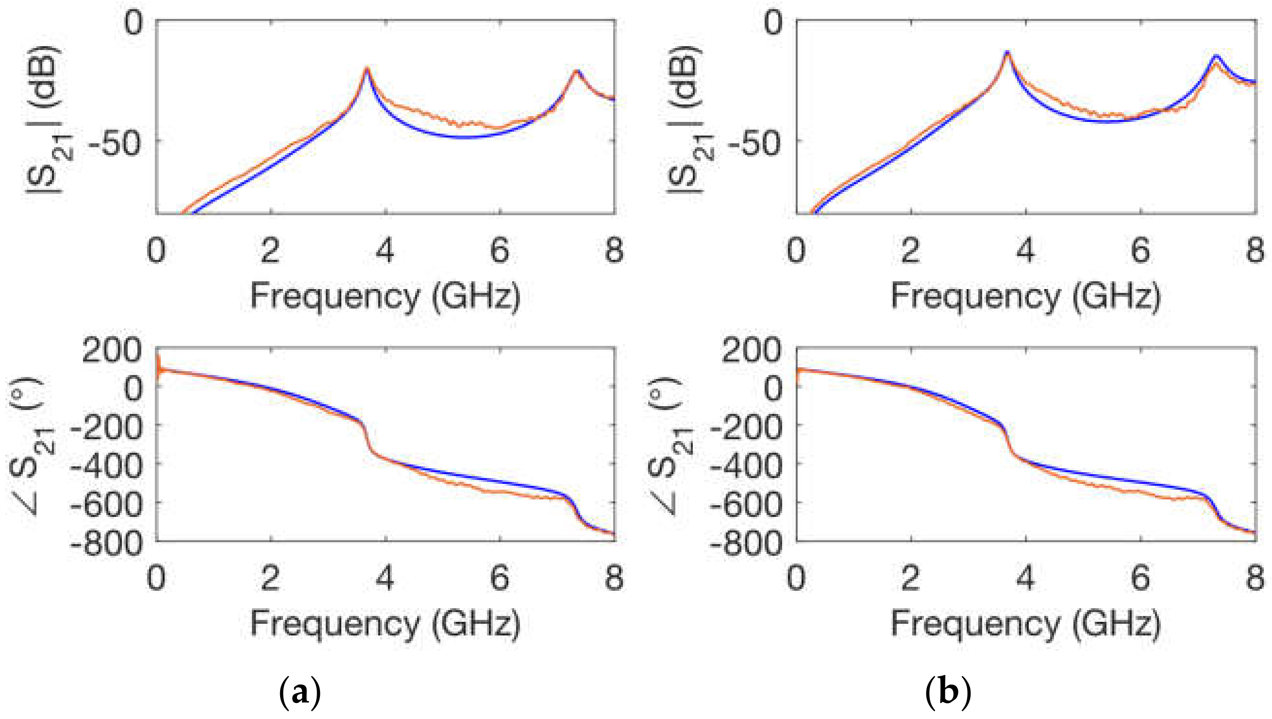
2.5.1. Glued Copper Layer Metallization
2.5.2. Resin Substrate Metallization Using Electroplating
3. Results
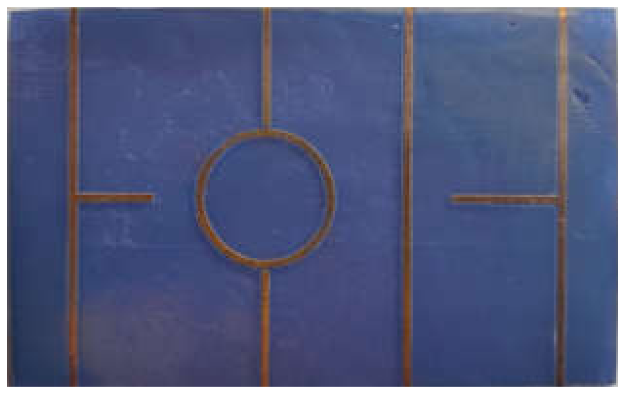
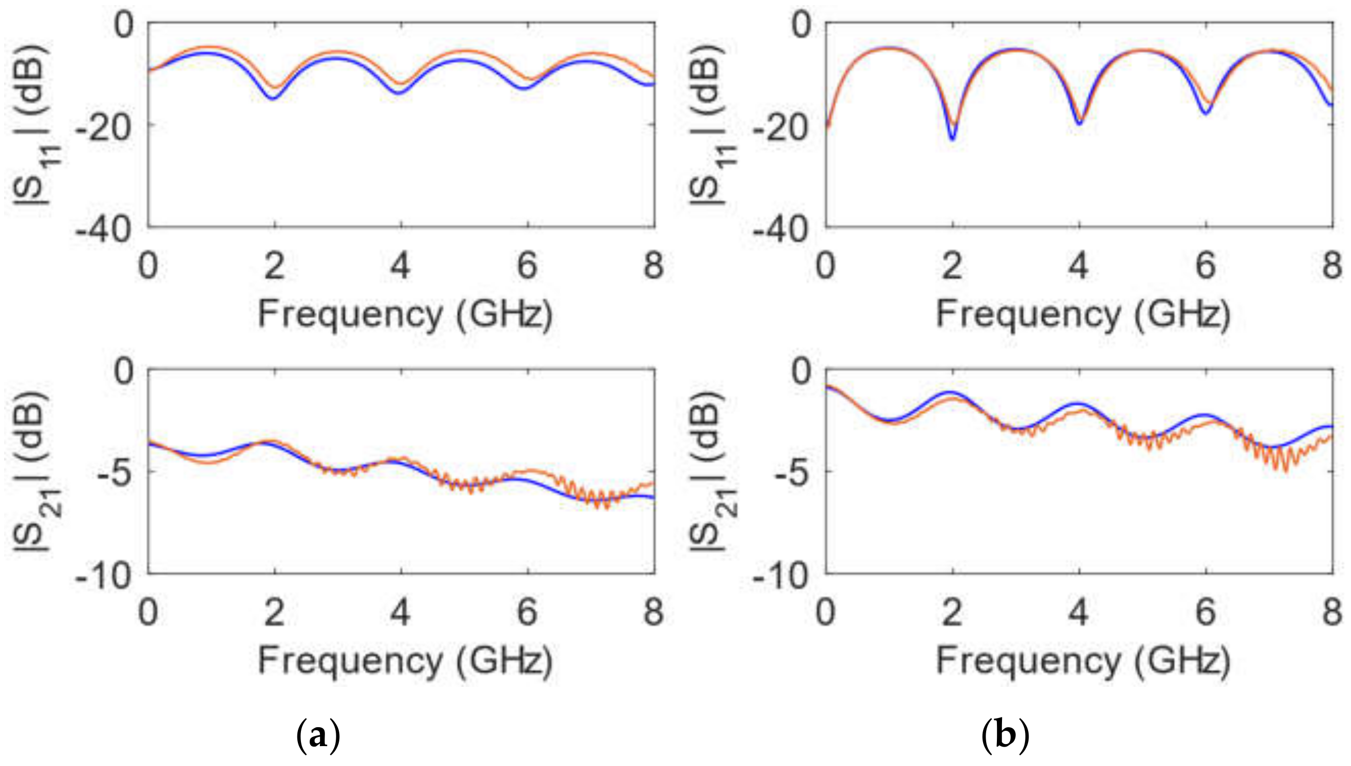
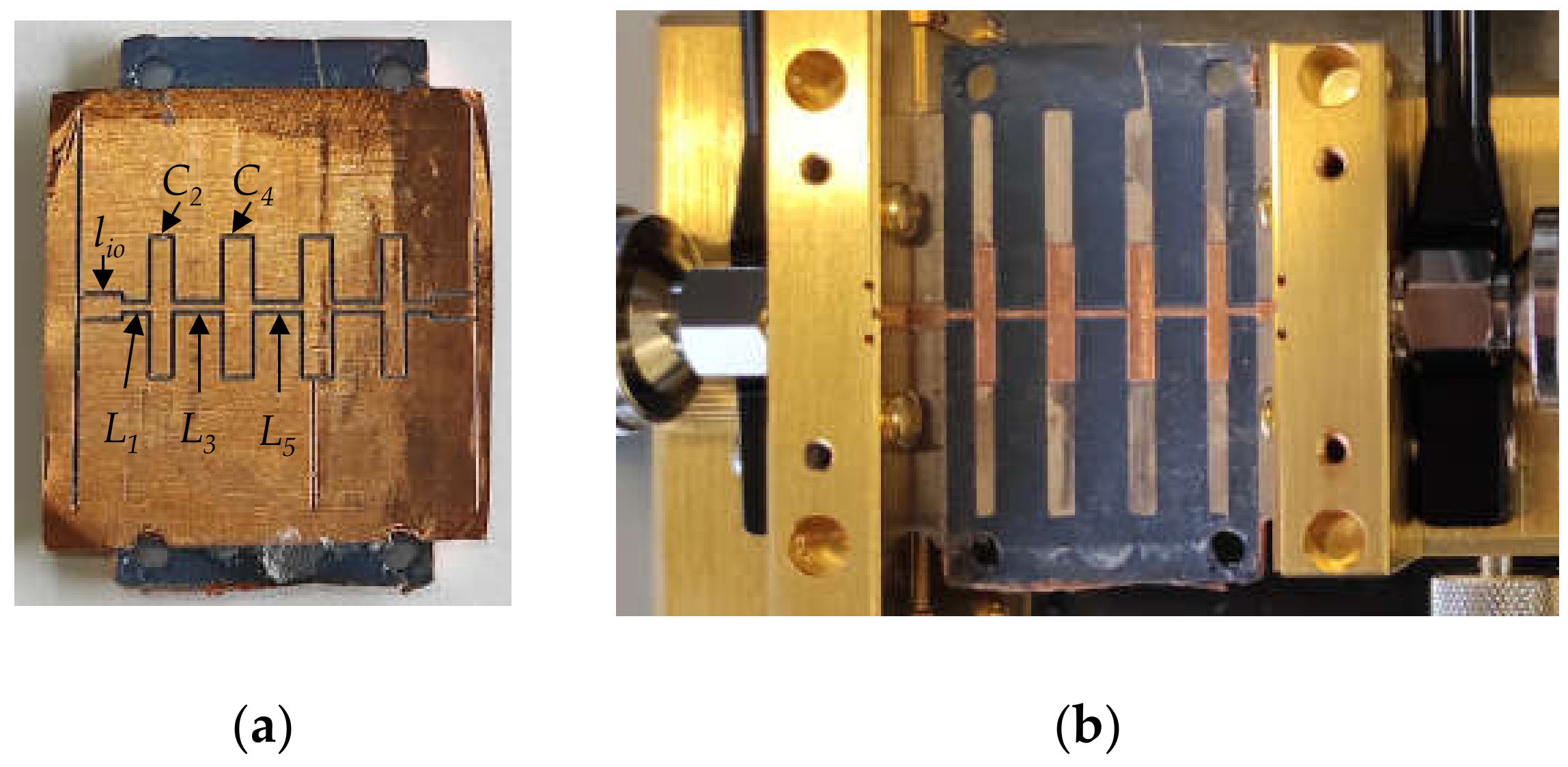
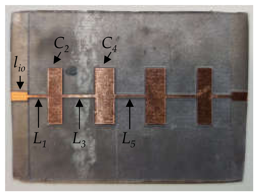
3.1. Filter Design
3.2. Filter Structural Analysis
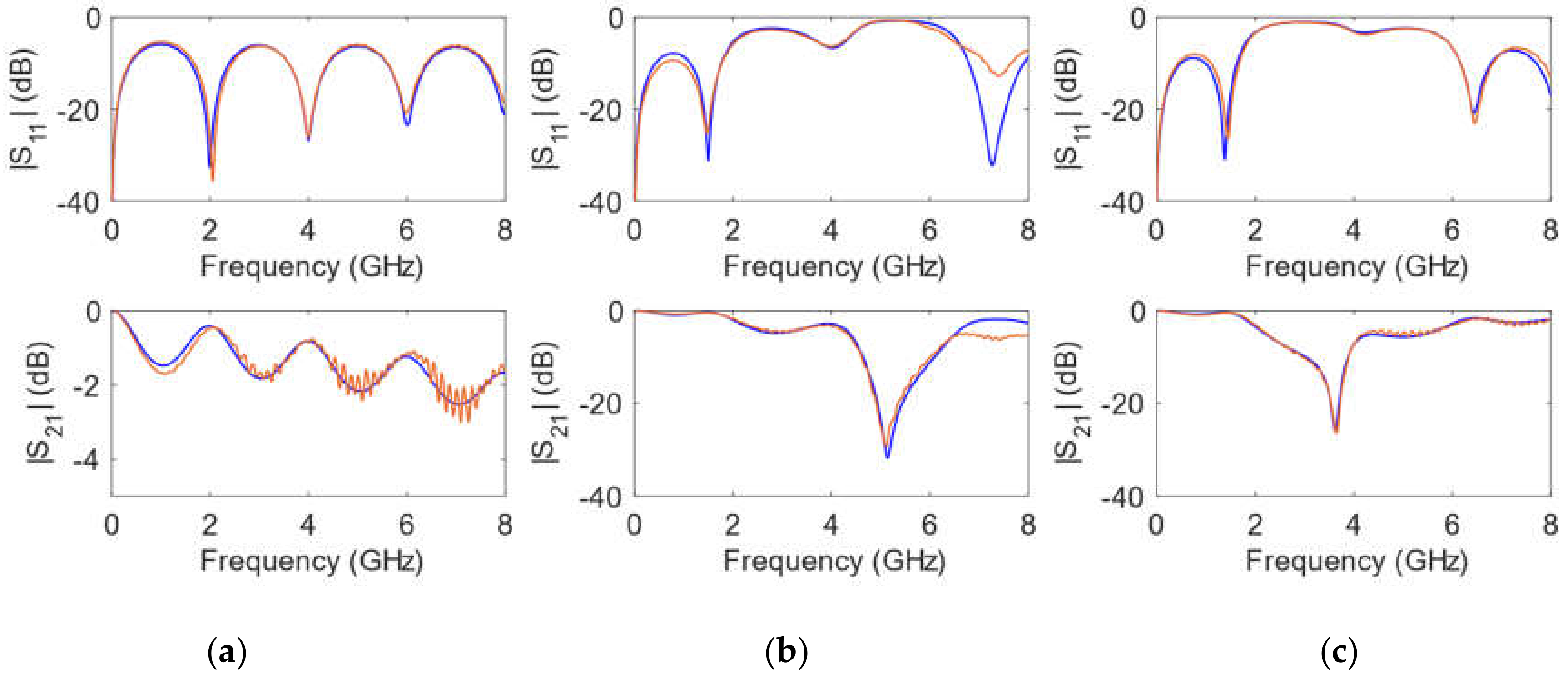
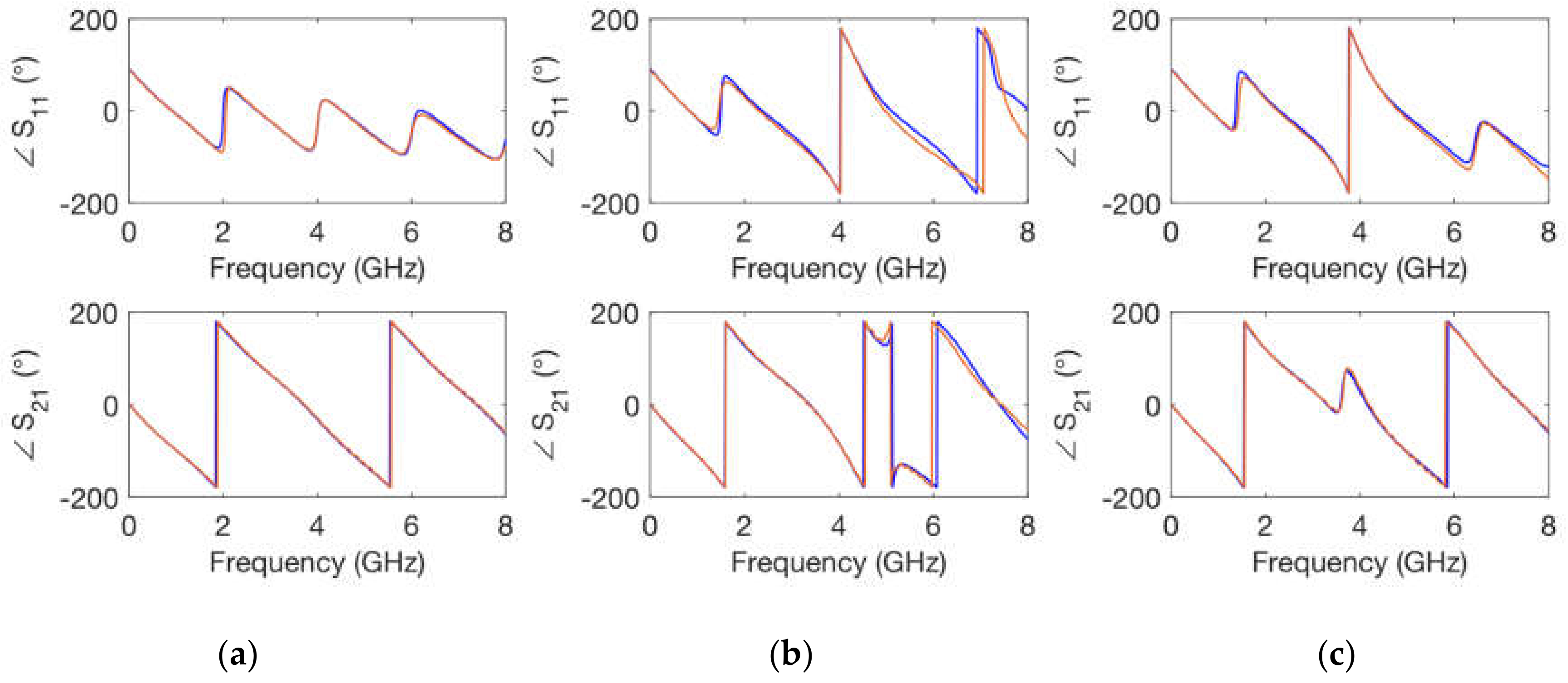
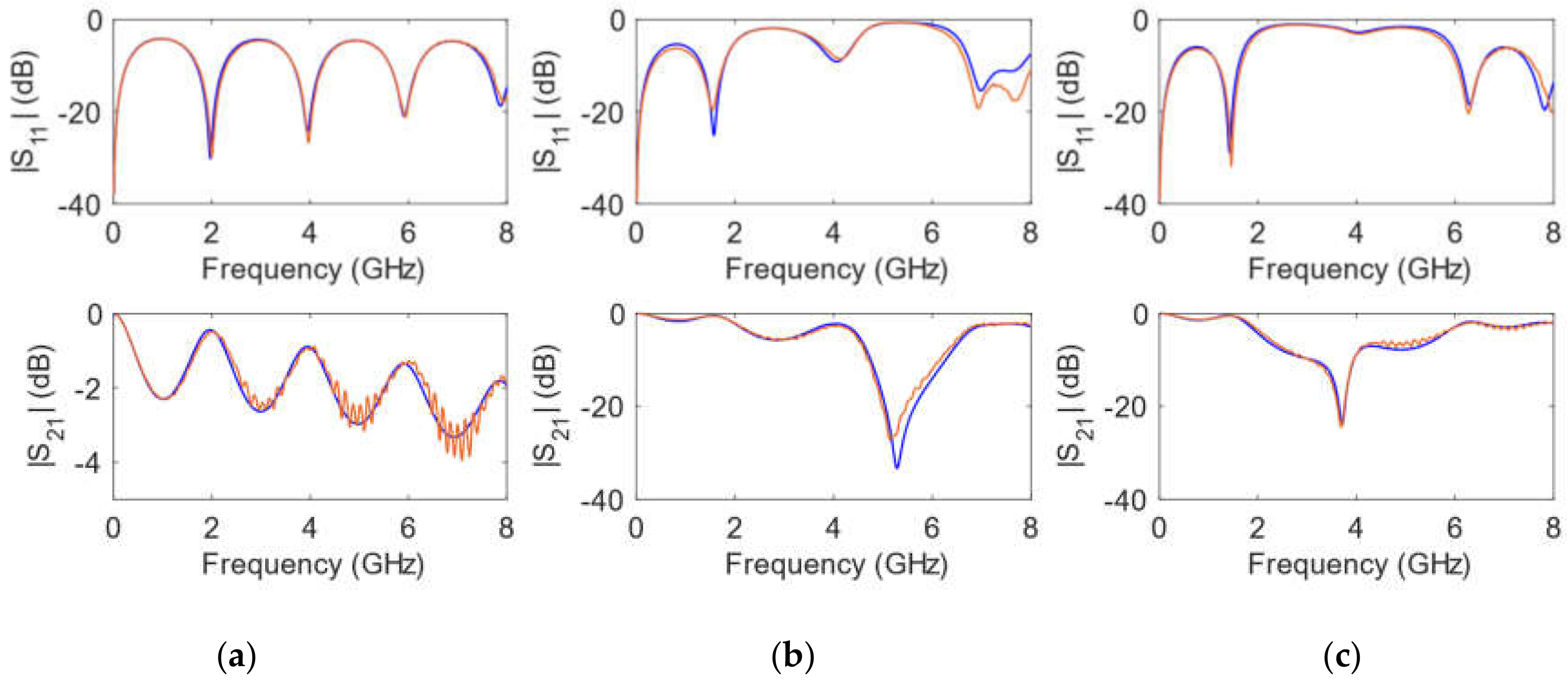
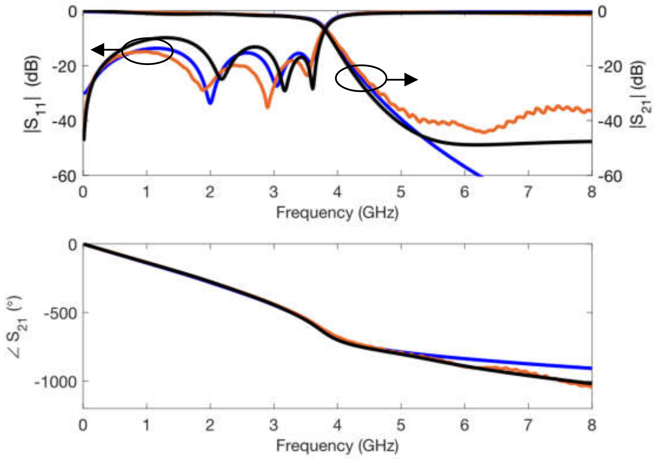
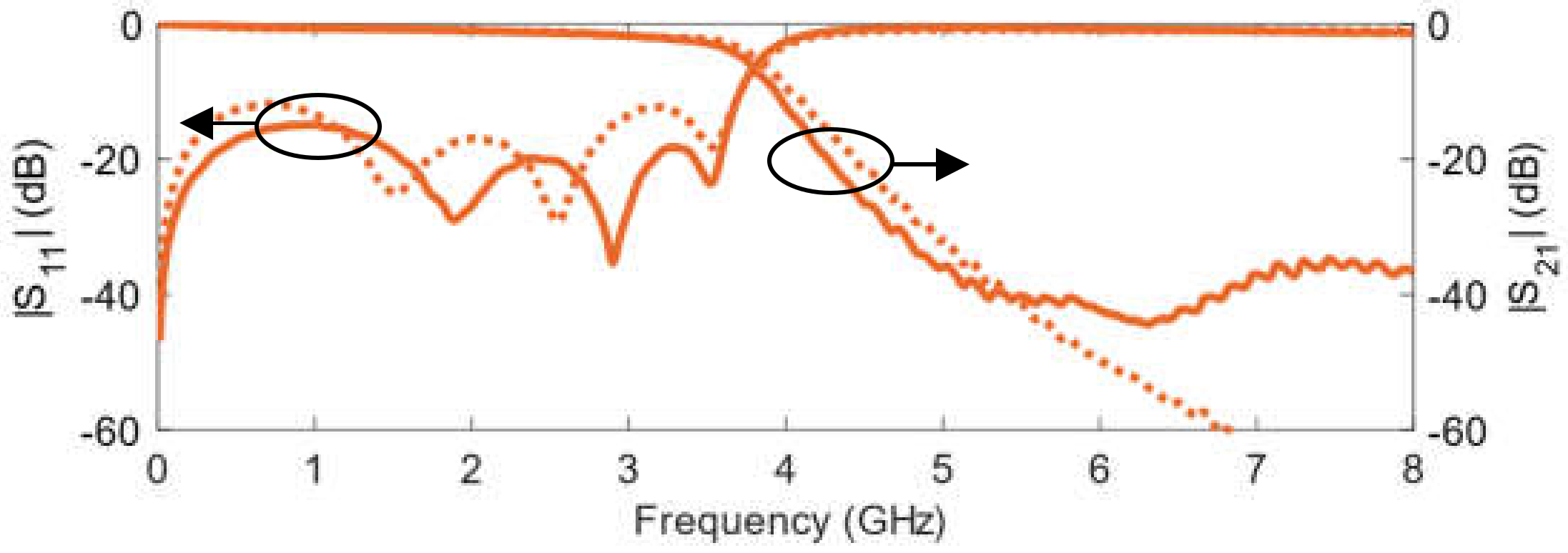
3.3. Filter Electrical Response
4. Conclusions
Author Contributions
Funding
Institutional Review Board Statement
Informed Consent Statement
Data Availability Statement
Conflicts of Interest
References
- Sing, S.L.; An, J.; Yeong, W.Y.; Wiria, F.E. Laser and electron-beam powder-bed additive manufacturing of metallic implants: A review on processes, materials and designs. J. Orthop. Res. 2016, 34, 369–385. [Google Scholar] [CrossRef] [PubMed]
- Zhu, C.; Li, T.; Mohideen, M.M.; Hu, P.; Gupta, R.; Ramakrishna, S.; Liu, Y. Realization of circular economy of 3D printed plastics: A review. Polymers 2021, 13, 744. [Google Scholar] [CrossRef] [PubMed]
- Bandyopadhyay, A.; Bose, S. Additive Manufacturing; CRC Press: Boca Raton, FL, USA, 2016. [Google Scholar]
- Srivatsan, T.; Sudarshan, T. Additive Manufacturing: Innovations, Advances, and Applications; CRC Press: Boca Raton, FL, USA, 2015. [Google Scholar]
- Paolini, A.; Kollmannsberger, S.; Rank, E. Additive manufacturing in construction: A review on processes, applications, and digital planning methods. Addit. Manuf. 2019, 30, 100894. [Google Scholar] [CrossRef]
- Burton, H.E.; Peel, S.; Eggbeer, D. Reporting fidelity in the literature for computer aided design and additive manufacture of implants and guides. Addit. Manuf. 2018, 23, 362–373. [Google Scholar] [CrossRef]
- Kestilä, A.; Nordling, K.; Miikkulainen, V.; Kaipio, M.; Tikka, T.; Salmi, M.; Auer, A.; Leskelä, M.; Ritala, M. Towards space-grade 3D-printed, ALD-coated small satellite propulsion components for fluidics. Addit. Manuf. 2018, 22, 31–37. [Google Scholar] [CrossRef]
- Roulon, S.; Soulairol, I.; Cazes, M.; Lemierre, L.; Payre, N.; Delbreilh, L.; Alié, J. D-Sorbitol Physical Properties Effects on Filaments Used by 3D Printing Process for Personalized Medicine. Molecules 2021, 26, 3000. [Google Scholar] [CrossRef]
- Rojas-Nastrucci, A.; Nussbaum, J.T.; Crane, N.B.; Weller, T.M. Ka-Band characterization of binder jetting for 3-D printing of metallic rectangular waveguide circuits and antennas. IEEE Trans. Microw. Theory Tech. 2017, 65, 3099–3108. [Google Scholar] [CrossRef]
- Dahle, R.; Laforge, P.; Kuhling, J. 3-D printed customizable insert for waveguide filter design at X-Band. IEEE Microw. Wirel. Compon. Lett. 2017, 27, 1080–1082. [Google Scholar] [CrossRef]
- Rocco, G.M.; Bozzi, M.; Schreurs, D.; Perregrini, L.; Marconi, S.; Alaimo, G.; Auricchio, F. 3-D printed microfluidic sensor in SIW technology for liquids’ characterization. IEEE Trans. Microw. Theory Tech. 2020, 68, 1175–1184. [Google Scholar] [CrossRef]
- Lai, W.; Wang, Y.; He, J. Electromagnetic wave absorption properties of structural conductive ABS fabricated by fused deposition modeling. Polymers 2020, 12, 1217. [Google Scholar] [CrossRef]
- Zhang, B.; Guo, Y.-X.; Sun, H.; Wu, Y. Metallic, 3D-Printed, K-Band-Stepped, Double-Ridged Square Horn Antennas. Appl. Sci. 2018, 8, 33. [Google Scholar] [CrossRef] [Green Version]
- Helena, D.; Ramos, A.; Varum, T.; Matos, J.N. The Use of 3D Printing Technology for Manufacturing Metal Antennas in the 5G/IoT Context. Sensors 2021, 21, 3321. [Google Scholar] [CrossRef]
- Avşar Aydın, E. 3D-Printed Graphene-Based Bow-Tie Microstrip Antenna Design and Analysis for Ultra-Wideband Applications. Polymers 2021, 13, 3724. [Google Scholar] [CrossRef]
- Massoni, E.; Silvestri, L.; Alaimo, G.; Marconi, S.; Bozzi, M.; Perregrini, L.; Auricchio, F. 3-D printed substrate integrated slab waveguide for single-mode bandwidth enhancement. IEEE Microw. Wirel. Compon. Lett. 2017, 27, 536–538. [Google Scholar] [CrossRef]
- Rogers Corporation. Product Selector Guide. Available online: https://rogerscorp.com/-/media/project/rogerscorp/documents/advanced-electronics-solutions/english/product-selection-guides/acs-product-selector-guide-and-standard-thicknesses-and-tolerances.pdf (accessed on 15 January 2022).
- AGC Multi Material. Available online: https://www.agc-multimaterial.com/page/advanced-dielectric-division-product-comparison-table-65.html (accessed on 15 January 2022).
- García-Martínez, H.; Ávila-Navarro, E.; Torregrosa-Penalva, G.; Rodríguez-Martínez, A.; Blanco-Angulo, C.; de la Casa-Lillo, M. Low-Cost Additive Manufacturing Techniques Applied to the Design of Planar Microwave Circuits by Fused Deposition Modeling. Polymers 2020, 12, 1946. [Google Scholar] [CrossRef]
- Kim, Y.; Tentzeris, M.M.; Lim, S. Low-Loss and Light Substrate Integrated Waveguide Using 3D Printed Honeycomb Structure. Materials 2019, 12, 402. [Google Scholar] [CrossRef] [Green Version]
- García-Martinez, H.; Avila, E.; Torregrosa Penalva, G.; Bronchalo, E.; Blanco Angulo, C.; Bozzi, M. Multilayered additive-manufactured half-wavelength coupled line filters. Int. J. Electron. Commun. 2020, 123, 153320. [Google Scholar] [CrossRef]
- Kerekes, T.; Lim, H.; Yeol, W.; Jin, G. Characterization of process–deformation/damage property relationship of fused deposition modeling (FDM) 3D-printed specimens. Addit. Manuf. 2019, 25, 532–544. [Google Scholar]
- Ferretti, P.; Leon-Cardenas, C.; Santi, G.M.; Sali, M.; Ciotti, E.; Frizziero, L.; Donnici, G.; Liverani, A. Relationship between FDM 3D Printing Parameters Study: Parameter Optimization for Lower Defects. Polymers 2021, 13, 2190. [Google Scholar] [CrossRef]
- Basile, E.; Grande, M.; Marrocco, V.; Laneve, D.; Petrignani, S.; Prudenzano, F.; Fassi, I. Design and Manufacturing of Super-Shaped Dielectric Resonator Antennas for 5G Applications Using Stereolithography. IEEE Access 2020, 8, 82929–82937. [Google Scholar] [CrossRef]
- Melchiorre, L.; Marasco, I.; Niro, G.; Basile, V.; Marrocco, V.; D’Orazio, A.; Grande, M. Bio-Inspired Dielectric Resonator Antenna for Wideband Sub-6 GHz Range. Appl. Sci. 2020, 10, 8826. [Google Scholar] [CrossRef]
- Basile, V.; Marrocco, V.; Spina, M.; Fassi, I.; D’Orazio, A.; Grande, M. 3D Printed Micro-Cells for Phase Control in 5G mm Wave Applications. IEEE Access 2021, 9, 46049–46060. [Google Scholar] [CrossRef]
- Melentiev, R.; Yu, N.; Marrocco, V.; Lubineau, G. Polymer metallization via cold spray additive manufacturing: A review of process control, coating qualities, and prospective applications. Addit. Manuf. 2021, 48, 102459. [Google Scholar] [CrossRef]
- Ohiri, K.A.; Nowicki, N.M.; Montalbano, T.J.; Presley, M.; Lazarus, N.S. Electroplating of Aerosol Jet-Printed Silver Inks. Adv. Eng. Mater. 2021, 23, 2100362. [Google Scholar] [CrossRef]
- Eßbach, C.; Fischer, D.; Nickel, D. Challenges in electroplating of additive manufactured ABS plastics. J. Manuf. Processes 2021, 88, 1378–1386. [Google Scholar] [CrossRef]
- Lai, Z.; Zhao, T.; Zhu, P.; Xiang, J.; Liu, D.; Liang, X.; Sun, R. Directly Electroplated Metallization on Flexible Substrates Based on Silver Nanowire Conductive Composite for Wearable Electronics. ACS Appl. Nano Mater. 2021, 4, 12098–12107. [Google Scholar] [CrossRef]
- Salazar, R.; Pizarro, F.; Vasquez, D.; Rajo-Iglesias, E. Assessment of 3D-printed waveguides using conductive filaments and a chloroform-based smoothing process. Addit. Manuf. 2022, 51, 102593. [Google Scholar] [CrossRef]
- Rogers Corporation. Processing Guidelines for RO4400™ Bonding Layers. Available online: https://rogerscorp.com/-/media/project/rogerscorp/documents/advanced-connectivity-solutions/english/fabrication-information/fabrication-guidelines-ro4400-bonding-layers.pdf (accessed on 22 January 2022).
- García-Martinez, H.; Ávila-Navarro, E.; Torregrosa-Penalva, G.; Delmonte, N.; Silvestri, L.; Marconi, S.; Alaimo, G.; Auricchio, F.; Bozzi, M. Design and fabrication of a band-pass filter with EBG single-ridge waveguide using additive manufacturing techniques. IEEE Trans. Microw. Theory Tech. 2020, 68, 4361–4368. [Google Scholar] [CrossRef]
- Angel, K.; Tsang, H.; Bedair, S.; Smith, G.; Lazarus, N. Selective electroplating of 3D printed parts. Addit. Manuf. 2018, 20, 164–172. [Google Scholar] [CrossRef]
- Rodríguez, A.; Sivilainis, L.; Dumbrava, V.; Chaziachmetovas, A.; Salazar, A. Automatic simultaneous measurement of phase velocity and thickness in Composite plates using iterative deconvolution. NDT E Int. 2014, 66, 117–127. [Google Scholar] [CrossRef]
- Hirao, M.; Ogi, H.; Sato, K. Interface Delamination of Layered Media: Acoustic Spectroscopy and Modal Analysis. IEEE Trans. Ultrason. Ferroelectr. Freq. Control 2004, 51, 439–443. [Google Scholar] [CrossRef]
- Álvarez-Arenas, T.G. Simultaneous determination of the ultrasound velocity and the thickness of solid plates from the analysis of thickness resonances using air-coupled ultrasound. Ultrasonics 2010, 50, 104–109. [Google Scholar] [CrossRef]
- Livings, R.; Dayal, V.; Barnard, D. Damage detection in a multi-layered, multi-material composite using air-coupled ultrasonic resonance imaging. J. Nondestruct. Eval. 2016, 35, 55. [Google Scholar] [CrossRef]
- Hettler, J.; Tabatabaeipour, M.; Delrue, S.; Abeele, K.V.D. Detection and characterization of local defect resonances arising from delaminations and flat bottom holes. J. Nondestruct. Eval. 2017, 36, 2. [Google Scholar] [CrossRef]
- Castaings, M.; Siryabe, E.; Renier, M.; Meziane, A. Ultrasonic characterization of cohesive and adhesive properties of adhesive bonds. J. Acoust. Soc. Am. 2015, 138, 1766. [Google Scholar] [CrossRef]
- García-Martinez, H.; Torregrosa-Penalva, G.; Ávila-Navarro, E.; Coves-Soler, A.; Bronchalo, E. Complex Structures in Microwave Circuits by Using Additive Manufacturing Techniques. In Proceedings of the 49th European Microwave Conference (EuMC), Paris, France, 1–3 October 2019; pp. 782–785. [Google Scholar]
- 3D JAKE. Resin Basic. Available online: https://www.3djake.es/3djake/color-mix-resin-basic?sai=9430 (accessed on 24 January 2022).
- Elegoo. Elegoo Mars Pro. Available online: https://www.elegoo.com/collections/mars-series/products/elegoo-mars-pro-lcd-3d-printer (accessed on 20 January 2022).
- CBD-Tech. Software Chitubox. Available online: https://www.chitubox.com/en/index (accessed on 20 January 2022).
- Tao, P.; Chen, Y.; Cai, W.; Meng, Z. Effect of Copper Sulfate and Sulfuric Acid on Blind Hole Filling of HDI Circuit Boards by Electroplating. Materials 2021, 14, 85. [Google Scholar] [CrossRef]
- Svilainis, L.; Dumbrava, V.; Kitov, S.; Aleksandrovas, A.; Tervydis, P.; Liaukonis, D. Electronics for ultrasonic imaging system. Elektron. Elektrotechn. 2014, 20, 51–56. [Google Scholar] [CrossRef] [Green Version]
- Pozar, D. Microwave Engineering; John Wiley & Sons: Hoboken, NJ, USA, 1998. [Google Scholar]


| Parameter | Value |
|---|---|
| Layer height (mm) | 0.1 |
| Bottom layer count | 5 |
| Exposure time (s) | 10 |
| Bottom exposure time (s) | 50 |
| Lifting distance (mm) | 5 |
| Bottom lifting distance (mm) | 5 |
| Parameter | Length (mm) |
|---|---|
| Transmission line | 50.0 |
| Short stub | 10.0 |
| Long stub | 14.0 |
| Ring resonator diameter | 17.0 |
| Impedance | h = 0.7 mm Substrate | Stepped Substrate hmax = 3.0 mm hmin = 0.4 mm |
|---|---|---|
| Zmax (Ω) (w = 0.5 mm) | 92.0 | 151.0 |
| Zmin (Ω) (w = 10.0 mm) | 12.0 | 7.4 |
| Physical Dimension | Length (mm) |
|---|---|
| L1 | 2.22 |
| C2 | 1.47 |
| L3 | 3.87 |
| C4 | 2.00 |
| L5 | 3.80 |
| lio | 3.00 |
| Physical Dimension | Length (mm) |
|---|---|
| L1 | 3.40 |
| C2 | 2.60 |
| L3 | 5.54 |
| C4 | 3.58 |
| L5 | 5.38 |
| lio | 3.00 |
| Parameter | Stepped Substrate | Traditional Design |
|---|---|---|
| Total length (mm) | 22.92 | 35.62 |
| Cut-off frequency (fc) (GHz) | 3.59 | 3.63 |
| Pass band return losses (dB) | >14.9 | >12.5 |
| Insertion losses at (2 × fc) (dB) | 37.0 | >60.0 |
Publisher’s Note: MDPI stays neutral with regard to jurisdictional claims in published maps and institutional affiliations. |
© 2022 by the authors. Licensee MDPI, Basel, Switzerland. This article is an open access article distributed under the terms and conditions of the Creative Commons Attribution (CC BY) license (https://creativecommons.org/licenses/by/4.0/).
Share and Cite
Torregrosa-Penalva, G.; García-Martínez, H.; Ortega-Argüello, Á.E.; Rodríguez-Martínez, A.; Busqué-Nadal, A.; Ávila-Navarro, E. Implementation of Microwave Circuits Using Stereolithography. Polymers 2022, 14, 1612. https://0-doi-org.brum.beds.ac.uk/10.3390/polym14081612
Torregrosa-Penalva G, García-Martínez H, Ortega-Argüello ÁE, Rodríguez-Martínez A, Busqué-Nadal A, Ávila-Navarro E. Implementation of Microwave Circuits Using Stereolithography. Polymers. 2022; 14(8):1612. https://0-doi-org.brum.beds.ac.uk/10.3390/polym14081612
Chicago/Turabian StyleTorregrosa-Penalva, Germán, Héctor García-Martínez, Ángela E. Ortega-Argüello, Alberto Rodríguez-Martínez, Arnau Busqué-Nadal, and Ernesto Ávila-Navarro. 2022. "Implementation of Microwave Circuits Using Stereolithography" Polymers 14, no. 8: 1612. https://0-doi-org.brum.beds.ac.uk/10.3390/polym14081612