
Enhancing Hot Electron Injection in Plasmonic Photodetectors through Roughened Interfaces


1
Collaborative Innovation Center of Advanced Microstructures, School of Electronic Science and Engineering, Nanjing University, Nanjing 210093, China
2
School of Geography and Biological Information, Nanjing University of Posts and Telecommunications, Nanjing 210023, China
*
Author to whom correspondence should be addressed.
Symmetry 2022, 14(8), 1628; https://0-doi-org.brum.beds.ac.uk/10.3390/sym14081628
Submission received: 15 July 2022
/
Revised: 4 August 2022
/
Accepted: 5 August 2022
/
Published: 7 August 2022
(This article belongs to the Special Issue Symmetry/Asymmetry in Advanced Nanotechnologies)
Abstract
:Ongoing efforts have been made to improve the photoresponsivity of plasmonic photodetectors. In this work, the photodetectors based on transparent conductive oxide (TCO)/Semiconductor/Metal configuration especially with a roughened interface were investigated numerically, and the effect of the roughness on the injection efficiency of hot electrons was analyzed. The simulated results indicate that a roughened structure alleviates effectively the momentum mismatch of hot electrons at the metal/semiconductor interface due to asymmetry factor, and greatly improves the injection efficiency as well as photoresponsivity. At the incidence wavelength of 1550 nm, the photoresponsivity increased by about 8 times. Meanwhile, the influence on the resonant wavelength shift is negligible where the roughness is nano-scale. Our work provides a valuable guidance for the theoretical and experimental research of plasmonic photodetectors.
1. Introduction
The plasmonic photodetectors based on hot electrons generated by plasmon resonance non-radiative recombination in metal/semiconductor structures have been extensively studied [1,2,3,4,5,6,7]. To improve the photoresponsivity, especially in the communication wavelength band of ~1550 nm, many works have mainly focused on two approaches: (a) enhancing the coupling between incident light and metal by using plasmonic structure to increase the excitation efficiency of hot electrons [8,9,10]; (b) and optimizing the distribution of the excitation space of hot electrons as well as the metal/semiconductor interface to enhance the injection efficiency [11,12,13]. In general, there are two main factors that affect the injection efficiency of hot electrons: first, the probability that no inelastic-scattering occurs during the transport of the hot electron from the excitation position to the metal/semiconductor interface; second, the probability that the hot electron passes across the potential barrier, where it satisfies the match of energy and momentum on both sides of the interface [14,15]. The five-step model was developed by Chalabi et al. to describe the excitation-transport-injection process of hot electrons [5], and it is proposed for the first time that a roughened interface is beneficial for enhancing the external quantum efficiency (EQE) of the photodetector. Recently, the role of surface roughness on the enhancement of injection efficiency during the process of hot electrons crossing the metal/semiconductor interface was analyzed by using perturbation theory [15]. It was found that the additional momentum parallel to the interface direction is introduced by a roughened interface due to the asymmetry factor, which moderates the momentum mismatch of hot electrons on both sides of the interface. In this work, we investigate the enhancement characteristics of the roughened interface on the injection efficiency of hot electrons in plasmonic photodetectors with transparent conductive oxide (TCO)/Semiconductor/Metal configuration. Based on the Chalabi’s theoretical model and the consideration of the momentum matching at the interface, the simulations of the excitation-transport-injection process in the photodetectors were performed, and then the influence of the device parameters as well as the roughness on the EQE was analyzed. The specific simulation process includes: the period parameter of metal grating is designed and adjusted to achieve absorption enhancement in the communication band, and the double-sided absorption structure is configured to fully collect the hot electrons. More importantly, the tunable roughness is introduced to optimize device performance. By using the finite-difference time-domain method (FDTD) and the electrical model proposed by Chalabi et al., the response wavelength of incident light and the distribution of photogenerated hot electrons under different roughness structures were studied. Particularly, the influences of the roughened interface on the injection efficiency of hot electrons, as well as the optimization guidance, are discussed. Furthermore, the resonant modes of this kind of plasmonic photodetectors under various grating parameters and incidence wavelengths were analyzed, and the correlation between the absorption distribution of incident light and the features of roughened interface is revealed.
2. Device Structure and Model
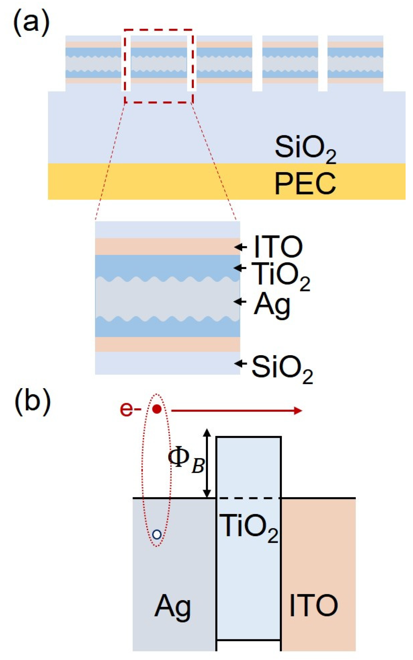
The plasmonic photodetector based on the TCO/Semiconductor/Metal configuration with grating is schematically shown in Figure 1a. The grating part of the top working area is composed of ITO/TiO2/Ag sandwich-like layers (red dotted box); where the outermost layer is covered with SiO2 as an anti-reflection layer to increase the absorption of incident light. The thicknesses of the ITO; TiO2; Ag; and anti-reflection layer are 20; 5; 25; and 268 nm; respectively. The period of the grating is 1030 nm and the Ag strip width is 950 nm. A perfectly matched layer (PEC) is used at the bottom as a light reflection layer to further enhance the interaction between the incident light and the metal grating; and the spacer layer is SiO2 with a thickness of 200 nm. Here, both sides of the metal layer are in contact with semiconductors; and hot electrons in the upper and lower directions can transfer to the metal/semiconductor interface; which increases the collection of hot electrons. It is emphasized that the roughened structure is introduced at the metal/semiconductor interface. As the hot electron reaches the interface and passes across the potential barrier (Figure 1b); momentum and energy conservation must be satisfied at the same time.
The deduction process of photogenerated hot electrons in a plasmonic photodetector can generally be divided into three processes: excitation, transport, and injection. When irradiated by incident light, the free electrons in the metal layer resonate and excite surface plasmons under the action of an external electric field, and then transfer the absorbed photon energy to electrons and excite them above the Fermi level. The photogenerated hot electrons can transfer to the metal/semiconductor interface without losing energy as the distance from the excitation position to the interface is shorter than the mean free path (MFP). If the hot electrons reaching the interface have sufficient energy and satisfy the condition of momentum conservation, they can overcome the potential barrier to pass across the metal/semiconductor interface, and then inject into the TCO electrode layer to form a photocurrent.
Therefore, the key to quantifying the transport process is to calculate the MFP, which is related to the energy of hot electron and can be expressed as [14]:
where the Bohr radius 𝑎0= 0.0529 nm, EF is the Fermi level, and 𝑟𝑠 is the radius of the sphere and equals to the volume of conduction electrons in Bohr radius. At low energy, is inversely proportional to the square of around 100 nm at 1.0 eV and 150 nm at 0.8 eV.
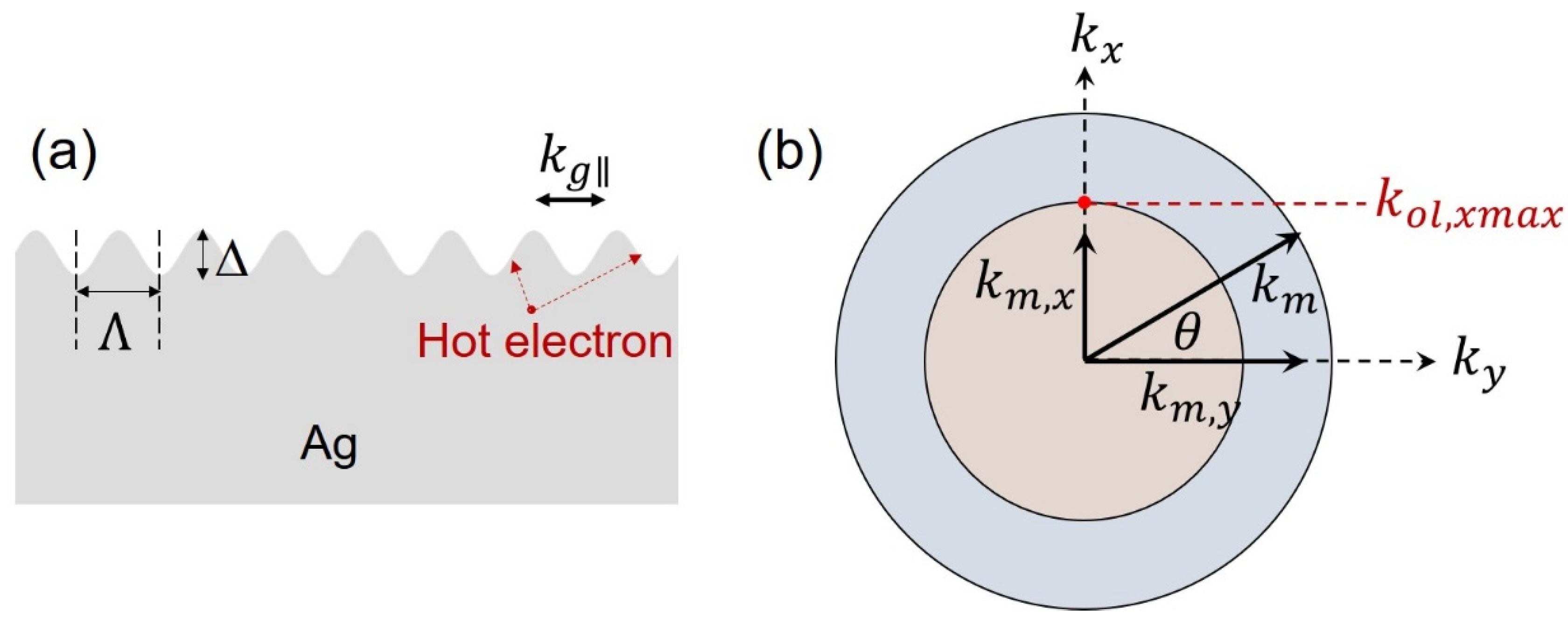
In order to clearly analyze the momentum characteristics of the hot electrons at the interface. Figure 2 provides the interrelationship of this process in momentum space. Here, the outer circle represents the momentum space of a hot electron on the metal side, and the inner circle represents the momentum space after the hot electron overcomes the potential barrier and enters the semiconductor side. When the hot electron passes across the interface, the wavevector is continuous in the direction parallel to the interface (), and the components in the metal and semiconductor sides along the direction perpendicular to the interface are denoted as and , respectively. It is seen that hot electrons can be injected into the semiconductor layer only when is satisfied. The energy of the photogenerated hot electron is (Eel: the kinetic energy of the hot electron above the Fermi level, ). The maximum escape angle θmax is obtained through Equation (6), where the electron is completely reflected if the angle between the moving direction of the hot electron and the normal direction the interface is greater than this angle θmax [5]:
Approximately, it is assumed that each incident photon excites a hot electron, and that the hot electron excitation energy is equal to the photon energy. The energy distribution of hot electrons after excitation is:
The probability that the photogenerated hot electrons transfer to the metal/semiconductor interface without losing energy is:
where d is the distance of the hot electron from the excitation site to the interface, and is the MFP in the metal.
While the injection process of hot electrons passes across the metal/semiconductor interface, the height of the potential barrier is related to the metal work function and the electron affinity of the semiconductor. Therefore, choosing different material systems can achieve photoresponse in different wavelengths. Here, the difference between the work function of Ag (4.26 eV) and the electron affinity of TiO2 (3.9 eV) is the height of 0.36 eV [16]. In this step of calculation, both the escape angle and the reflection of electrons at different materials are taken into account. In the communication band of 1550 nm, the maximum escape angle is quite small. According to the Equation (2), the calculated escape angle with smooth interface is . Obviously, only a small fraction of the hot electrons, which reach the interface and whose energies are higher than the potential barrier, can be injected across the potential barrier. Unfortunately, most of the hot electrons are scattered at the interface, and the energy would finally convert into Joule heat. This is one of the main reasons for the low photoresponsivity of plasmonic photodetectors in the infrared band [2,17,18,19]. With the blue shift of the wavelength, the escape angle become larger, so that the injection proportion of hot electrons increases. Owing to introducing a roughened interface, the extra momentum alleviates effectively the momentum mismatch the hot electrons on both sides of the interface.
When the orientation angle is within the maximum escape angle θmax, the transmittance (the ratio that can pass across the interface) can be calculated as:
where θi is the angle between the direction of motion and the normal direction of the interface when the hot electrons reach the interface; and TX is the transfer coefficient of M/S interface [20], .
In addition, the energy loss of the hot electrons can be ignored during the transport process in the semiconductor layer (oxide layer), because the MFP is much larger than the thickness of the oxide layer at 0.8 eV. The contribution of the very small fraction of the hot electrons with energies below the barrier through tunneling into the TCO layer is also negligible here.
The injection probability of the hot electron arriving and passing across the interface can be approximated as follows:
Based on the above analysis, finally, the external quantum efficiency (EQE) of the photodetector is calculated by the following formula:
where is the generation efficiency of hot electrons.
3. Results and Discussion
Here, the cosine curve is employed to simulate the roughness of the metal/semiconductor interface; therefore, the features of the roughened interface are described by the value of period Λ and cosine peak–valley height Δ. Meanwhile, in order to find the role of the roughened interface, the relative gain compared with the smooth interface device is calculated.
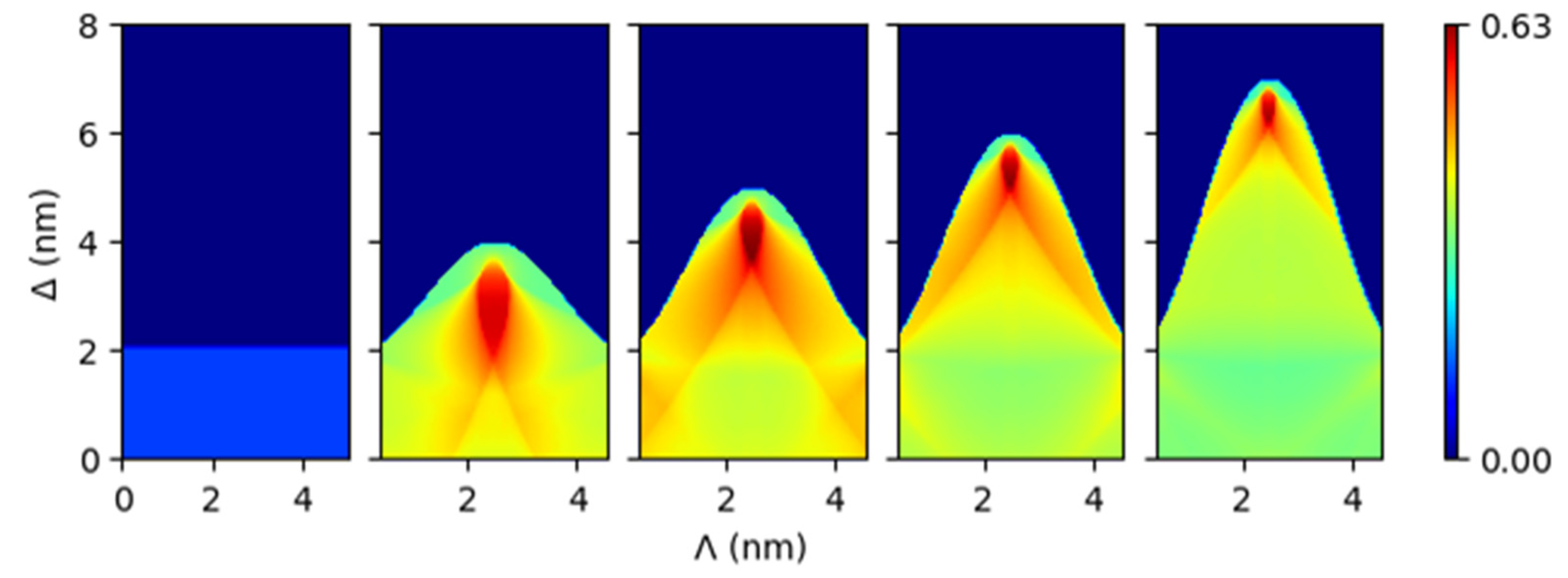
The injection probability of photogenerated hot electrons depends on the excitation site, motion direction, and kinetic energy during the process of the excitation-transport-injection. Manjavacas reported that the enhancement of hot electron injection probability in nano-elliptical spheroid particles, where both spheroid size and shape affect the efficiency [4]. With this interest in mind, similarly, the influence of the size and shape of the roughened interface on the injection efficiency of the plasmonic photodetectors is considered. The initial energy distribution of the electrons in the metal grating follows the free electron model [20,21]. The spatial distributions of the injection probability of the hot electrons excited at a certain position in the metal layer at Eel = 0.8 eV are provided in Figure 3. For a smooth interface device, the closer the excitation site of hot electron is to the interface, the less inelastic scattering is experienced, and the easier it is to collect. With a roughened interface, evidently, the highest conversion efficiency can reach 63% at Δ = 3 nm, and the injection probability is ~6 (estimated) times higher than that of a smooth interface device.
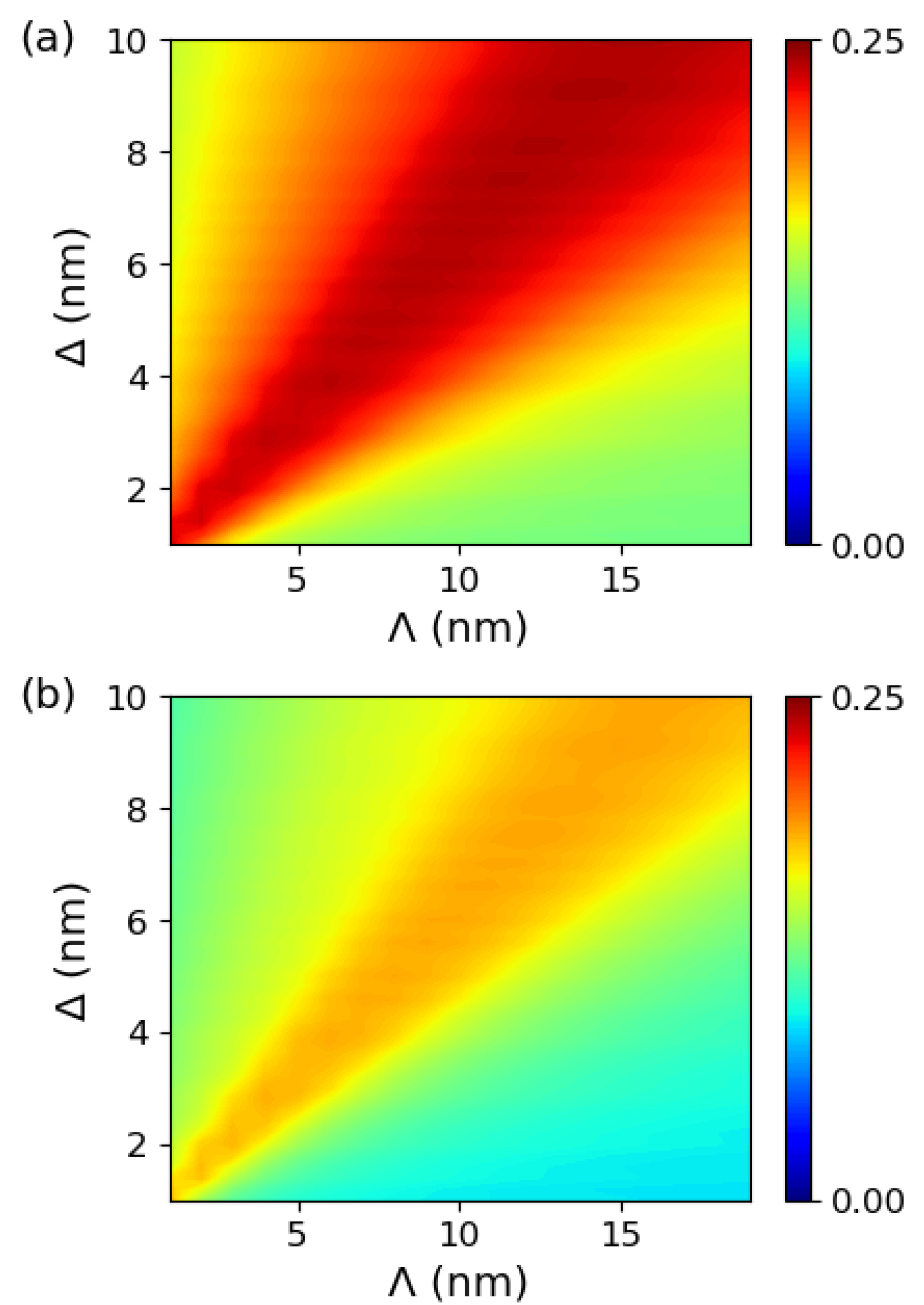
Furthermore, the excitation position of hot electrons in the metal grating is assumed to be uniform, the average injection probability in the entire metal grating is calculated relative to smooth interface device. As shown in Figure 4, the injection probability of hot electrons varies approximately twofold when the varies from 2 to 20 nm, and the Δ from 1 to 10 nm. Compared with the smooth interface device, the probability can be increased 7–8 times, breaking through the limitation brought by the maximum escape angle. It can be seen from Figure 4 that the average injection probability is optimal when the feature of the roughened interface is in the range of , which matches the theoretical prediction.
The simulation results show that there is a positive correlation between the incident photon energy and the injection efficiency of hot electrons. The height of the potential barrier decreases gradually. As the hot electron energy decreases, the escape angle become smaller and the injection efficiency reduces, as shown in Figure 5. The introduction of the roughened structure effectively reduces the interface reflection caused by the momentum mismatch. For hot electrons with low Eel (~0.5 eV), the relative gain can reach 8 times compared with the smooth interface device.
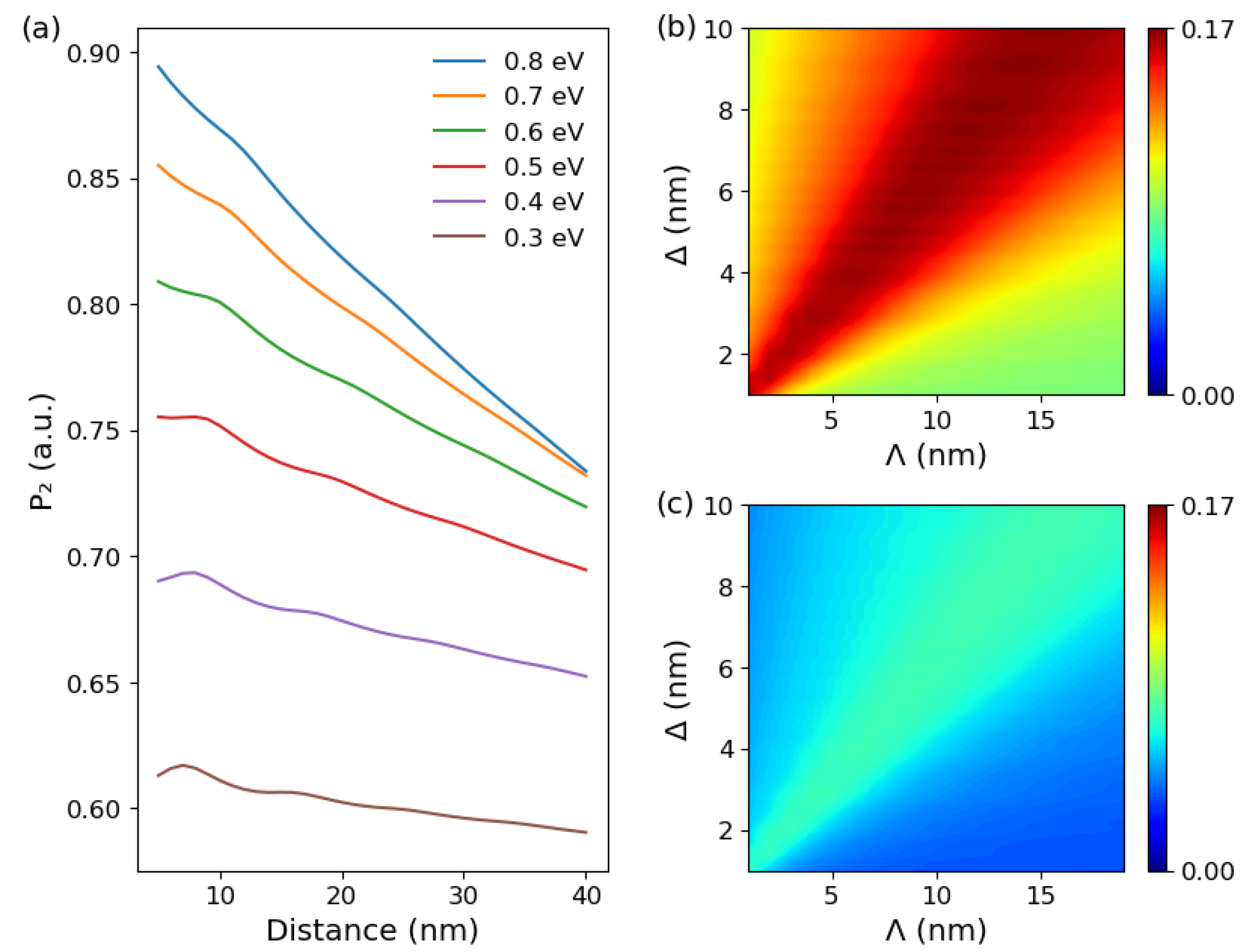
The higher the incident photon energy is, the higher the energy of the photogenerated hot electrons, and the greater the injection probability of passing across the potential barrier. As a result, the injection efficiency of hot electrons is also improved. Especially, in the case of the thickness of the grating being much smaller than the MFP, the roughness for moderating the momentum mismatch at the interface performs a more significant role in improving the quantum efficiency of the device. The injection efficiency of hot electrons as a function of distance to the top interface along the axis is shown in Figure 6a, which increases with closing to the interface, that is, with decreasing the thickness of the metal layer. For hot electrons with higher energies, the MFP is shorter, and the probability of inelastic scattering rises. Consequently, the attenuation of efficiency is greater than that of hot electrons with lower energies. In the case of the incident light with a single wavelength, the energy distribution of the photogenerated hot electrons can be described by the product of the densities of electronic states in initial and excited states. Figure 6b,c show the EQE of the photodetectors with various feature of roughened interface at incident light wavelengths 1550 and 2000 nm, respectively. The EQE at 2000 nm is only 50% of that at 1550 nm. The higher kinetic energy means that the proportion of hot electrons with energy higher than the M/S barrier increases, meanwhile the escape angle increases.
4. Conclusions
The plasmonic photodetectors based on the TCO/Semiconductor/Metal configuration with roughened interface were investigated numerically in order to improve photo responsivity. The simulated results using the FDTD method exhibit that the roughened structure effectively alleviates the momentum mismatch of hot electrons at the metal/semiconductor interface owing to asymmetry factor, thus breaking the limitation of the maximum escape angle and enhancing the injection efficiency of hot electrons. Moreover, it is noted that the injection efficiency is related to the features of roughened interface including the shape, period and height Δ. In the case of cosine curve model, the optimal value is in the range of . Combining with the double-sided injection structure, the hot electrons generated in almost all directions are well-utilized. The collection of hot electrons is further increased considering the fact that some hot electrons can be collected again after being reflected at another interface. Through optimized design of the device structure aiming at the incidence wavelength of 1550 nm, the injection efficiency of hot electrons is about 8 times higher than that of the smooth structure, which greatly increases photoresponsivity. Our work exhibits the approach and method to enhance the injection efficiency of hot electrons, which is of significance for the optimization of plasmonic photodetection devices.
Author Contributions
Conceptualization, L.X. and Y.S.; Methodology, L.X. and T.C.; Simulation, L.X.; Writing—Manuscript Preparation, L.X.; Writing—Review and Editing, S.Y., J.W. and Y.S. All authors have read and agreed to the published version of the manuscript.
Funding
This work was funded by the National Basic Research Program of China (Nos. 2018YFA0209100 and 2018YFA0307300), and the National Natural Science Foundation of China (Nos. 61991431, 61974064, 61921005 and 62005119), and the Excellent Youth Foundation of Jiangsu Scientific Committee (Grant BK20211538).
Institutional Review Board Statement
Not applicable.
Informed Consent Statement
Not applicable.
Conflicts of Interest
The authors declare no conflict of interest.
References
- Zhang, J.; Wang, Y.; Li, D.; Sun, Y.; Jiang, L. Engineering surface plasmons in metal/nonmetal structures for highly desirable plasmonic photodetectors. ACS Mater. Lett. 2022, 4, 343–355. [Google Scholar] [CrossRef]
- Hou, Y.; Liang, H.; Tang, A.; Du, X.; Mei, Z. Hot-electron photocurrent detection of near-infrared light based on ZnO. Appl. Phys. Lett. 2021, 118, 063501. [Google Scholar] [CrossRef]
- Xiao, H.B.; Lo, S.C.; Tai, Y.H.; Ho, Y.L.; Clark, J.K.; Wei, P.K.; Delaunay, J.J. Spectrally selective photodetection in the near-infrared with a gold grating-based hot electron structure. Appl. Phys. Lett. 2020, 116, 161103. [Google Scholar] [CrossRef]
- Manjavacas, A.; Liu, J.G.; Kulkarni, V.; Nordlander, P. Plasmon-induced hot carriers in metallic nanoparticles. ACS Nano 2014, 8, 7630–7638. [Google Scholar] [CrossRef] [PubMed]
- Chalabi, H.; Schoen, D.; Brongersma, M.L. Hot-electron photodetection with a plasmonic nanostripe antenna. Nano Lett. 2014, 14, 1374–1380. [Google Scholar] [CrossRef] [PubMed]
- Knight, M.W.; Sobhani, H.; Nordlander, P.; Halas, N.J. Photodetection with active optical antennas. Science 2011, 332, 702–704. [Google Scholar] [CrossRef]
- Jing, H.; He, J.; Peng, R.-W.; Wang, M. Aperiodic-order-induced multimode effects and their applications in optoelectronic devices. Symmetry 2019, 11, 1120. [Google Scholar] [CrossRef]
- Wen, L.; Chen, Y.F.; Liang, L.; Chen, Q. Hot-electron harvesting via photoelectric injection and photothermal heat relaxation in hotspots-enriched plasmonic/photonic disordered nanocomposites. ACS Photonics 2018, 5, 581–591. [Google Scholar] [CrossRef]
- Shen, L.; Poudel, N.; Gibson, G.N.; Hou, B.Y.; Chen, J.H.; Shi, H.T.; Guignon, E.; Page, W.D.; Pilar, A.; Cronin, S.B. Plasmon resonant amplification of a hot electron-driven photodiode. Nano Res. 2018, 11, 2310–2314. [Google Scholar] [CrossRef]
- Fang, Y.R.; Jiao, Y.; Xiong, K.L.; Ogier, R.; Yang, Z.J.; Gao, S.W.; Dahlin, A.B.; Kall, M. Plasmon enhanced internal photoemission in antenna-spacer-mirror based Au/TiO2 nanostructures. Nano Lett. 2015, 15, 4059–4065. [Google Scholar] [CrossRef]
- Dong, X.Y.; Zheng, D.Y.; Lu, J.; Niu, Y.R.; Liu, B.B.; Wang, H. Plasmon-enhanced lateral photovoltaic effect observed in Ag-ZnO core-shell nanoparticles. Appl. Phys. Appl. Phys. Lett. 2021, 118, 122101. [Google Scholar] [CrossRef]
- Gong, T.; Munday, J.N. Angle-Independent Hot carrier generation and collection using transparent conducting oxides. Nano Lett. 2014, 15, 147–152. [Google Scholar] [CrossRef] [PubMed]
- Sobhani, A.; Knight, M.W.; Wang, Y.M.; Zheng, B.; King, N.S.; Brown, L.V.; Fang, Z.Y.; Nordlander, P.; Halas, N.J. Narrowband photodetection in the near-infrared with a plasmon-induced hot electron device. Nat. Commun. 2013, 4, 1643. [Google Scholar] [CrossRef] [PubMed]
- Leenheer, A.J.; Narang, P.; Lewis, N.S.; Atwater, H.A. Solar energy conversion via hot electron internal photoemission in metallic nanostructures: Efficiency estimates. J. Appl. Phys. 2014, 115, 134301. [Google Scholar] [CrossRef]
- Grajower, M.; Levy, U.; Khurgin, J.B. The role of surface roughness in plasmonic-assisted internal photoemission schottky photodetectors. ACS Photonics 2018, 5, 4030–4036. [Google Scholar] [CrossRef]
- Wu, K.; Zhan, Y.H.; Wu, S.L.; Deng, J.J.; Li, X.F. Surface-plasmon enhanced photodetection at communication band based on hot electrons. J. Appl. Phys. 2015, 118, 063101. [Google Scholar] [CrossRef]
- Zhou, D.M.; Li, X.F.; Zhou, Q.H.; Zhu, H.M. Infrared driven hot electron generation and transfer from non-noble metal plasmonic nanocrystals. Nat. Commun. 2020, 11, 2944. [Google Scholar] [CrossRef]
- Khurgin, J.B. Fundamental limits of hot carrier injection from metal in nanoplasmonics. Nanophotonics 2020, 9, 453–471. [Google Scholar] [CrossRef]
- Christopher, P.; Moskovits, M. Hot charge carrier transmission from plasmonic nanostructures. Annu. Rev. Phys. Chem. 2017, 68, 379–398. [Google Scholar] [CrossRef]
- Ng, C.; Cadusch, J.J.; Dligatch, S.; Roberts, A.; Davis, T.J.; Mulvaney, P.; Gómez, D.E. Hot carrier extraction with plasmonic broadband absorbers. ACS Nano 2016, 10, 4704–4711. [Google Scholar] [CrossRef]
- Li, W.; Valentine, J. Metamaterial perfect absorber based hot electron photodetection. Nano Lett. 2014, 14, 3510–3514. [Google Scholar] [CrossRef] [PubMed]
Figure 1.
(a) Schematic diagram of the device structure. The red dotted box is the effective hot electron collection area. (b) Schematic diagram of the energy band.
Figure 1.
(a) Schematic diagram of the device structure. The red dotted box is the effective hot electron collection area. (b) Schematic diagram of the energy band.

Figure 2.
(a) Surface parameters of a grating. (b) Momentum space of a hot electron, in the metal (outer), the semiconductor layer (inner).
Figure 2.
(a) Surface parameters of a grating. (b) Momentum space of a hot electron, in the metal (outer), the semiconductor layer (inner).

Figure 3.
Spatial distribution of injection probability with different heights of roughened interface. Eel = 0.8 eV, from left to right as smooth, roughened interface, period = 5 nm, height Δ from 2 to 5 nm.
Figure 3.
Spatial distribution of injection probability with different heights of roughened interface. Eel = 0.8 eV, from left to right as smooth, roughened interface, period = 5 nm, height Δ from 2 to 5 nm.

Figure 4.
Distribution of average injection probability with different periods and heights of roughened interface at the energies: (a) Eel = 0.8 eV, (b) Eel = 0.4 eV.
Figure 4.
Distribution of average injection probability with different periods and heights of roughened interface at the energies: (a) Eel = 0.8 eV, (b) Eel = 0.4 eV.

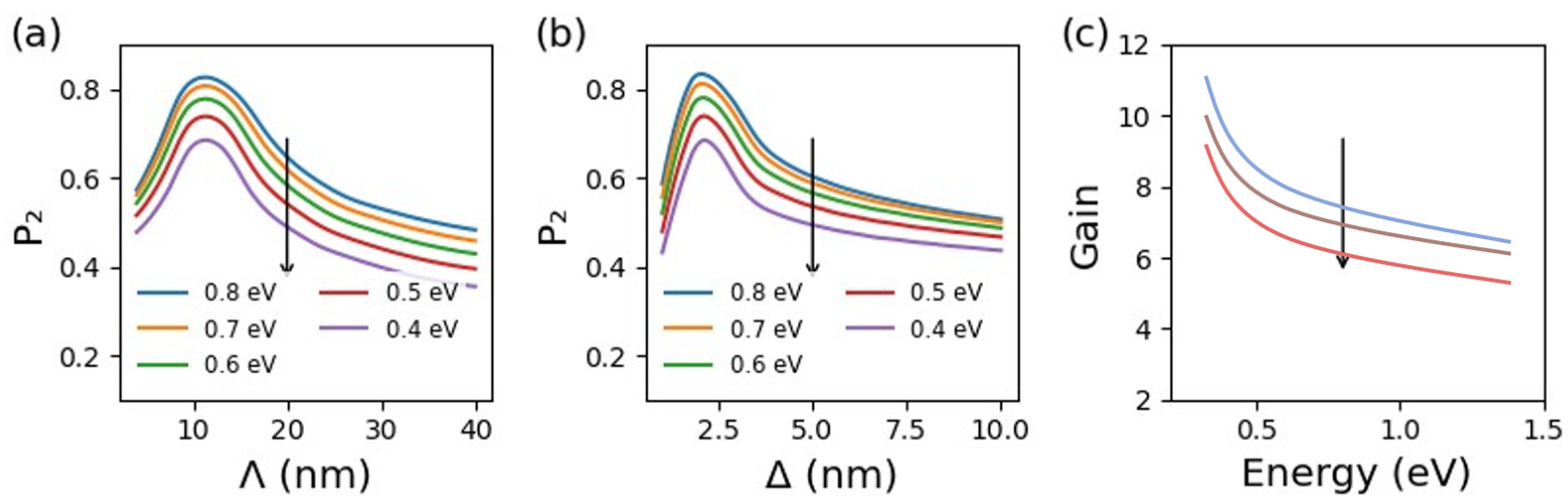
Figure 5.
Maximum value of the injection probability as a function of the period and height at different Eel from 0.4 to 0.8 eV: (a) Δ = 6 nm. (b) Λ= 5 nm. (c). Relative gain as the function of Eel at different Δ = 4, 6, and 8 nm (from top to bottom), and Λ = 10 nm.
Figure 5.
Maximum value of the injection probability as a function of the period and height at different Eel from 0.4 to 0.8 eV: (a) Δ = 6 nm. (b) Λ= 5 nm. (c). Relative gain as the function of Eel at different Δ = 4, 6, and 8 nm (from top to bottom), and Λ = 10 nm.

Figure 6.
(a) Injection probability as a function of distance to the top interface along the axis (b), and (c) distribution of EQE with different periods and heights of roughened interface at incident light wavelengths 1550 and 2000 nm, respectively.
Figure 6.
(a) Injection probability as a function of distance to the top interface along the axis (b), and (c) distribution of EQE with different periods and heights of roughened interface at incident light wavelengths 1550 and 2000 nm, respectively.

Publisher’s Note: MDPI stays neutral with regard to jurisdictional claims in published maps and institutional affiliations. |
© 2022 by the authors. Licensee MDPI, Basel, Switzerland. This article is an open access article distributed under the terms and conditions of the Creative Commons Attribution (CC BY) license (https://creativecommons.org/licenses/by/4.0/).
Share and Cite
MDPI and ACS Style
Xiao, L.; Yan, S.; Chen, T.; Wang, J.; Shi, Y. Enhancing Hot Electron Injection in Plasmonic Photodetectors through Roughened Interfaces. Symmetry 2022, 14, 1628. https://0-doi-org.brum.beds.ac.uk/10.3390/sym14081628
AMA Style
Xiao L, Yan S, Chen T, Wang J, Shi Y. Enhancing Hot Electron Injection in Plasmonic Photodetectors through Roughened Interfaces. Symmetry. 2022; 14(8):1628. https://0-doi-org.brum.beds.ac.uk/10.3390/sym14081628
Chicago/Turabian StyleXiao, Long, Shancheng Yan, Tianhong Chen, Junzhuan Wang, and Yi Shi. 2022. "Enhancing Hot Electron Injection in Plasmonic Photodetectors through Roughened Interfaces" Symmetry 14, no. 8: 1628. https://0-doi-org.brum.beds.ac.uk/10.3390/sym14081628
Note that from the first issue of 2016, this journal uses article numbers instead of page numbers. See further details here.