

Temperature-Dependent Phase Variations in Van Der Waals CdPS3 Revealed by Raman Spectroscopy


1
Department of Materials Science and Engineering, Monash University, Melbourne 3800, Australia
2
ARC Centre of Excellence in Exciton Science, Monash University, Melbourne 3800, Australia
3
School of Engineering, College of Engineering and Computer Science, The Australian National University, Canberra 2601, Australia
4
Centre for Quantum Computation and Communication Technology, School of Engineering, Australian National University, Canberra 2601, Australia
*
Authors to whom correspondence should be addressed.
Symmetry 2024, 16(2), 140; https://0-doi-org.brum.beds.ac.uk/10.3390/sym16020140
Submission received: 7 December 2023
/
Revised: 18 January 2024
/
Accepted: 19 January 2024
/
Published: 24 January 2024
(This article belongs to the Special Issue Symmetry/Asymmetry in 2D Materials)
Abstract
:In addition to graphene, the transition metal dichalcogenides, black phosphorus and multiple other layered materials have undergone immense investigations. Among them, metal thiophosphates (MPSx) have emerged as a promising material for various applications. While several layered metal thiophosphates with general-formula MPSx have been scrutinized extensively, van der Waals (vdW) CdPS3 has been overlooked in the literature. Here we report on the extensive Raman scattering of layered CdPS3, showing structural phase transition at a low temperature. The emergence of multiple new peaks at low frequency and a significant shift in peak position with temperature implied a probable change in crystal symmetry from trigonal D3d to triclinic Ci below the phase transition temperature, TK~180 K. In addition, we also showed a p-type performance of CdPS3 FET fabricated using Au electrodes. This work adds CdPS3 to the list of potential layered materials for energy application.
1. Introduction
The discovery of intrinsic van der Waals two-dimensional (2D) material has attracted immense interest from the material science and nanomaterials community [1,2,3,4,5]. Extensive investigations have been carried out on the electrical, optical, mechanical and chemical properties of layered materials, which have witnessed applications in multidisciplinary fields [2,6,7,8]. In addition to numerous optoelectronic devices [9,10], like transistors, diode, LEDs, photovoltaics and solar cells, layered materials have also been applied to catalytic activity for future roles in energy alternatives, (bio)sensing systems and advanced electronic devices [11,12,13,14]. With the advent of new synthesis techniques and emergence of various materials in the vdW 2D family, attention has recently been turned to other 2D materials besides graphene [15,16,17], transition metal dichalcogenides (TMDs) [18,19,20] and black phosphorus [12,21]. The search for enhanced electrical, optical and magnetic properties has led to the manifestation and synthesis of metal phosphorus chalcogenides with a general formula of MPXY [22].
The family of MPXY has a layered structure possessing the van der Waals gap. M represents the transition metal (TM) atom (e.g., Mn, Fe. Co, Ni and Cd), X is a chalcogenide atom (either S or Se) and Y is the number of chalcogen atoms [23]. Several studies have reported on the alluring electronic, anisotropic, magnetic, dielectric, structural and optical properties of these materials, which can be easily exfoliated down to monolayer thickness [22,24,25,26,27]. This is because they are held together by weak van der Waals forces, similar to other layered compounds, and can be thinned down to fewer sheets [28]. Their structures are also similar where the metal and phosphorus atoms within each layer are sandwiched in between the chalcogenide atoms [23]. MPXY compounds have vital intrinsic properties that are useful in multifarious processes. Their layered structures have manifested anisotropic properties, giving them the ability to act as host lattices for intercalation compounds [29]. MPXY compounds also tend to possess unusual intercalation–reduction behavior, in addition to incipient ionic conductivity, influencing their usage in Li-ion batteries [30,31], gas storage [32] and various other photo-electrochemical reactions [33]. They also tend to have a wide range of band gaps that suggest possible optoelectronic applications in a broad wavelength range.
According to computational results and experimental verification, MPXY compounds are the most popular functional materials because of their intermediate bandgaps from 1.3 to 3.5 eV, implying their enhanced light absorption compared to transition metal dichalcogenides (TMDs) [34,35]. Most interestingly, magnetic moments have been found to be localized in the transition metal ions that form a honeycomb network structure, giving rise to antiferromagnetism (AFM) beyond a certain transition or Neel temperature, TK [36]. For instance, MnPS3 shows AFM beyond 78 K, while FePS3 and NiPS3 show AFM beyond 116 K and 155 K, respectively [37,38,39]. However, these were only manifested when the transition atom was magnetic [40]. Furthermore, it has been demonstrated that the magnetic properties can also be tuned via alloying with nonmagnetic transition metals [41]. Raman scattering has been promoted as the pivotal and significant tool to study such phase transitions in these materials, where clear signatures of phase transition emerges beyond TK in form of new phonon peaks or a large positional shift in the existing phonon modes [38,39,42,43].
While a majority of the members in the MPXY family have been shown to have AFM and have been studied extensively, some essential compounds, especially the nonmagnetic ones, have been mostly overlooked in the literature. CdPS3, for example, is a diamagnetic compound due to its core electrons, but it does not manifest AFM due to the Cd ion being nonmagnetic [44]. It generally belongs to the C2/m space group with monoclinic symmetry, which results from a small distortion in the rhombohedral structure (trigonal space group R3(C23i)) but can take other phases or symmetry at room temperature when synthesized in various forms. Earlier investigation by Lifshitz et al. [45], using electron paramagnetic resonance (EPR) and X-ray diffraction on Mn-doped CdPS3 crystals, revealed a phase transition from monoclinic to orthorhombic, around 260 K. With the decreasing temperature, they found that the crystal symmetry became higher, and there was a loss of unique axis corresponding to the monoclinic phase.
Some researchers have explored the phase change in the CdPS3 compound from C2/m to R3 through the introduction of external pressure and analyzing pressure-dependent Raman spectra [46]. Others have investigated the interlayer coupling in a CdPS3 nanosheet-based membrane through conductivity and transport measurements [47]. Computational and theoretical efforts have also been instigated with an aim to view the molecular structure and bond vibrations [48]; however, it was not substantiated through intensive experimental analysis. Regardless, there is no comprehensive reporting on the nonlinear optical properties of layered CdPS3, despite its being an important compound for future applications in energy storage devices and the development of biosensing system [44]. It is essential to completely understand the vibrational properties, phase segregation and lattice dynamics incurred by the thermal effects on this material, as they can have vital implications for future device fabrication and advanced manufacturing using CdPS3. Low-frequency Raman spectroscopy provides an intriguing non-evasive technique to probe such properties and comprehend the phase structure of this material. The aim of this study mostly involves providing a detailed analytical investigation on the low- and high-frequency vibrational dynamics of CdPS3 and phase segregation with temperature. In this work, we used high-resolution Raman spectroscopy to characterize bulk CdPS3 to uphold its precise phase transition from trigonal to monoclinic. The thermal dependence of the Raman spectrum clearly indicates a phase transition temperature of TK~178–180 K. We analyzed the peak position and vibrational intensity of several Raman modes that correlate well with symmetric change to monoclinic phase. Furthermore, we also fabricated a field effect transistor (FET) by using thin layers of CdPS3, which showed a p-type response and good hole mobility, allowing its application in major electronic devices.
2. Results and Discussions
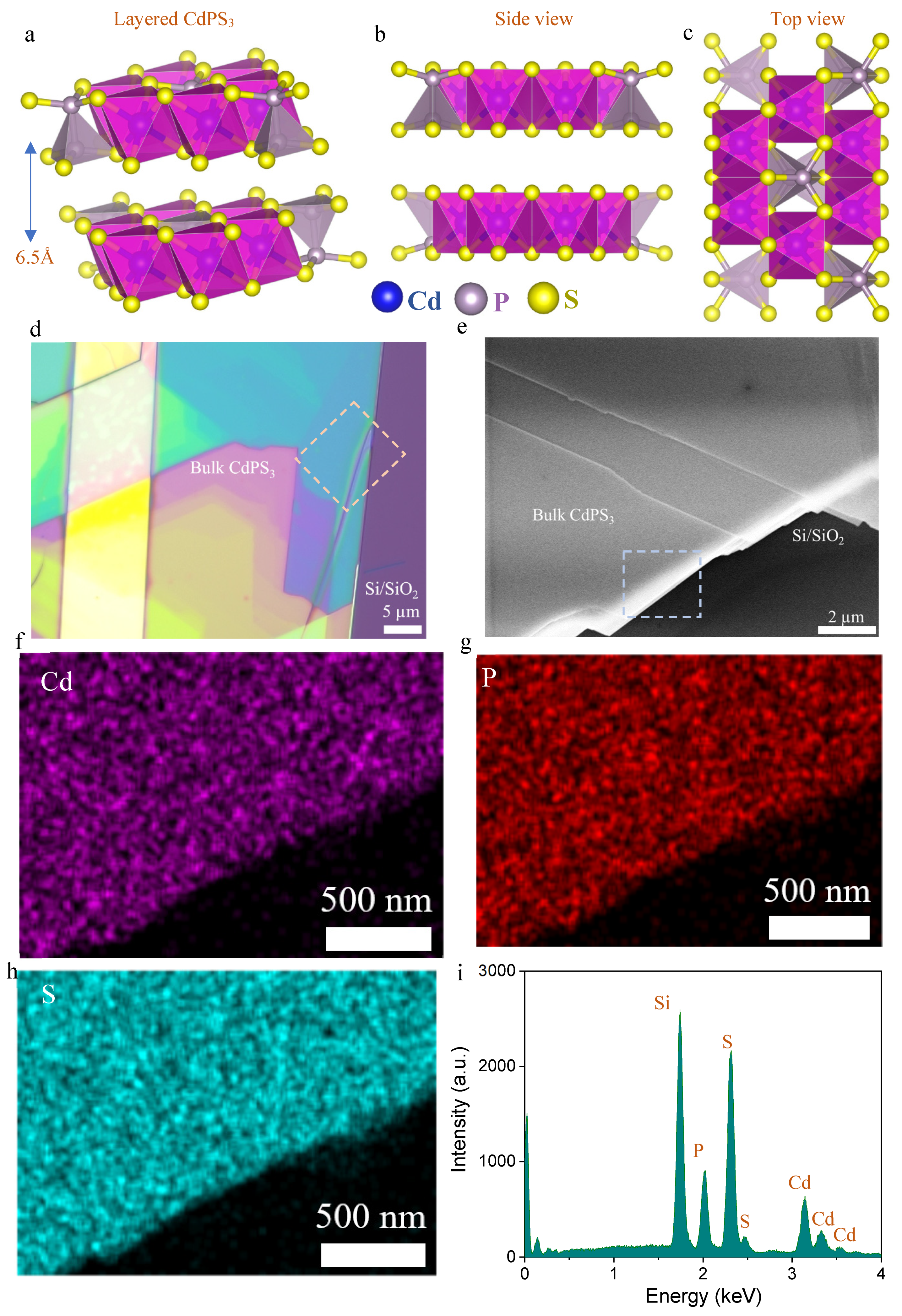
CdPS3 belongs to a family of quasi two-dimensional materials. Figure 1a shows the schematic representation of the crystal structure, and Figure 1b,c show the top view and side of the crystal. It is isostructural, with the transition metal atom, Cd, forming a honeycomb lattice in planes that are weakly bound by van der Waals forces [P2S6]4−. An anion sublattice appears within each layer, and the honeycomb arrangement of the transition metal ion is distributed around the [P2S6]4− bipyramids such that TM atom is surrounded by six sulfur atoms. These sulfur atoms are further connected to two phosphorus atoms above and below the TM plane. Single crystals of CdPS3 were sourced commercially (2D semiconductors) and exfoliated mechanically (see Section 4). The samples were then transferred to Si/SiO2 substrate for further optical characterization. Figure 1d shows a typical CdPS3 bulk sample on a SiO2 substrate, exfoliated mechanically and transferred using the vdW transfer technique (see Methods section). At first, we confirmed the sample stoichiometry by using scanning electron microscope (SEM) and energy-dispersive X-ray spectroscopy (EDX). Figure 1e shows the SEM image of a section of the bulk sample in Figure 1d, showing a relatively smooth surface. The corresponding energy-dispersive spectrometry (EDS) spectrum is shown in Figure 1f–h, highlighting the uniform elemental composition of Cd, P and S in the layered material. The Cd-L line and K line of P and S can be easily excited using 5 kV excitation energy during SEM and EDS measurements. Figure 1i shows the EDS spectrum, indicating the peak energies of each of the constituent elements. Hence, within the limitation of the technique, the samples examined in this work does not exhibit detectable unwanted impurities.
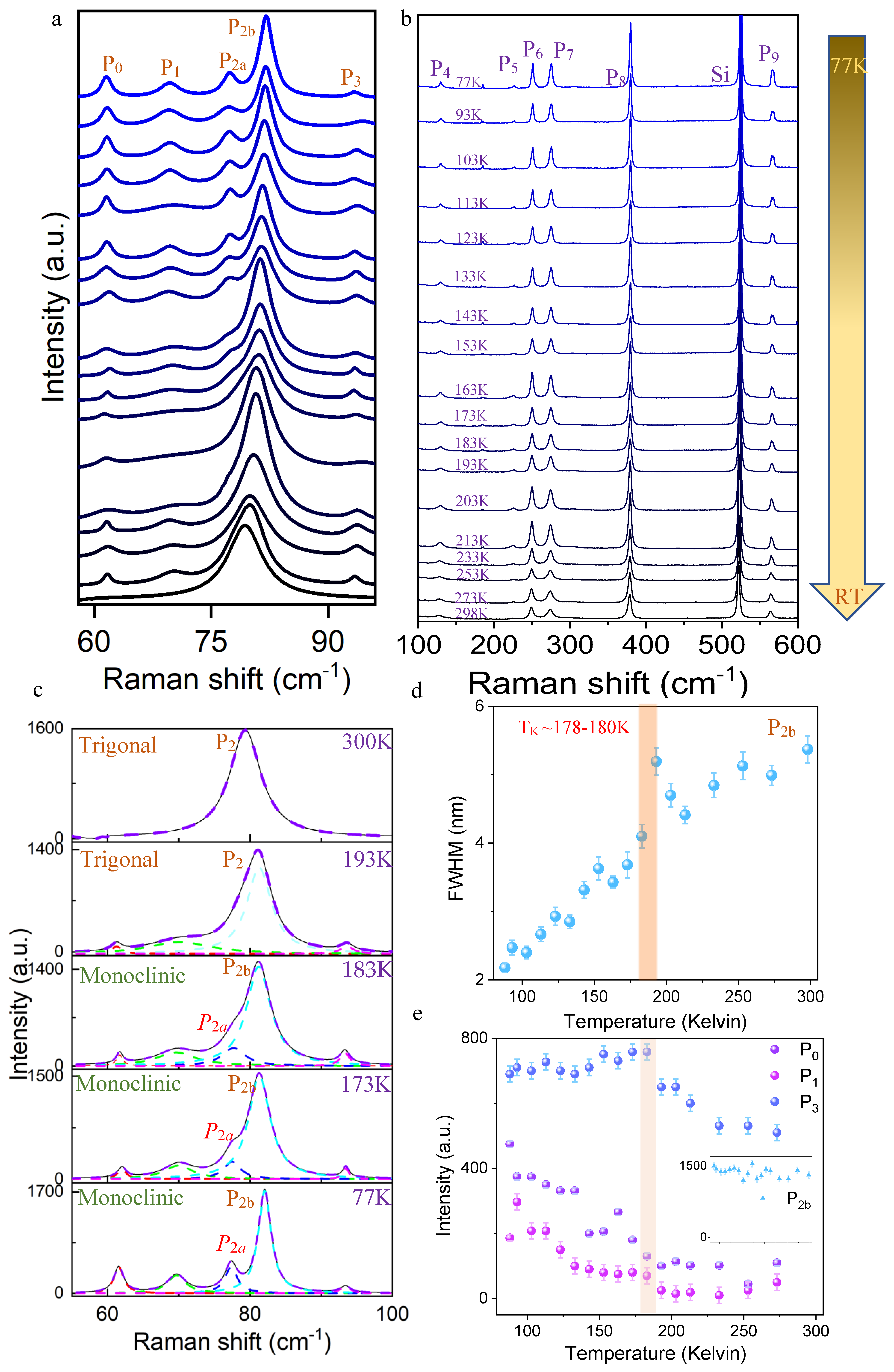
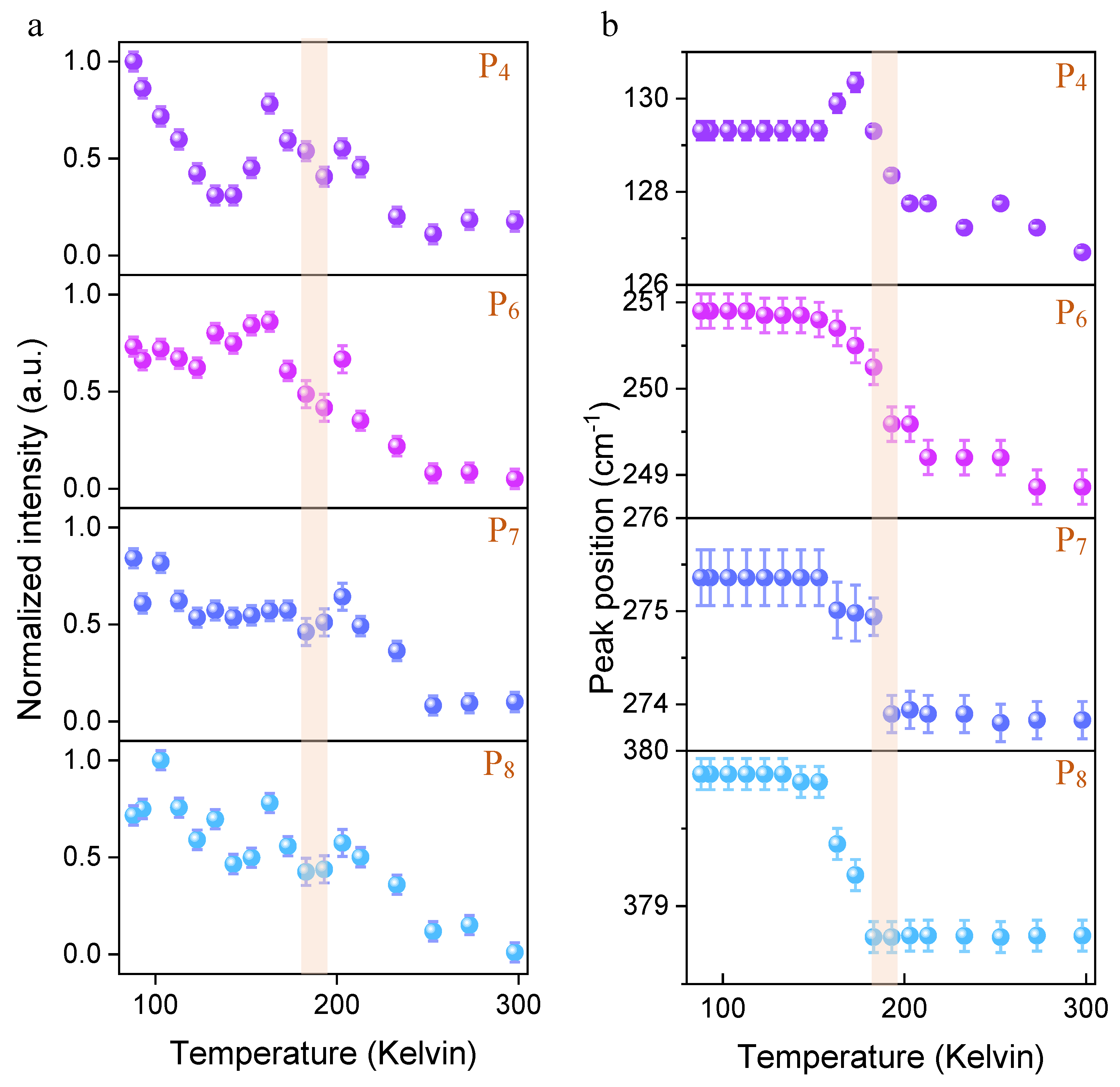
Raman measurements were consequently carried out on bulk CdPS3 samples, using a commercial micro-Raman system. Figure 2a,b show the temperature dependence of Raman spectra from 55 to 95 cm−1 and from 100 to 600 cm−1, respectively, from RT down to 77 K. As witnessed, multiple peaks can be identified both at RT and 77 K. In the low-frequency regime, only the P2 peak is recorded around 79.9 cm−1 at RT. With a decreasing temperature, more new phonon modes start to appear, marked by P0, P1, P2a, P2b and P3. This signifies that the material is undergoing substantial changes as the temperature is lowered. In the high-frequency regime, peaks P4, P5, P6, P7, P8 and P9 can be detected from RT, but the visual examination manifests a clear change in the peak position and vibrational intensity. Such a change in mode position and intensity can also be observed for low-frequency peaks. To clearly emancipate the transition temperature, TK, we carried out Lorentzian fitting of the experimental curves to disintegrate and analyze each peak separately. Figure 2c shows some representative Raman spectra with fitting curves, with particular focus around TK. Peak 2 splits into P2a and P2b at around ~178–180 K, manifested meticulously by Lorentzian fitting curves, implying a clear phase transition. Figure 2d shows the full width at half maximum (FWHM) of peak P2b, which decreases progressively with the temperature, but around TK, it shows a sudden augmentation before decreasing again. Figure 2e shows the normalized intensity of peaks P0, P1 and P3 in the low-frequency regime, which suddenly increases in strength around 178–180 K. This clearly signifies that the material is undergoing a phase transition around that temperature. This is in slight contradiction with the previously reported value of 228 K for CdPS3 single crystals deduced from X-ray diffraction [49]. Figure 3 shows the summary of peak position and intensity of other high-frequency Raman modes, thus further reaffirming the phase transition of CdPS3. The peak intensity of P4, P6, P7 and P8 increases gradually with the decrease in temperature; around TK, it shows sudden nonuniformity. Similarly, the peak position of the higher Raman modes shows a sudden blue shift around TK, and then the modes become insensitive with temperature.
Such an observation in Raman spectra can be correlated with the phase transition of CdPS3 from trigonal at a high temperature to monoclinic at a low temperature. The phonon mode P2a appears only at the low temperature and vanishes above ~180 K. This soft mode is strongly related to the structural phase transition. Liftshitz et al. [45] observed a hysteresis loop in CdPS3 single crystals at a higher temperature and suggested the co-existence of multiple phases before the first order phase transition occurs. However, we observed that the P2a mode disappears completely above ~180 K; in principle, first-order phase transition should not nullify the frequency of the mode at the transition temperature [50]. Hence, this indicates that the phase transition is more of a displacive type. Generally, it is plausible to observe more Raman peaks in the low symmetric phase than in the high symmetric phase. The appearance of new mode P2a and the increase in intensity of other low-frequency Raman modes, like P0, P1 and P3, suggest that the crystal symmetry decrements with the reduction in temperature through the phase transition.
The high-temperature phase of CdPS3 consists of degenerate phonon modes, as denoted by the two- or three-dimensional representation, because the peak P2 splits into two peaks at a low temperature [50]. Since CdPS3 has a layered structure, peak P2 can be assigned to the doubly degenerate Raman active mode in the high-temperature phase. Splitting into two peaks can be denoted as one-dimensional representations in the low-temperature phase. Hence, the symmetry of the crystal should be reduced at a low temperature. Lifshitz et al. [45] claimed, in an earlier investigation, that the high-temperature phase would be monoclinic; however, there are no degenerate modes that can be denoted by the two- or three-dimensional representations, thus contradicting their conclusion.
Alternately, our observation can be explained well considering the fact that the high-symmetry phase belongs to trigonal symmetry, as claimed by Covino et al. in an earlier report [51]. All MPXy crystals have a layered structure due to the weakly interacting van der Waals interaction, and the symmetry of a single layer belongs to the trigonal symmetry D3d in almost all members of MPXy family. Also, two formula units are present in the primitive unit cells. Assuming that the crystal symmetry of CdPS3 belongs to trigonal symmetry, D3d, the phonon modes at Γ can be decomposed into the following representations [50,52]:
Γ = 3A1g + 2A2g + 5Eg + A1u + 4A2u + 5Eu
A1g and Eg modes are Raman active among these, and their Raman tensors can be denoted as follows:
One A2u mode and Eu mode can be considered to be acoustic modes, while A2u and four Eu modes are infrared active. Hence, they cannot be detected in the Raman spectra extracted using a green laser. Therefore, at RT, the high-frequency Raman active modes can be assigned to the vibration of P2S6 units with D3d symmetry [44]. Modes P6 and P8 at ~248 cm−1 and ~378 cm−1, respectively, can be assigned to A1g; meanwhile, modes P4, P5, P7 and P9 at 126.5 cm−1, 224.8 cm−1, 273.42 cm−1 and 563.30 cm−1, respectively, can assigned to Eg [44]. Such phonon modes originating from the symmetry of P2S6 units are also common in compounds of the MPS3 family [53]. Infrared spectroscopic analyses of CdPS3 single crystals on the basal layer planes were carried out by Mathey et al. [54]; they observed three strong absorption bands at 193 cm−1, 252 cm−1 and 564 cm−1, and they also noted another band at around 110 cm−1 with dual peaks that was regarded as a superposition of a strong and weak peak. These were assigned to Eu modes that are only detectable under infrared excitation. Furthermore, Mathey et al. observed some Raman modes at 310 and 449 cm−1 that correlated with Au modes. Hence, these signatures were absent in our Raman study. Therefore, based on the current analysis, it is reasonable to expect that the high-temperature phase of CdPS3 is D3d and belongs to trigonal symmetry (R3). Peak P2 can be assigned to the Eg mode in the trigonal symmetry, which was split into two peaks in the low-temperature phase. If we assume that the Landau theory is applicable to the present phase transition of CdPS3, then it can be regarded as a weakly first-order variation. Hence, it is plausible to assume that the crystal point group of the low-temperature phase is one of the subgroups of the high-temperature phase. Considering the appearance of new Raman modes, enhancement of vibrational intensity and significant blue shift of the phonon modes, it can be suggested that crystal symmetry changes from the trigonal symmetry, D3d, to triclinic symmetry, Ci. This transition occurs at around TK = ~178–180 K. Tomoyuki Sekine et al. [50] observed some similar transition on CdPS3 single crystals and mentioned the possibility of other monoclinic-symmetry C2h, C2 and Cs at a low temperature. However, we also observed peaks P0, P1 and P3 at a low temperature, which has not been reported before. It is reasonable to assume that the low-temperature phase forms a complex phase structure consisting of one of the monoclinic symmetries (C2/m). This can make some Raman modes active at 61.37 cm−1, 70 cm−1 and 93.3 cm−1. As deduced before, high-frequency phonon modes originate from the internal vibrations of P2S6 octahedrons, while the low-frequency Raman modes are mostly due to the vibrations of the transition metal ion, Cd. Hence, the structural phase transition occurs as a result of the displacement of the Cd ion. This can be related to the observation of new peaks (P0, P1 and P3) and the increase in their intensity below the transition temperature.
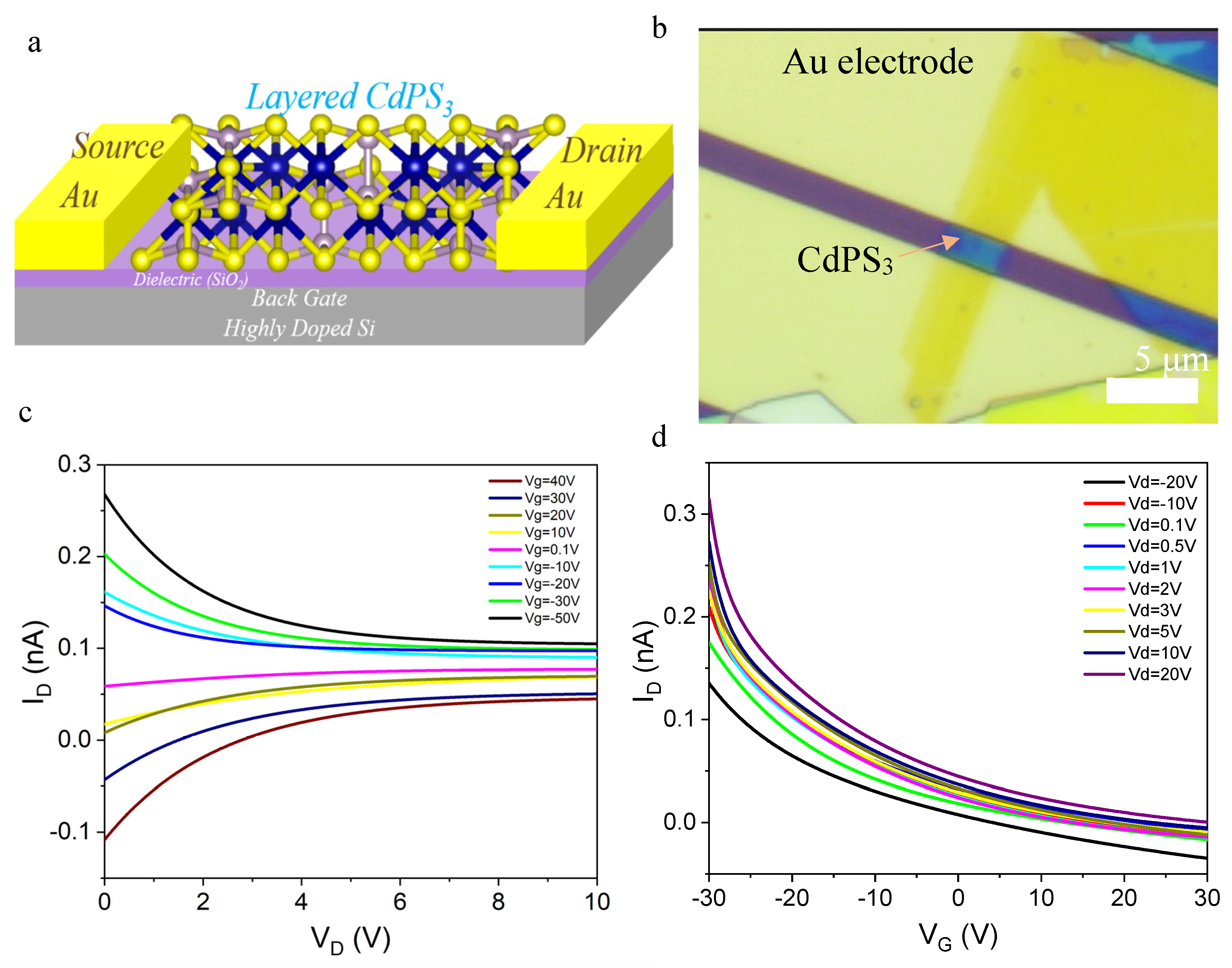
Finally, we fabricated the field effect transistor (FET) from the vdW-layered CdPS3. The schematic structure of back-gated FET is shown in Figure 4a. SiO2 was used as the dielectric, and Au contacts were used as the source and drain terminals. Highly doped Si provides a good source for back-gate voltage. To fabricate the FET structure, conventional optical lithography was deployed to pattern the Au electrodes on the Si/SiO2 substrate. The process involved UV exposure after spin-coating with photoresist metal evaporation, using e-beam evaporation and, finally, lift-off to obtain the patterns. The 2D material was then transferred mechanically using the vdW transfer technique, such that the source and drain electrodes were in contact with the sample. An optical image of a typical FET is shown in Figure 4b. The channel length is 2 µm, and a large-sized bulk sample is present in between the channels. The output characteristics of the device, source-drain current (Ids) as a function of source-drain voltage (Vds) and transfer characteristic, drain current as function of back gate (Vg) is shown in Figure 4c,d. All electrical properties of CdPS3 back gated FET were measured at room temperature in air. The current increases with increasing negative back gate voltage, suggesting p-type behaviors [55]. P-type semiconductors are indispensable in many complex digital electronics, such as inverters, logic gates, memory devices and integrated circuits (ICs) [56]. The nonlinear behavior may arise from the Schottky barrier contact with Au metal [57]. The field effect mobility can be extracted from the Ids-Vg curve, using the following expression:
where µ is the mobility, W (2 µm) is the channel width, L is the channel length and Ci (1.418 × 10⁻⁴ F.m−1) is the capacitance between the channel and back gate per unit area (; ε0 = 8.85 × 10⁻¹² F.m−1; εr = 3.9; d = 275 nm). The mobility value can be determined to be 0.1–0.5 cm2/Vs. The low mobility compared to several other devices in the literature could be due to the poor contact with metal electrode, as reported earlier in case of WSe2 and MoS2 [55]. It may also be possible to improve the performance by using high-K dielectric materials in top-gated devices [58,59,60].
Two-dimensional p-type semiconductors provide extensive advantages and benefits for designing CMOS inverters with unique and desirable properties. Such CMOS designs with p-type FET allow for a simple electrode structure (Vin) and circuit planning that result in an elevated gain and lower operating voltage (Vdd). P-type 2D semiconductors can also provide a solid support for developing new junction inverters with lower power consumption, which is vital for future consumer electronics. With the development of the p-type 2D semiconductor, CMOS logic circuits based on p-type FET present multifarious advantages in terms of computational densities and reconfigurable capabilities of single devices [56]. They also offer key advantages due to their ability to operate with positive voltage in regard to the source terminal, which simplifies the integration process of these components in circuits where a positive power supply is essential. This also makes p-type FET well suited in power electronics, like load switching and battery management. In addition, the negligible ON-state resistance of P-channel FETs suppresses power losses and contributes to enhanced energy efficiency, making them a favorable candidate for battery-operated devices and energy-conscious systems.
The development of digital electronics has manifested specific requirements in terms of channel length, switching characteristic and contact resistivity, eventually integrating them into modern Si-dominant electronics. Recent studies have also indicated that p-type 2D semiconductors exhibit great application potential in logic device design, although their performance is yet to reach the theoretical bottleneck. Fortunately, the p-type 2D semiconductors with atomic thickness and surfaces with dangling bonds are promising channel candidates, and CdPS3 provides a unique leverage in the family of transition metal thiophosphates. Although mobility is not at the ideal mark, multiple device improvements, like reducing the Schottky barrier and improving the metal contacts, can assist in reaching the desired outcome. In addition, due to ease of fabrication of 2D CdPS3, it can be used more swiftly in future electronics based on p-type 2D semiconductors to achieve complexity, integration and functional diversification.
3. Conclusions
In this work, we carried out an extensive structural analysis of vdW layered CdPS3, using temperature-dependent Raman scattering. In addition to the high-frequency regime, Raman signatures at a low wavenumber provided convincing information on the structural features and thermally induced phase variation. The emergence of new modes and the large blue shift of the peak position suggested a structural phase transition below a certain temperature. This was highly influenced by the appearance of new peaks in low-frequency Raman signatures that was clearly induced by thermal variation. In addition, the vibrational intensity of these Raman modes also incremented below the phase transition temperature. The elemental composition was verified using EDS prior to the Raman analysis. Furthermore, we analyzed the CdPS3 FET to show a p-type transport behavior that is crucial for the development of future power electronics and energy applications. This work adds CdPS3 to potential candidates for multifarious applications in demanding sectors of energy and electronics.
4. Methods
4.1. Material Fabrication
Two-dimensional flakes of CdPS3 were prepared by the well-established mechanical exfoliation method. Firstly, the SiO2/Si wafers were cut into 10 × 10 mm2 size chips; this stage was followed by thorough cleaning of the wafers in an ultrasonic bath of acetone, isopropyl alcohol and deionized water, in sequence. Bulk crystals of CdPS3 (purchased commercially from 2D semiconductors) were exfoliated with Scotch tape from the same batch of crystals. Tapes containing CdPS3 were directly brought into contact with the substrate. During the transfer process, the substrate was baked or mildly annealed on a hot plate at 60−65 °C for 2 min. This helps to remove any trapped air molecules between the sample and the substrate interface and also facilitates the obtainment of large area samples, as used by researchers previously. This method is also effective for obtaining intact and ultraclean surfaces, in addition to achieving contamination-free samples. The flakes were then identified by an ultrahigh-resolution optical microscope from Nikon. All results obtained are from the same batch of crystals.
For device fabrication, the 100 nm thickness gold electrodes were directly patterned in a plain SiO2/Si substrate via conventional photolithography, metal deposition and lift-off process. Exfoliated 2D materials were then dry-transferred onto the electrodes, using the vdW transfer technique. A micro actuator was used to accurately position the samples.
4.2. Optical Characterization
Raman measurements were conducted using a Horiba LabRAM system equipped with a confocal microscope, a charge-coupled device Si detector and a 532 nm diode-pumped solid-state laser as the excitation source. An objective lens was used to focus the laser light on the surface of the sample. Estimated diameter of the illuminated spot on the samples is ∼2 μm. The spectral response of the entire system was determined with a calibrated halo-gen–tungsten light source. For temperature-dependent measurements, the sample was placed on a microscope compatible. Linkam chamber connected to a temperature con-troller; liquid nitrogen was used as the coolant.
4.3. Electron Microscopy Characterization
Scanning Electron Microscopy was carried out in a Thermo Fisher Scientific Verios 460 L and an Oxford Instruments X-MaxN 80, incorporating a field emission gun and a monochromator suitable for ultrahigh-resolution imaging and equipped with an Everhart-Thornley in-lens detector. Energy-dispersive spectrometry was carried out using the same instrument equipped with an Oxford electron-dispersive X-ray (EDX) spectrometer with an 80 mm2 silicon drift detector and X-Max detector.
Author Contributions
Conceptualization, S.R. and Y.L.; methodology, S.R.; software, H.N.; validation, S.R., Y.L. and D.M.; formal analysis, S.R.; investigation, S.R.; resources, H.N. and D.M.; data curation, S.R.; writing—original draft preparation, S.R.; writing—review and editing, S.R.; visualization, S.R.; supervision, Y.L.; project administration, S.R.; funding acquisition, Y.L., H.N. and D.M. All authors have read and agreed to the published version of the manuscript.
Funding
This research was funded by Australian Research Council (ARC) Discovery Projects, grant numbers DP180103238 and DP220102219; National Heart Foundation Australia, grant No. 102018; and ARC Centre of Excellence in Quantum Computation and Communication Technology, grant number CE170100012.
Data Availability Statement
The data that support the findings of this study are available from the corresponding author upon reasonable request.
Acknowledgments
We acknowledge the financial support from an ANU Ph.D. Student Scholarship. This work used the ACT node of the NCRIS-enabled Australian National Fabrication Facility (ANFF-ACT).
Conflicts of Interest
The authors declare no conflicts of interest.
References
- Manzeli, S.; Ovchinnikov, D.; Pasquier, D.; Yazyev, O.V.; Kis, A. 2D transition metal dichalcogenides. Nat. Rev. Mater. 2017, 2, 17033. [Google Scholar] [CrossRef]
- Novoselov, K.S.; Mishchenko, A.; Carvalho, A.; Castro Neto, A.H. 2D materials and van der Waals heterostructures. Science 2016, 353, aac9439. [Google Scholar] [CrossRef] [PubMed]
- Rahman, S.; Lu, Y. Nano-engineering and nano-manufacturing in 2D materials: Marvels of nanotechnology. Nanoscale Horiz. 2022, 7, 849–872. [Google Scholar] [CrossRef] [PubMed]
- Tebyetekerwa, M.; Zhang, J.; Saji, S.E.; Wibowo, A.A.; Rahman, S.; Truong, T.N.; Lu, Y.; Yin, Z.; Macdonald, D.; Nguyen, H.T. Twist-driven wide freedom of indirect interlayer exciton emission in MoS2/WS2 heterobilayers. Cell Rep. Phys. Sci. 2021, 2, 100509. [Google Scholar] [CrossRef]
- Sun, X.; Zhu, Y.; Qin, H.; Liu, B.; Tang, Y.; Lü, T.; Rahman, S.; Yildirim, T.; Lu, Y. Enhanced interactions of interlayer excitons in free-standing heterobilayers. Nature 2022, 610, 478–484. [Google Scholar] [CrossRef] [PubMed]
- Shanmugam, V.; Mensah, R.A.; Babu, K.; Gawusu, S.; Chanda, A.; Tu, Y.; Neisiany, R.E.; Försth, M.; Sas, G.; Das, O. A Review of the Synthesis, Properties, and Applications of 2D Materials. Part. Part. Syst. Charact. 2022, 39, 2200031. [Google Scholar] [CrossRef]
- Khan, K.; Tareen, A.K.; Aslam, M.; Wang, R.; Zhang, Y.; Mahmood, A.; Ouyang, Z.; Zhang, H.; Guo, Z. Recent developments in emerging two-dimensional materials and their applications. J. Mater. Chem. C 2020, 8, 387–440. [Google Scholar] [CrossRef]
- Healey, A.J.; Rahman, S.; Scholten, S.C.; Robertson, I.O.; Abrahams, G.J.; Dontschuk, N.; Liu, B.; Hollenberg, L.C.L.; Lu, Y.; Tetienne, J.-P. Varied Magnetic Phases in a van der Waals Easy-Plane Antiferromagnet Revealed by Nitrogen-Vacancy Center Microscopy. ACS Nano 2022, 16, 12580–12589. [Google Scholar] [CrossRef]
- Khan, A.R.; Zhang, L.; Ishfaq, K.; Ikram, A.; Yildrim, T.; Liu, B.; Rahman, S.; Lu, Y. Optical Harmonic Generation in 2D Materials. Adv. Funct. Mater. 2022, 32, 2105259. [Google Scholar] [CrossRef]
- Vogl, T.; Doherty, M.W.; Buchler, B.C.; Lu, Y.; Lam, P.K. Atomic localization of quantum emitters in multilayer hexagonal boron nitride. Nanoscale 2019, 11, 14362–14371. [Google Scholar] [CrossRef]
- Pradeep, A.V.; Satya Prasad, S.V.; Suryam, L.V.; Prasanna Kumari, P. A review on 2D materials for bio-applications. Mater. Today Proc. 2019, 19, 380–383. [Google Scholar] [CrossRef]
- Eng, A.Y.S.; Ambrosi, A.; Sofer, Z.; Šimek, P.; Pumera, M. Electrochemistry of Transition Metal Dichalcogenides: Strong Dependence on the Metal-to-Chalcogen Composition and Exfoliation Method. ACS Nano 2014, 8, 12185–12198. [Google Scholar] [CrossRef] [PubMed]
- Zhu, Y.; Li, Z.; Zhang, L.; Wang, B.; Luo, Z.; Long, J.; Yang, J.; Fu, L.; Lu, Y. High-Efficiency Monolayer Molybdenum Ditelluride Light-Emitting Diode and Photodetector. ACS Appl. Mater. Interfaces 2018, 10, 43291–43298. [Google Scholar] [CrossRef] [PubMed]
- Wurdack, M.; Yun, T.; Estrecho, E.; Syed, N.; Bhattacharyya, S.; Pieczarka, M.; Zavabeti, A.; Chen, S.; Haas, B.; Müller, J.; et al. Ultrathin Ga2O3 Glass: A Large-Scale Passivation and Protection Material for Monolayer WS2. Adv. Mater. 2021, 33, 2005732. [Google Scholar] [CrossRef] [PubMed]
- Ambrosi, A.; Chua, C.K.; Latiff, N.M.; Loo, A.H.; Wong, C.H.A.; Eng, A.Y.S.; Bonanni, A.; Pumera, M. Graphene and its electrochemistry—An update. Chem. Soc. Rev. 2016, 45, 2458–2493. [Google Scholar] [CrossRef] [PubMed]
- Wang, X.; Christopher, J.W.; Swan, A.K. 2D Raman band splitting in graphene: Charge screening and lifting of the K-point Kohn anomaly. Sci. Rep. 2017, 7, 13539. [Google Scholar] [CrossRef] [PubMed]
- Brownson, D.A.C.; Munro, L.J.; Kampouris, D.K.; Banks, C.E. Electrochemistry of graphene: Not such a beneficial electrode material? RSC Adv. 2011, 1, 978–988. [Google Scholar] [CrossRef]
- Chia, X.; Eng, A.Y.S.; Ambrosi, A.; Tan, S.M.; Pumera, M. Electrochemistry of Nanostructured Layered Transition-Metal Dichalcogenides. Chem. Rev. 2015, 115, 11941–11966. [Google Scholar] [CrossRef]
- Zhang, X.; Qiao, X.-F.; Shi, W.; Wu, J.-B.; Jiang, D.-S.; Tan, P.-H. Phonon and Raman scattering of two-dimensional transition metal dichalcogenides from monolayer, multilayer to bulk material. Chem. Soc. Rev. 2015, 44, 2757–2785. [Google Scholar] [CrossRef]
- Saito, R.; Tatsumi, Y.; Huang, S.; Ling, X.; Dresselhaus, M.S. Raman spectroscopy of transition metal dichalcogenides. J. Phys. Condens. Matter 2016, 28, 353002. [Google Scholar] [CrossRef]
- Liu, H.; Du, Y.; Deng, Y.; Ye, P.D. Semiconducting black phosphorus: Synthesis, transport properties and electronic applications. Chem. Soc. Rev. 2015, 44, 2732–2743. [Google Scholar] [CrossRef] [PubMed]
- Brec, R. Review on Structural and Chemical Properties of Transition Metal Phosphorous Trisulfides MPS3. Solid State Ion. 1986, 22, 3–30. [Google Scholar] [CrossRef]
- Latiff, N.M.; Mayorga-Martinez, C.C.; Khezri, B.; Szokolova, K.; Sofer, Z.; Fisher, A.C.; Pumera, M. Cytotoxicity of layered metal phosphorus chalcogenides (MPXY) nanoflakes; FePS3, CoPS3, NiPS3. FlatChem 2018, 12, 1–9. [Google Scholar] [CrossRef]
- Chittari, B.L.; Park, Y.; Lee, D.; Han, M.; MacDonald, A.H.; Hwang, E.; Jung, J. Electronic and magnetic properties of single-layer MPX3 metal phosphorous trichalcogenides. Phys. Rev. B 2016, 94, 184428. [Google Scholar] [CrossRef]
- Zhang, X.; Zhao, X.; Wu, D.; Jing, Y.; Zhou, Z. MnPSe3 Monolayer: A Promising 2D Visible-Light Photohydrolytic Catalyst with High Carrier Mobility. Adv. Sci. 2016, 3, 1600062. [Google Scholar] [CrossRef]
- Brec, R.; Ouvrard, G.; Rouxel, J. Relationship between structure parameters and chemical properties in some MPS3 layered phases. Mater. Res. Bull. 1985, 20, 1257–1263. [Google Scholar] [CrossRef]
- Rahman, S.; Yildirim, T.; Tebyetekerwa, M.; Khan, A.R.; Lu, Y. Extraordinary Nonlinear Optical Interaction from Strained Nanostructures in van der Waals CuInP2S6. ACS Nano 2022, 16, 13959–13968. [Google Scholar] [CrossRef]
- Rahman, S.; Liu, B.; Wang, B.; Tang, Y.; Lu, Y. Giant Photoluminescence Enhancement and Resonant Charge Transfer in Atomically Thin Two-Dimensional Cr2Ge2Te6/WS2 Heterostructures. ACS Appl. Mater. Interfaces 2021, 13, 7423–7433. [Google Scholar] [CrossRef]
- Frindt, R.F.; Yang, D.; Westreich, P. Exfoliated single molecular layers of Mn0.8PS3 and Cd0.8PS3. J. Mater. Res. 2005, 20, 1107–1112. [Google Scholar] [CrossRef]
- Kuzminskii, Y.V.; Voronin, B.M.; Redin, N.N. Iron and nickel phosphorus trisulfides as electroactive materials for primary lithium batteries. J. Power Sources 1995, 55, 133–141. [Google Scholar] [CrossRef]
- Liang, Q.; Zheng, Y.; Du, C.; Luo, Y.; Zhang, J.; Li, B.; Zong, Y.; Yan, Q. General and Scalable Solid-State Synthesis of 2D MPS3 (M = Fe, Co, Ni) Nanosheets and Tuning Their Li/Na Storage Properties. Small Methods 2017, 1, 1700304. [Google Scholar] [CrossRef]
- Ismail, N.; Madian, M.; El-Meligi, A.A. Synthesis of NiPS3 and CoPS and its hydrogen storage capacity. J. Alloys Compd. 2014, 588, 573–577. [Google Scholar] [CrossRef]
- Byvik, C.E.; Smith, B.T.; Reichman, B. Layered transition metal thiophosphates (MPX3) as photoelectrodes in photoelectrochemical cells. Sol. Energy Mater. 1982, 7, 213–223. [Google Scholar] [CrossRef]
- Du, K.-Z.; Wang, X.-Z.; Liu, Y.; Hu, P.; Utama, M.I.B.; Gan, C.K.; Xiong, Q.; Kloc, C. Weak Van der Waals Stacking, Wide-Range Band Gap, and Raman Study on Ultrathin Layers of Metal Phosphorus Trichalcogenides. ACS Nano 2016, 10, 1738–1743. [Google Scholar] [CrossRef] [PubMed]
- Tedeschi, D.; Blundo, E.; Felici, M.; Pettinari, G.; Liu, B.; Yildrim, T.; Petroni, E.; Zhang, C.; Zhu, Y.; Sennato, S.; et al. Controlled Micro/Nanodome Formation in Proton-Irradiated Bulk Transition-Metal Dichalcogenides. Adv. Mater. 2019, 31, 1903795. [Google Scholar] [CrossRef] [PubMed]
- Wang, F.; Shifa, T.A.; Yu, P.; He, P.; Liu, Y.; Wang, F.; Wang, Z.; Zhan, X.; Lou, X.; Xia, F.; et al. New Frontiers on van der Waals Layered Metal Phosphorous Trichalcogenides. Adv. Funct. Mater. 2018, 28, 1802151. [Google Scholar] [CrossRef]
- Le Flem, G.; Brec, R.; Ouvard, G.; Louisy, A.; Segransan, P. Magnetic interactions in the layer compounds MPX3 (M = Mn, Fe, Ni; X = S, Se). J. Phys. Chem. Solids 1982, 43, 455–461. [Google Scholar] [CrossRef]
- Lee, J.-U.; Lee, S.; Ryoo, J.H.; Kang, S.; Kim, T.Y.; Kim, P.; Park, C.-H.; Park, J.-G.; Cheong, H. Ising-Type Magnetic Ordering in Atomically Thin FePS3. Nano Lett. 2016, 16, 7433–7438. [Google Scholar] [CrossRef]
- Kim, K.; Lim, S.Y.; Lee, J.-U.; Lee, S.; Kim, T.Y.; Park, K.; Jeon, G.S.; Park, C.-H.; Park, J.-G.; Cheong, H. Suppression of magnetic ordering in XXZ-type antiferromagnetic monolayer NiPS3. Nat. Commun. 2019, 10, 345. [Google Scholar] [CrossRef]
- Rahman, S.; Torres, J.F.; Khan, A.R.; Lu, Y. Recent Developments in van der Waals Antiferromagnetic 2D Materials: Synthesis, Characterization, and Device Implementation. ACS Nano 2021, 15, 17175–17213. [Google Scholar] [CrossRef]
- Oliva, R.; Ritov, E.; Horani, F.; Etxebarria, I.; Budniak, A.K.; Amouyal, Y.; Lifshitz, E.; Guennou, M. Lattice dynamics and in-plane antiferromagnetism in MnxZn1-xPS3 across the entire composition range. Phys. Rev. B 2023, 107, 104415. [Google Scholar] [CrossRef]
- Kim, K.; Lim, S.Y.; Kim, J.; Lee, J.-U.; Lee, S.; Kim, P.; Park, K.; Son, S.; Park, C.-H.; Park, J.-G.; et al. Antiferromagnetic ordering in van der Waals 2D magnetic material MnPS3 probed by Raman spectroscopy. 2D Mater. 2019, 6, 041001. [Google Scholar] [CrossRef]
- Liu, P.; Xu, Z.; Huang, H.; Li, J.; Feng, C.; Huang, M.; Zhu, M.; Wang, Z.; Zhang, Z.; Hou, D.; et al. Exploring the magnetic ordering in atomically thin antiferromagnetic MnPSe3 by Raman spectroscopy. J. Alloys Compd. 2020, 828, 154432. [Google Scholar] [CrossRef]
- Mayorga-Martinez, C.C.; Sofer, Z.; Sedmidubský, D.; Huber, Š.; Eng, A.Y.S.; Pumera, M. Layered Metal Thiophosphite Materials: Magnetic, Electrochemical, and Electronic Properties. ACS Appl. Mater. Interfaces 2017, 9, 12563–12573. [Google Scholar] [CrossRef]
- Lifshitz, E.; Francis, A.H.; Clarke, R. An ESR and X-ray diffraction study of a first-order phase transition in CdPS3. Solid State Commun. 1983, 45, 273–276. [Google Scholar] [CrossRef]
- Niu, M.; Cheng, H.; Li, X.; Yu, J.; Yang, X.; Gao, Y.; Liu, R.; Cao, Y.; He, K.; Xie, X.; et al. Pressure-induced phase transitions in weak interlayer coupling CdPS3. Appl. Phys. Lett. 2022, 120, 233104. [Google Scholar] [CrossRef]
- Qian, X.; Chen, L.; Yin, L.; Liu, Z.; Pei, S.; Li, F.; Hou, G.; Chen, S.; Song, L.; Thebo, K.H.; et al. CdPS3 nanosheets-based membrane with high proton conductivity enabled by Cd vacancies. Science 2020, 370, 596–600. [Google Scholar] [CrossRef]
- Shakoor, A.; Hussain, F.; Hassan, N.; Majid, A.; Bhatti, M.T.; Siddique, H. A density functional theory study of Raman modes of cadmium hexathiohypodiphosphate (CdPS). Mater. Sci.-Pol. 2015, 33, 286–291. [Google Scholar] [CrossRef]
- Boucher, F.; Evain, M.; Brec, R. Phase transition upon d10 Cd2+ ordering in CdPS3. Acta Crystallogr. Sect. B-Struct. Sci. 1995, 51, 952–961. [Google Scholar] [CrossRef]
- Sekine, T.; Ohmamiuda, A.; Tanokura, Y.; Makimura, C.; Kurosawa, K. Raman-Scattering Study of Structural Phase Transition in Layered Compound CdPS3. J. Phys. Soc. Jpn. 1993, 62, 800–807. [Google Scholar] [CrossRef]
- Covino, J.; Dragovich, P.; Lowe-Ma, C.K.; Kubin, R.F.; Schwartz, R.W. Synthesis and characterization of stoichiometric CdPS3. Mater. Res. Bull. 1985, 20, 1099–1107. [Google Scholar] [CrossRef]
- Hangyo, M.; Nakashima, S.; Mitsuishi, A.; Kurosawa, K.; Saito, S. Raman spectra of MnPS3 intercalated with pyridine. Solid State Commun. 1988, 65, 419–423. [Google Scholar] [CrossRef]
- Kuo, C.-T.; Neumann, M.; Balamurugan, K.; Park, H.J.; Kang, S.; Shiu, H.W.; Kang, J.H.; Hong, B.H.; Han, M.; Noh, T.W.; et al. Exfoliation and Raman Spectroscopic Fingerprint of Few-Layer NiPS3 Van der Waals Crystals. Sci. Rep. 2016, 6, 20904. [Google Scholar] [CrossRef] [PubMed]
- Mathey, Y.; Clement, R.; Sourisseau, C.; Lucazeau, G. Vibrational study of layered MPX3 compounds and of some intercalates with Co(.eta.5-C5H5)2+ or Cr(.eta.6-C6H6)2+. Inorg. Chem. 1980, 19, 2773–2779. [Google Scholar] [CrossRef]
- Cao, Q.; Dai, Y.-W.; Xu, J.; Chen, L.; Zhu, H.; Sun, Q.-Q.; Zhang, D.W. Realizing Stable p-Type Transporting in Two-Dimensional WS2 Films. ACS Appl. Mater. Interfaces 2017, 9, 18215–18221. [Google Scholar] [CrossRef] [PubMed]
- Xiong, Y.; Xu, D.; Feng, Y.; Zhang, G.; Lin, P.; Chen, X. P-Type 2D Semiconductors for Future Electronics. Adv. Mater. 2023, 35, 2206939. [Google Scholar] [CrossRef] [PubMed]
- Jenjeti, R.N.; Kumar, R.; Austeria, M.P.; Sampath, S. Field Effect Transistor Based on Layered NiPS3. Sci. Rep. 2018, 8, 8586. [Google Scholar] [CrossRef]
- Rahman, S.; Othman NA, F.; Hatta SW, M.; Soin, N. Optimization of Graded AlInN/AlN/GaN HEMT Device Performance Based on Quaternary Back Barrier for High Power Application. ECS J. Solid State Sci. Technol. 2017, 6, P805. [Google Scholar] [CrossRef]
- Rahman, S.; Hatta SW, M.; Soin, N. Analytical Optimization of AlGaN/GaN/AlGaN DH-HEMT Device Performance Based on Buffer Characteristics. ECS J. Solid State Sci. Technol. 2019, 8, P165. [Google Scholar] [CrossRef]
- Lu, Z.; Neupane, G.P.; Jia, G.; Zhao, H.; Qi, D.; Du, Y.; Lu, Y.; Yin, Z. 2D Materials Based on Main Group Element Compounds: Phases, Synthesis, Characterization, and Applications. Adv. Funct. Mater. 2020, 30, 2001127. [Google Scholar] [CrossRef]
Figure 1.
Compositional analysis of vdW CdPS3. (a) Crystal structure of vdW layered CdPS3, showing the interlayer distance of 6.5 Å. (b,c) Side view and top of CdPS3 crystal structure. Blue balls represent Cd atoms, while tan- and yellow-colored balls represent phosphorus and sulfide atoms. (d) Optical microscope image of a typical CdPS3 bulk sample on Si/SiO2 substrate exfoliated mechanically for characterization. (e) High-resolution scanning electron microscope (SEM) image of the orange dotted region in (d), showing the high quality of the sample. (f–h) Energy-dispersive spectrometry (EDS) mapping of the blue dotted region in (e), showing the uniform elemental composition of cadmium, phosphorus and sulfur, respectively. (i) Corresponding EDS spectrum of the same region of CdPS3, showing the elemental peaks of each constituent. From the EDS spectrum, the stoichiometry of the compound was determined to be Cd0.89P0.9S2.5 from the atomic weight percentage.

Figure 2.
Low-frequency Raman signatures of CdPS3 induced by phase transition. (a,b) Temperature-dependent Raman spectrum of bulk CdPS3 from 55 to 100 cm−1 and from 100 to 600 cm−1, respectively, from RT to 77 K. Structural and phase transitions lead to new peak at low T and also cause a noticeable shift in peak position and an increase in vibrational intensity below the transition temperature (TK). Peaks are labelled from P0 to P9. All Raman spectra were obtained using a green laser with a 532 nm laser excitation wavelength. (c) Close-up image of temperature-dependent Raman spectra near the Neel temperature between 55 and 100 cm−1. The experimental curve was fitted using the Lorentzian function to represent each of the peaks separately, as labelled. Peak P2a starts to appear only near TK. Solid curve represents the experimental data, while red-, green-, blue-, purple- and magenta-colored dotted lines denote fitting curves corresponding to P0, P1, P2a, P2b and P3. The light blue dotted line shows the cumulative fitting. Note that the background noise at 300 K leads to some nonrepeatable spikes which were ignored. (d) Temperature dependence of linewidth or FWHM of peak P2b; linewidth changes abruptly near the Neel temperature. (e) Evolution of intensity with temperature for peaks P0, P1 and P3. Spectral weight increases abruptly near TK, signifying phase transition. Inset shows the intensity of peak P2b, which appeared to be unaffected by temperature. The colored lines marks the transition temperature.

Figure 3.
Evolution of high-frequency Raman modes with temperature. (a,b) Evolution of spectral weight and peak position with temperature, respectively, for other phonon modes. Peaks P4, P6, P7 and P8 also undergo rapid change in vibrational intensity near the Neel temperature. In addition, the peak position also blue shifts abruptly near TK, implying phase transition.

Figure 4.
FET response of layered CdPS3. (a) Schematic of CdPS3 field-effect transistor. Highly doped silicon is used as a back gate, while Au electrodes are used as the source and drain. SiO2 is used as the dielectric. (b) Optical image of a typical FET fabricated using layered CdPS3. Channel length is 2 μm. (c) Drain current versus drain voltage for various back gate values, obtained at RT. (d) Drain current as a function of back-gate voltage for Vds, ranging from −20 V to 20 V.

Disclaimer/Publisher’s Note: The statements, opinions and data contained in all publications are solely those of the individual author(s) and contributor(s) and not of MDPI and/or the editor(s). MDPI and/or the editor(s) disclaim responsibility for any injury to people or property resulting from any ideas, methods, instructions or products referred to in the content. |
© 2024 by the authors. Licensee MDPI, Basel, Switzerland. This article is an open access article distributed under the terms and conditions of the Creative Commons Attribution (CC BY) license (https://creativecommons.org/licenses/by/4.0/).
Share and Cite
MDPI and ACS Style
Rahman, S.; Ngyuen, H.; Macdonald, D.; Lu, Y. Temperature-Dependent Phase Variations in Van Der Waals CdPS3 Revealed by Raman Spectroscopy. Symmetry 2024, 16, 140. https://0-doi-org.brum.beds.ac.uk/10.3390/sym16020140
AMA Style
Rahman S, Ngyuen H, Macdonald D, Lu Y. Temperature-Dependent Phase Variations in Van Der Waals CdPS3 Revealed by Raman Spectroscopy. Symmetry. 2024; 16(2):140. https://0-doi-org.brum.beds.ac.uk/10.3390/sym16020140
Chicago/Turabian StyleRahman, Sharidya, Hieu Ngyuen, Daniel Macdonald, and Yuerui Lu. 2024. "Temperature-Dependent Phase Variations in Van Der Waals CdPS3 Revealed by Raman Spectroscopy" Symmetry 16, no. 2: 140. https://0-doi-org.brum.beds.ac.uk/10.3390/sym16020140
Note that from the first issue of 2016, this journal uses article numbers instead of page numbers. See further details here.