Article

Post-synthesis Tellurium Doping Induced Mirror Twin Boundaries in Monolayer Molybdenum Disulfide

State Key Laboratory of Silicon Materials, School of Materials Science and Engineering, Zhejiang University, Hangzhou 310027, China
*
Author to whom correspondence should be addressed.
These authors contributed equally to this work.
Submission received: 20 June 2020 / Revised: 6 July 2020 / Accepted: 7 July 2020 / Published: 10 July 2020
(This article belongs to the Special Issue Applications of 2D Semiconductors)

Abstract

:
Mirror twin boundaries (MTBs) have brought intriguing one-dimensional physics into the host 2D crystal. In this letter, we reported a chalcogen atom exchange route to induce MTBs into as-formed MoS2 monolayers via post-synthesis tellurium doping. Results from annular dark-field scanning transition electron microscope (ADF-STEM) characterizations revealed that tellurium substituted the sulfur sublattices of MoS2 preferentially around the edge areas. A large number of MTBs in a configuration of 4|4P-Te was induced therein. Analysis of the lattice structures around MTBs revealed that such a tellurium-substitution-induced MTB formation is an energy-favored process to reduce the strain upon a high ratio of tellurium doping.

1. Introduction

Defects play important roles in tailoring the properties and performance of materials, and their influence may become more deterministic in atomically thin two-dimensional (2D) materials with a reduced dimensionality, such as graphene and transition metal dichalcogenides (TMDs) [1]. Structural defects, including point defects [2,3], dislocations [4], and grain/phase boundaries [4,5,6], are commonly observed and unambiguously confirmed to influence the band gap [7,8], electrical transport [9,10], and magnetic [11] and catalytic [12] properties of 2D TMD materials, including the well-investigated MoS2. Among these defects, mirror twin boundary (MTB), also denoted as inversion domain boundary (IDB), is a special type of one-dimensional (1D) defect that connects two neighboring domains with a misorientation angle of 60° with respect to each other. Depending on their atomic configurations, MTBs can be classified into two primary types: 4|4P and 4|4E. Both of them consist of successive four-member atomic rings in chains. However, the two neighboring atomic rings share a point at the X2 site (X = S, Se, Te) in a 4|4P MTB, but they change to edge-sharing at the M-X bond (M = Mo, W) in a 4|4E MTB [13,14]. With regard to termination, for example, a 4|4P MTB terminated with tellurium can be denoted as 4|4P-Te. Due to the quantum confinement effect and the enhanced electronic correlation arising from the unique structures of MTB defects, i.e., atom width and nanometer-sized length, intriguing 1D physics, including the size-dependent band gap, charge density wave [15], and Tomonaga–Luttinger liquid [16,17] behaviors have been reported.
Hence, it is important to practically control and tailor the structures and spatial distribution of MTB defects in the host 2D TMD materials to achieve the desired properties and performance. To date, a few approaches have been proposed for the introduction of MTBs, which can be generally categorized by three routes: i) direct synthesis approach [18,19,20]; ii) post-synthesis excess metal doping approach [21]; and iii) other treatments, such as energetic e-beam irradiation [13]. For example, Liu et al. [18] initially reported the presence of a dense network of MTB defects in a molecular beam epitaxy (MBE)-grown monolayer MoSe2 and attributed the formation mechanism to growth kinetics. Coelho et al. [21] successfully introduced MTB defects into as-grown monolayer MoSe2 and MoTe2 via excess metal (such as Mo and Ti) injection. As an analogy to this approach, one may expect proper engineering of chalcogen lattice sites should also be workable to induce MTB. While the validity of this approach remains rarely explored, this method has worked successfully for preparing the alloys of TMD materials [22,23,24,25].
In this article, we demonstrate that post-synthesis tellurium doping can induce abundant MTB defects into an as-formed MoS2 monolayer. As revealed by atomic resolution annular dark-field scanning transition electron microscope (ADF-STEM) characterizations, the injected tellurium substituted sulfur and occupied its sublattice sites preferentially around the edge areas of the MoS2 flakes. As a result, MTB defects with a configuration of 4|4P-Te were formed in these high-tellurium doping regions. Based on the analysis of lattice structures around the MTBs, a model explaining the atomic-scale MTB formation dynamics is proposed.

2. Materials and Methods

It is well known that Te-based TMD materials such as MoTe2 and WTe2 are sensitive to air and aqueous solution exposures due to oxidization and decomposition [26,27]. To address this side effect, a special growth-doping strategy was developed in our experiments. Specifically, monolayer MoS2 films were first grown onto graphene-supported molybdenum-based TEM grids (prepared according to [28]) via the standard chemical vapor deposition (CVD) process. The as-formed graphene-supported MoS2 samples were then loaded into another clean quartz tube for subsequent tellurium doping, prior to being loaded into the TEM chamber for further ADF-STEM characterizations. Such a process minimized air exposure and was free of any wet-chemistry-involved transfer process, which ensured the operability and validity of the main contents of this study.
Graphene-supported molybdenum-based TEM grids were mounted onto a custom-built ceramic carrier, facing down above a boat containing MoO2 precursors (Sigma-Aldrich, 99%) and then loaded into the CVD system for the MoS2 growth. The furnace was heated to 780 °C and kept at that temperature for an additional 25 min for the MoS2 growth. About 15 min after the furnace temperature reached 780 °C, heating of the sulfur source (Aladdin, 99.999%) started with its temperature reaching 180 °C in 2 min and being held there for the next 10 min. The whole system was cooled down to room temperature naturally after the growth. During the whole process, high-purity argon carrier gas with a flow rate of 100 sccm (standard-state cubic centimeters per minute) was used.
Tellurium doping was conducted in a two-furnace CVD system where the graphene-supported TEM grid containing as-grown MoS2 monolayers was loaded into a one-end sealed quartz tube inside the furnace located downstream. The tellurium powders (Alfa Aesar, 99.999%) were mounted in another furnace upstream, with its temperature set to be around 550 °C. The grid-containing furnace was ramped to 350 °C in 15 min, then heated to 750 °C in another 13 min and kept there for an additional 2 min for the tellurization (see details in Figure S1). A higher doping temperature of 850 °C was also used for comparison experiments. A mixed gas flux of 135 sccm Ar and 15 sccm H2 was used as the carrier gas. After natural cooling, the sample-containing TEM grid was loaded into the microscope chamber without any further treatment.
ADF-STEM characterization was conducted with a probe-corrected STEM (FEI Titan G2-ChemiSTEM). The detailed operation parameters are as follows: acceleration voltage of 200 kV, probe convergence semi-angle of 21.4 mrad, collection semi-angle of 43.4–200 mrad, and a probe current of 70 pA.

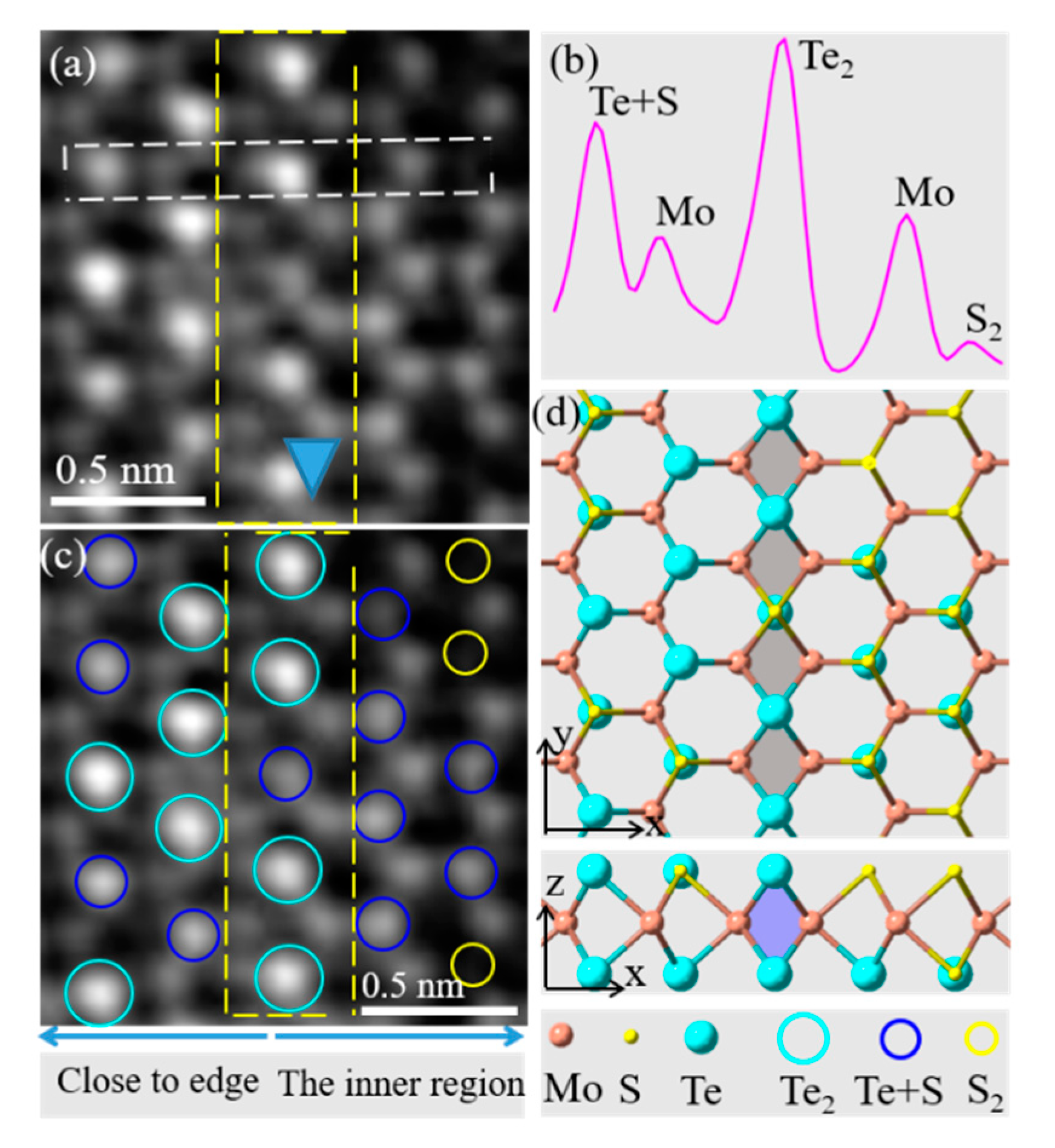
3. Results and Discussion

The sample morphology of the tellurized MoS2 films was outlined by the low-mag ADF-STEM image in Figure 1a, from which a striking feature was found over all the tellurized MoS2 flakes: all their edges appeared in brighter contrast (arrowed in pink), indicating possible tellurium enrichment around the edges as predicted by the Z-contrast mechanism [3]. A close-up view of the edge area illustrated in Figure 1b confirmed the presence of enriched tellurium dopants around the edge, with their ratio reaching as high as 80% in atomic percentage among all chalcogen lattices. The average lattice parameter of the tellurium-enriched region was determined to be 0.346 nm from direct imaging and the corresponding fast Fourier transform spectrum, a value very close to that of the 2H-MoTe2 of 0.352 nm, indicating that at high tellurium doping ratios up to 80%, quasi-pure 2H-MoTe2 regions formed locally. In contrast, in the interior regions further from the edge of the same MoS2 flakes, tellurium substitutions were rarely observed, further confirming that the tellurium substitution was initiated from the edges.
Here we should note that the preferred substitution of doped tellurium at the edges was not due to the phase separation arising from a miscibility gap. As reported in Reference [29], the calculated critical temperature for complete miscibility of MoS2(1-x)Te2x alloy is 493K, and the doping temperature for tellurium in our experiments was 750 ° C or 850 ° C , namely 1023K or 1123K, and was sufficient for the formation of completely miscible MoS2(1-x)Te2x alloy. The preferred substitution of tellurium at the edges can be attributed to the higher reactivity of the edges compared to that of the basal plane of MoS2 [30,31,32]. Moreover, as reported in Reference [33], the density functional calculations indicated that the absorption energy and substitution barrier at the edges were lower than that in the inner region, which resulted in the preferred substitution at the edges. Then, due to the large lattice mismatch between 2H-MoTe2 and 2H-MoS2, tensile strain was formed in the substituted regions. The substitution barrier further decreased with increasing occupation, indicating a continually enhanced substitution rate (self-promoted) and eventually resulting in the preferred substitution of tellurium at the edges.
More importantly, MTBs (as outlined by the yellow dashed rectangles) were observed in these high-level Te doping edge areas in Figure 1b. Further analysis revealed that these MTBs possessed an average length of ~2 nm, an intersection angle of 60° (or 120°) with each other, and showed a tendency to form a closed triangular loop. The atomic resolution ADF-STEM image and the atomic model showing the atomic structure of a representative MTB are given in Figure 2a,d, from which the configuration of the MTB was assigned to 4|4P. Nevertheless, as shown in Figure 2b, the intensity profile along the white dashed lines in Figure 2a confirmed that the doped tellurium replaced and occupied either one or both of the top and bottom sulfur sublattices, i.e., forming substitutional point defects of (Te+S) or Te2 in the host MoS2 crystal. Here, the substitution of sulfur by tellurium might occur following the pathway revealed by nudged elastic band calculations in Reference [33]. Te atoms first absorb on top of S atoms. Then, the Te atoms lift up the neighboring S atoms, and the Te and S atoms are nearly at the same level. Lastly, the Te atom takes the original position of the neighboring S atom, pushing it to the top of the next neighboring S atom, and the S atom possibly evaporates into the atmosphere under the high temperature. Specifically, at MTBs the S2 sites were mostly replaced with Te2, apart from minor (Te+S). In the region close to the edge of MoS2 flakes at X2 sites were Te2 and (Te+S). In the inner region distant from the edge at X2 sites were (Te+S) and S2, as mapped out for the distribution of doped tellurium in Figure 2c. These findings indicate that the tellurium substitution initiated the MTB from the edge and then extended into the inner part.
Comparative experiments conducted at different doping temperatures further revealed the fact that higher doping temperatures led to higher tellurium doping ratios and MTB density as well. For instance, the average doping ratio increased from ~60% at 750 ° C to ~75% at 850 ° C . Such a relationship also suggests that the formation of MTBs could be directly attributed to the tellurium doping.
We next tried to determine the mechanism for a Te-substitution-induced MTB in monolayer MoS2, as illustrated in Figure 3. During the Te doping reaction, some of the sulfur atoms were substituted by tellurium, preferably for those at and around the edge areas. As the doping ratio increased, significant lattice strain built up and accumulated in the tellurized regions due to the atomic size difference between sulfur and tellurium, as indicated by the green arrows in Figure 3a. In turn, these strains led to an upward gliding of the Mo atomic plane with its motion direction marked by black arrows in Figure 3a (the motion direction has three equivalent crystallographic directions with an intersection angle of 120° with each other, and illustrated in Figure 3a was only one example), followed by the formation of sulfur divacancy lines, similar to previous reports [14,34]. Notably, the accumulated strain also resulted in the removal of Mo atoms and more S atoms, as illustrated in Figure 3b. Such a process was intrinsically different from the previously proposed mechanism where the as-formed MTBs consisted of identical lattice atoms to those in the host 2D matrix (see the detailed analysis in Figure S2) [13,14]. Finally, when more and more sulfur atoms were substituted by tellurium, the mirror twinned domains and 4|4P-Te MTBs were formed, as modeled in Figure 3c. In this case, the number of Mo atoms in lines 1–8 in the high Te doping regions was actually smaller than that in the perfect MoS2, with one Mo atom due to the strain induced by large lattice mismatch.
For the loss of Mo atoms and more S atoms shown in Figure 3b, we consider that there was a large mismatch of up to 11.39% between 2H-MoTe2 (aMoTe2 = 3.52 Å) and 2H-MoS2 (aMoS2 = 3.16 Å) and the area of a triangular MoS2 domain with an edge length of naMoS2 (n = 10) corresponded to a triangular MoTe2 domain with an edge length of naMoTe2 (n = 9), as illustrated in Figure S3. If the interior strain inside the high tellurium doping ratio regions was omitted, Mo atoms and more S atoms should be lost during the formation of an inversion domain induced by tellurium doping, and the formed MTBs could be expected to own eight X2 sites (at X2 sites were mostly Te2), as shown in Figure 3c. Due to the different doping levels, a statistical histogram about the number of X2 sites at MTBs in our experiment is shown in Figure 4, and the mean value was calculated as 8.2, which was very close to the expected value, indicating that the strain due to the large lattice mismatch was the driving force for the formation of MTBs. Herein, for the formation of an MTB, unlike previous reports [13], chalcogen vacancy might not be the unique dominant factor. Such a Te-substitution-induced MTB formation was mainly attributed to the energetic request to reduce the strain and interfacial energy after the substitution of sulfur by tellurium. Moreover, due to the higher doping temperature and the supported graphene film, we also could not observe atomic chains—the Te atoms located in between two neighboring Mo atoms, as reported in Reference [35].

4. Conclusions

In this work, we demonstrated that the chalcogen atom exchange route was effective to induce MTB defects in MoS2 monolayers. Results from ADF-STEM images revealed that the substitution of sulfur by tellurium was initiated at the edge and extended into the inner region. The configuration of these MTBs was determined as 4|4P-Te. According to the analysis of the lattice structure around the MTBs, we proposed a model explaining the formation mechanism, which was regarded as an energy-favored process to reduce the strain upon a high ratio tellurium doping. The engineering of MTBs as functional defects can give the TMD materials exotic properties relative to one-dimensional metallic systems.

Supplementary Materials

The following are available online at https://0-www-mdpi-com.brum.beds.ac.uk/2076-3417/10/14/4758/s1, Figure S1: The heated process of the furnace for the tellurium doping. Figure S2: (a) The atomic resolution ADF-STEM image of an independent inversion domain and the corresponding MTBs. Here, we choose an independent inversion domain for the convenience of the analysis of the change of Mo lattice atoms and it’s the same as that around the edges. As seen, the number of the comprised Mo lattice atoms along the white lines (marked as 1-7, respectively) passing through the inversion domain is one less than that in the perfect MoS2. For example, the number of Mo atoms along line 5 is nine, while it’s ten in the perfect MoS2 lattice. (b) The corresponding atomic model of MTBs formed in MoS2, in which Mo and S atoms are denoted as salmon and yellow spheres, respectively, and the number of Mo atoms along the black line 1-7 passing through the inversion domain was the same as that in the perfect MoS2. Note that the Mo lattice atoms inside the inversion domain are not precisely aligned with some of them sitting upward due to lattice distortion. Figure S3: Schematic illustration showing the area of a triangular MoS2 domain with a side length of naMoS2 (n = 10) is equal to that of a triangular MoTe2 domain with a side length of naMoTe2 (n = 9).

Author Contributions

Data curation, X.J.; Funding acquisition, C.J.; Investigation, M.N.K. and D.L.; Writing—original draft, X.J.; Writing—review & editing, X.J., J.L., and C.J. All authors have read and agreed to the published version of the manuscript.

Funding

This work was financially supported by the National Natural Science Foundation of China under Grant Nos 51772265 and 51761165024, the National Basic Research Program of China under Grant No. 2015CB921004, and the Zhe Provincial Natural Science Foundation under Grant No. D19E020002. The work on electron microscopy was done at the Center of Electron Microscopy of Zhejiang University.

Conflicts of Interest

The authors declare no conflicts of interest.

References

  1. Lin, Z.; Carvalho, B.R.; Kahn, E.; Lv, R.; Rao, R.; Terrones, H.; Pimenta, M.A.; Terrones, M. Defect engineering of two-dimensional transition metal dichalcogenides. 2D Mater. 2016, 3, 022002. [Google Scholar] [CrossRef]
  2. Zhou, W.; Zou, X.; Najmaei, S.; Liu, Z.; Shi, Y.; Kong, J.; Lou, J.; Ajayan, P.M.; Yakobson, B.I.; Idrobo, J.C. Intrinsic structural defects in monolayer molybdenum disulfide. Nano Lett. 2013, 13, 2615–2622. [Google Scholar] [CrossRef] [PubMed]
  3. Hong, J.; Hu, Z.; Probert, M.; Li, K.; Lv, D.; Yang, X.; Gu, L.; Mao, N.; Feng, Q.; Xie, L.; et al. Exploring atomic defects in molybdenum disulphide monolayers. Nat. Commun. 2015, 6, 6293. [Google Scholar] [CrossRef] [PubMed] [Green Version]
  4. Yazyev, O.V.; Louie, S.G. Topological defects in graphene: Dislocations and grain boundaries. Phys. Rev. B 2010, 81, 195420. [Google Scholar] [CrossRef] [Green Version]
  5. Gong, Y.; Lin, J.; Wang, X.; Shi, G.; Lei, S.; Lin, Z.; Zou, X.; Ye, G.; Vajtai, R.; Yakobson, B.I.; et al. Vertical and in-plane heterostructures from WS2/MoS2 monolayers. Nat. Mater. 2014, 13, 1135–1142. [Google Scholar] [CrossRef] [Green Version]
  6. Van der Zande, A.M.; Huang, P.Y.; Chenet, D.A.; Berkelbach, T.C.; You, Y.; Lee, G.H.; Heinz, T.F.; Reichman, D.R.; Muller, D.A.; Hone, J.C. Grains and grain boundaries in highly crystalline monolayer molybdenum disulphide. Nat. Mater. 2013, 12, 554–561. [Google Scholar] [CrossRef] [Green Version]
  7. Huang, Y.L.; Chen, Y.; Zhang, W.; Quek, S.Y.; Chen, C.H.; Li, L.J.; Hsu, W.T.; Chang, W.H.; Zheng, Y.J.; Chen, W.; et al. Bandgap tunability at single-layer molybdenum disulphide grain boundaries. Nat. Commun. 2015, 6, 6298. [Google Scholar] [CrossRef] [Green Version]
  8. Huang, Y.L.; Ding, Z.; Zhang, W.; Chang, Y.H.; Shi, Y.; Li, L.J.; Song, Z.; Zheng, Y.J.; Chi, D.; Quek, S.Y.; et al. Gap states at low-angle grain boundaries in monolayer tungsten diselenide. Nano Lett. 2016, 16, 3682–3688. [Google Scholar] [CrossRef]
  9. Yazyev, O.V.; Louie, S.G. Electronic transport in polycrystalline graphene. Nat. Mater. 2010, 9, 806–809. [Google Scholar] [CrossRef] [Green Version]
  10. Sangwan, V.K.; Jariwala, D.; Kim, I.S.; Chen, K.S.; Marks, T.J.; Lauhon, L.J.; Hersam, M.C. Gate-Tunable memristive phenomena mediated by grain boundaries in single-layer MoS2. Nat. Nanotechnol. 2015, 10, 403–406. [Google Scholar] [CrossRef]
  11. Zhang, Z.; Zou, X.; Crespi, V.H.; Yakobson, B.I. Intrinsic magnetism of grain boundaries in two-dimensional metal dichalcogenides. ACS Nano 2013, 7, 10475–10481. [Google Scholar] [CrossRef] [PubMed] [Green Version]
  12. Deng, D.; Novoselov, K.S.; Fu, Q.; Zheng, N.; Tian, Z.; Bao, X. Catalysis with two-dimensional materials and their heterostructures. Nat. Nanotechnol. 2016, 11, 218–230. [Google Scholar] [CrossRef] [PubMed]
  13. Lin, J.; Pantelides, S.T.; Zhou, W. Vacancy-Induced formation and growth of inversion domains in transition-metal dichalcogenide monolayer. ACS Nano 2015, 9, 5189–5197. [Google Scholar] [CrossRef] [PubMed]
  14. Komsa, H.-P.; Krasheninnikov, A.V. Engineering the electronic properties of two-dimensional transition metal dichalcogenides by introducing mirror twin boundaries. Adv. Electron. Mater. 2017, 3, 1600468. [Google Scholar] [CrossRef] [Green Version]
  15. Barja, S.; Wickenburg, S.; Liu, Z.-F.; Zhang, Y.; Ryu, H.; Ugeda Miguel, M.; Hussain, Z.; Shen, Z.-X.; Mo, S.-K.; Wong, E.; et al. Charge density wave order in 1D mirror twin boundaries of single-layer MoSe2. Nat. Phys. 2016, 12, 751–756. [Google Scholar] [CrossRef] [Green Version]
  16. Ma, Y.; Diaz, H.C.; Avila, J.; Chen, C.; Kalappattil, V.; Das, R.; Phan, M.H.; Cadez, T.; Carmelo, J.M.; Asensio, M.C.; et al. Angle resolved photoemission spectroscopy reveals spin charge separation in metallic MoSe2 grain boundary. Nat. Commun. 2017, 8, 14231. [Google Scholar] [CrossRef]
  17. Jolie, W.; Murray, C.; Weiß, P.S.; Hall, J.; Portner, F.; Atodiresei, N.; Krasheninnikov, A.V.; Busse, C.; Komsa, H.-P.; Rosch, A.; et al. Tomonaga-Luttinger liquid in a box: Electrons confined within MoS2 mirror-twin boundaries. Phys. Rev. X 2019, 9, 011055. [Google Scholar] [CrossRef] [Green Version]
  18. Liu, H.; Jiao, L.; Yang, F.; Cai, Y.; Wu, X.; Ho, W.; Gao, C.; Jia, J.; Wang, N.; Fan, H.; et al. Dense network of one-dimensional midgap metallic modes in monolayer MoSe2 and their spatial undulations. Phys. Rev. Lett. 2014, 113, 066105. [Google Scholar] [CrossRef] [Green Version]
  19. Jiao, L.; Liu, H.J.; Chen, J.L.; Yi, Y.; Chen, W.G.; Cai, Y.; Wang, J.N.; Dai, X.Q.; Wang, N.; Ho, W.K.; et al. Molecular-Beam epitaxy of monolayer MoSe2: Growth characteristics and domain boundary formation. New J. Phys. 2015, 17, 053023. [Google Scholar] [CrossRef]
  20. Ma, Y.; Kolekar, S.; Coy Diaz, H.; Aprojanz, J.; Miccoli, I.; Tegenkamp, C.; Batzill, M. Metallic twin grain boundaries embedded in MoSe2 monolayers grown by molecular beam epitaxy. ACS Nano 2017, 11, 5130–5139. [Google Scholar] [CrossRef]
  21. Coelho, P.M.; Komsa, H.-P.; Coy Diaz, H.; Ma, Y.; Krasheninnikov, A.V.; Batzill, M. Post-Synthesis modifications of two-dimensional MoSe2 or MoTe2 by incorporation of excess metal atoms into the crystal structure. ACS Nano 2018, 12, 3975–3984. [Google Scholar] [CrossRef] [PubMed]
  22. Ma, Q.; Isarraraz, M.; Wang, C.S.; Preciado, E.; Klee, V.; Bobek, S.; Yamaguchi, K.; Li, E.; Odenthal, P.M.; Nguyen, A.; et al. Postgrowth tuning of the bandgap of single-layer molybdenum disulfide films by sulfur/selenium exchange. ACS Nano 2014, 8, 4672–4677. [Google Scholar] [CrossRef] [PubMed]
  23. Li, H.; Duan, X.; Wu, X.; Zhuang, X.; Zhou, H.; Zhang, Q.; Zhu, X.; Hu, W.; Ren, P.; Guo, P.; et al. Growth of alloy MoS(2x)Se2(1−x) nanosheets with fully tunable chemical compositions and optical properties. J. Am. Chem. Soc. 2014, 136, 3756–3759. [Google Scholar] [CrossRef]
  24. Feng, Q.; Mao, N.; Wu, J.; Xu, H.; Wang, C.; Zhang, J.; Xie, L. Growth of MoS2(1−x)Se2x (x = 0.41–1.00) monolayer alloys with controlled morphology by physical vapor deposition. ACS Nano 2015, 9, 7450–7455. [Google Scholar] [CrossRef] [PubMed]
  25. Duan, X.; Wang, C.; Fan, Z.; Hao, G.; Kou, L.; Halim, U.; Li, H.; Wu, X.; Wang, Y.; Jiang, J.; et al. Synthesis of WS2xSe2−2x alloy nanosheets with composition-tunable electronic properties. Nano Lett. 2016, 16, 264–269. [Google Scholar] [CrossRef]
  26. Ye, F.; Lee, J.; Hu, J.; Mao, Z.; Wei, J.; Feng, P.X. Environmental instability and degradation of single- and Few-Layer WTe2 nanosheets in ambient conditions. Small 2016, 12, 5802–5808. [Google Scholar] [CrossRef] [Green Version]
  27. Mirabelli, G.; McGeough, C.; Schmidt, M.; McCarthy, E.K.; Monaghan, S.; Povey, I.M.; McCarthy, M.; Gity, F.; Nagle, R.; Hughes, G.; et al. Air sensitivity of MoS2, MoSe2, MoTe2, HfS2, and HfSe2. J. Appl. Phys. 2016, 120, 125102. [Google Scholar] [CrossRef] [Green Version]
  28. Zhu, D.; Shu, H.; Jiang, F.; Lv, D.; Asokan, V.; Omar, O.; Yuan, J.; Zhang, Z.; Jin, C. Capture the growth kinetics of CVD growth of two-dimensional MoS2. npj 2D Mater. Appl. 2017, 1, 8. [Google Scholar] [CrossRef]
  29. Kang, J.; Tongay, S.; Li, J.; Wu, J. Monolayer semiconducting transition metal dichalcogenide alloys: Stability and band bowing. J. Appl. Phys. 2013, 113, 143703. [Google Scholar] [CrossRef] [Green Version]
  30. Fang, Q.; Zhang, Z.; Ji, Q.; Zhu, S.; Gong, Y.; Zhang, Y.; Shi, J.; Zhou, X.; Gu, L.; Wang, Q.; et al. Transformation of monolayer MoS2 into multiphasic MoTe2: Chalcogen atom-exchange synthesis route. Nano Res. 2017, 10, 2761–2771. [Google Scholar] [CrossRef]
  31. Yun, S.J.; Han, G.H.; Kim, H.; Duong, D.L.; Shin, B.G.; Zhao, J.; Vu, Q.A.; Lee, J.; Lee, S.M.; Lee, Y.H. Telluriding monolayer MoS2 and WS2 via alkali metal scooter. Nat. Commun. 2017, 8, 2163. [Google Scholar] [CrossRef] [PubMed]
  32. Lv, D.H.; Zhu, D.C.; Jin, C.H. Preferential substitution of selenium along the grain boundaries in monolayer MoS2(1−x)Se2x alloy. Acta Phys. Chim. Sin. 2017, 33, 1514–1519. [Google Scholar]
  33. Li, H.; Liu, H.; Zhou, L.; Wu, X.; Pan, Y.; Ji, W.; Zheng, B.; Zhang, Q.; Zhuang, X.; Zhu, X.; et al. Strain-Tuning atomic substitution in two-dimensional atomic crystals. ACS Nano 2018, 12, 4853–4860. [Google Scholar] [CrossRef] [PubMed]
  34. Komsa, H.-P.; Kurasch, S.; Lehtinen, O.; Kaiser, U.; Krasheninnikov, A.V. From point to extended defects in two-dimensional MoS2: Evolution of atomic structure under electron irradiation. Phys. Rev. B 2013, 88, 035301. [Google Scholar] [CrossRef] [Green Version]
  35. Yin, G.; Zhu, D.; Lv, D.; Hashemi, A.; Fei, Z.; Lin, F.; Krasheninnikov, A.V.; Zhang, Z.; Komsa, H.P.; Jin, C. Hydrogen-Assisted post-growth substitution of tellurium into molybdenum disulfide monolayers with tunable compositions. Nanotechnology 2018, 29, 145603. [Google Scholar] [CrossRef]
Figure 1. (a) A low-mag annular dark-field scanning transition electron microscope (ADF-STEM) image showing the morphology of the tellurized MoS2 sample. All the edge areas (arrowed in pink) appear brighter than their interior parts. (b) A magnified ADF-STEM image showing the atomic structure of a typical edge area after Te doping. The 4|4P-Te mirror twin boundaries (MTBs) are mapped out in the yellow dashed rectangles. (c) An image of the corresponding fast Fourier transformation spectrum (FFT) of (b), where the first-order diffraction spectra of 2H-MoTe2 and 2H-MoS2 are marked with blue and yellow dashed lines, respectively.
Applsci 10 04758 g001
Figure 2. (a) A typical atomic resolution ADF-STEM image of the 4|4P-Te MTB with its atomic model shown in (d), in which the top image is the top view of the atomic model, and the bottom is the side view. (b) The intensity profile along white dashed lines in (a). (c) The spatial distribution of doped tellurium.
Applsci 10 04758 g002
Figure 3. The atomic models of possible mechanisms forming an inversion domain and MTB. Mo, S, and Te are denoted by the salmon, yellow, and blue spheres, respectively. (a) The substitution of some S atoms by Te. The green arrows represent the compressive strain. The gilding of the Mo atom plane followed by the loss of S atoms to form S divacancy lines. (b) The loss of some Mo and more S atoms to further relax the strain. (c) More S atoms were substituted by Te and the formation of an inversion domain and MTB.
Applsci 10 04758 g003
Figure 4. The histogram of the number of X2 (S2, S+Te, or Te2) sites inside the MTBs. The derived mean value is 8.2, which is very close to the expected value of 8.
Applsci 10 04758 g004

