Review

Self-Organized Conductive Gratings of Au Nanostripe Dimers Enable Tunable Plasmonic Activity

by
Maria Caterina Giordano
1,
Matteo Barelli
1,
Giuseppe Della Valle
2 and
Francesco Buatier de Mongeot
1,*
1
Dipartimento di Fisica, Università di Genova, Via Dodecaneso, 33-16146 Genova, Italy
2
Dipartimento di Fisica and IFN-CNR, Politecnico di Milano, Piazza Leonardo da Vinci, 32-20133 Milano, Italy
*
Author to whom correspondence should be addressed.
Submission received: 17 January 2020 / Revised: 6 February 2020 / Accepted: 10 February 2020 / Published: 14 February 2020

Abstract

:
Plasmonic metasurfaces based on quasi-one-dimensional (1D) nanostripe arrays are homogeneously prepared over large-area substrates (cm2), exploiting a novel self-organized nanofabrication method. Glass templates are nanopatterned by ion beam-induced anisotropic nanoscale wrinkling, enabling the maskless confinement of quasi-1D arrays of out-of-plane tilted gold nanostripes, behaving as transparent wire-grid polarizer nanoelectrodes. These templates enable the dichroic excitation of localized surface plasmon resonances, easily tunable over a broadband spectrum from the visible to the near- and mid-infrared, by tailoring the nanostripes’ shape and/or changing the illumination conditions. The controlled self-organized method allows the engineering of the nanoantennas’ morphology in the form of Au-SiO2-Au nanostripe dimers, which show hybridized plasmonic resonances with enhanced tunability. Under this condition, superior near-field amplification is achievable for the excitation of the hybridized magnetic dipole mode, as pointed out by numerical simulations. The high efficiency of these plasmonic nanoantennas, combined with the controlled tuning of the resonant response, opens a variety of applications for these cost-effective templates, ranging from biosensing and optical spectroscopies to high-resolution molecular imaging and nonlinear optics.

1. Introduction

Plasmonic nanoantennas have collected a strong research and technological interest within the last decade, due to their unique capability to achieve resonant light scattering and near-field confinement at the nanoscale level, enabling novel functionalities in nano-optics, biosensing and energy harvesting [1,2,3,4,5,6,7,8]. In particular, the possibility to tune localized plasmon resonances of subwavelength noble metal nanostructures over a broadband spectrum has been investigated for the selection and local amplification of weak molecular signals in linear and/or nonlinear optical spectroscopies [2,6,7,8,9,10,11,12]. One possibility for the nanofabrication of highly sensitive biosensing templates and nanodevices is given by lithographic techniques, which allow the increased complexity of the individual meta-atoms, controlling the shape and/or the inter-particle spacing at the nanoscale level [13,14,15,16]. The lithographic design of complex in-plane nanoantennas has been exploited to achieve strong efficiency in plasmon-enhanced optical spectroscopies active over different spectral ranges, such as Surface Enhanced Raman Scattering (SERS) [17,18,19,20,21] and Surface Enhanced Infrared Absorption (SEIRA) spectroscopy [11,22,23,24]. Despite the high degree of control provided by the lithographic methods, the reduced patterned areas, limited at the micrometric scale, and/or the multi-step, time-consuming processes strongly hinder the effective application of optimized plasmonic metasurfaces in cost-effective optoelectronic, biosensing and/or diagnostic devices [25,26]. On the other hand, self-assembled nanofabrication methods [27,28,29] allow the large-area functionalization of surfaces, but are generally characterized by low homogeneity and the limited possibility of tailoring the nanostructure’s shape.
Here, large-area (cm2) highly ordered plasmonic templates are prepared by a novel maskless self-organized nanofabrication method. A nanoscale wrinkling instability in glasses induces quasi-1D nanopatterned templates, which enable the confinement of out-of-plane tilted plasmonic nanostripes and/or nanostripe dimers [30]. The method allows the easy tailoring of the nanostripes’ morphology, and thus the tuning of their localized plasmon resonances across the visible (VIS) and near-infrared (IR) spectrum. Most interestingly, our technique enables the engineering of Au-SiO2-Au nanostrip dimers supporting hybridized plasmon resonances [31]. A strong sub-radiant near-field confinement can therefore be achieved by exciting the hybridized magnetic dipole mode, with the additional possibility to tune its resonance over a broadband VIS and near-IR spectrum. The possibility to effectively tailor the nanoscale morphology—thus achieving a fine tuning of the optical response in a cost-effective way—combined with the superior plasmonic near-field confinement and light scattering properties, opens a variety of applications for these templates in optical spectroscopy, biosensing, optical microscopy and nonlinear optics.

2. Results and Discussion

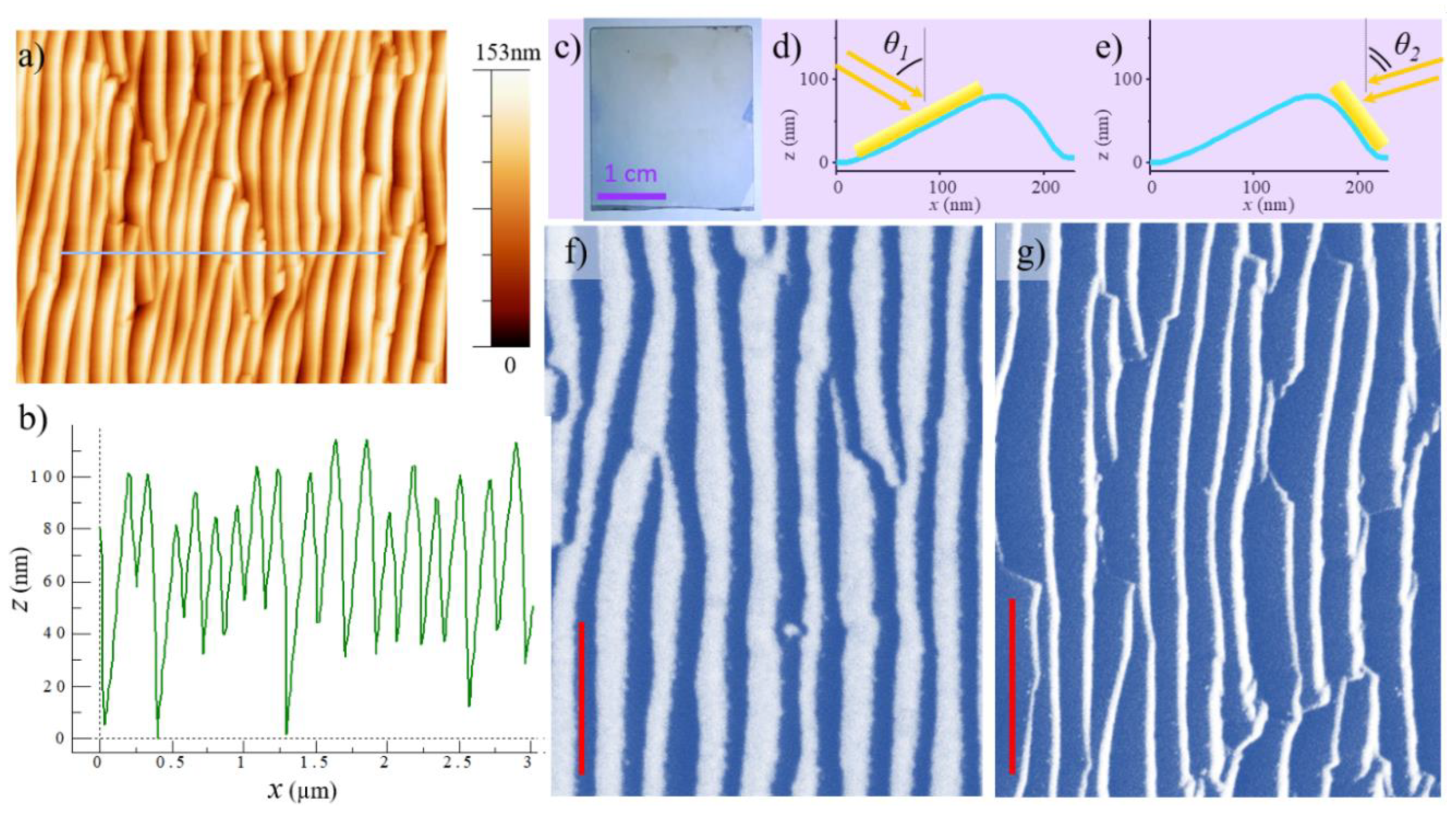
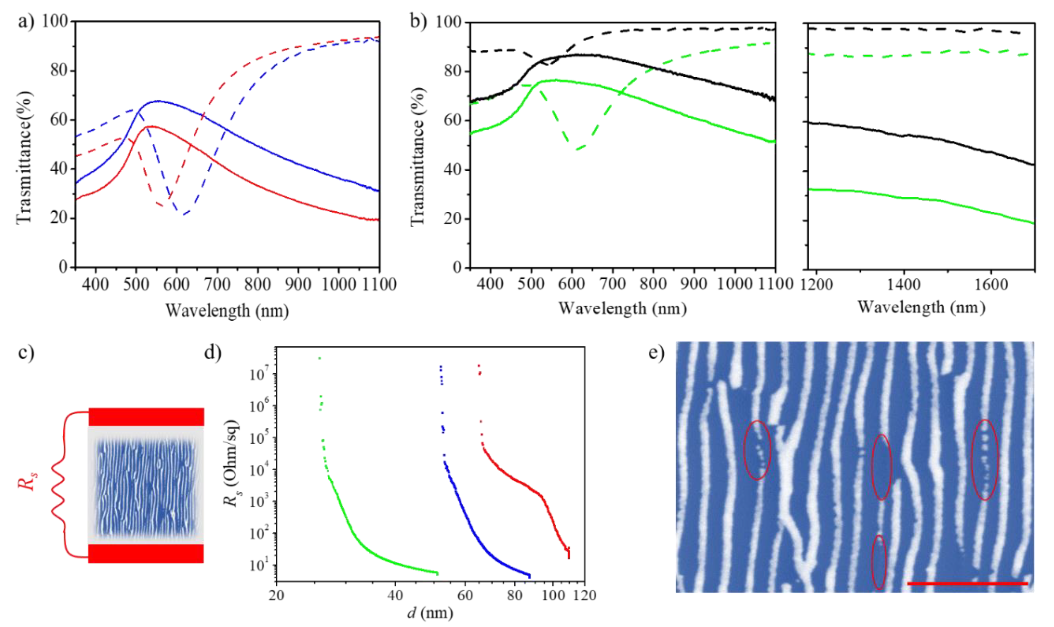
2.1. Plasmonic and Conductive Nanostripe Arrays

Quasi-one dimensional (1D) nanopatterns are homogenously prepared at the glass surface by anisotropic nanoscale wrinkling. High-aspect-ratio subwavelength nanoripples extending over a large area (cm2) can be fabricated by a defocused ion beam irradiation performed near the glass transition temperature (see Supporting Information for experimental details). Periodic quasi-1D nanoripples as long as several micrometers and characterized by a mean height of about 80 nm are shown in Figure 1a,b (AFM topography and cross section profile). The rippling mechanism drives the peculiar growth of facets at the amorphous surface, which are asymmetrically tilted out of plane [30,32], as sketched by the in-scale cross-section profiles of Figure 1d,e. In particular, the ridges directly exposed to the ion beam irradiation exhibit typical slopes of α exceeding 50°, while the opposite show highly defined orientation at about 30° (Supporting Information, Figure S1). This morphology enables the maskless and homogenous confinement of metallic nanostripes whose geometrical configuration can be tailored by changing the Au-illuminated ridges and/or the metal dose over large-area templates (several cm2, as shown by the sample picture in Figure 1c and by the SEM images in Figure S2 of Supporting Information). Two representative examples are shown in the Scanning Electron Microscopy (SEM) images of Figure 1f,g, corresponding to Au growth on the wider facets (tilt of about 30°) and on the smaller ones (tilt of about 50°) [31]. Glancing angle Au evaporation has here been performed at θ1 = 50° (Figure 1h,f) and at θ2 = 70° (Figure 1e–g), respectively, enabling the growth of laterally disconnected Au nanostripes as long as several micrometers on the metal-illuminated facets. The local thickness of the nanostripes reading h = t0 × cos (θα) has been here fixed at 22 nm, while their characteristic width w has been tailored from about 105 nm (Figure 1f) to about 85 nm (Figure 1g), as imposed by the underlying pattern and the metal deposition angle. The high-resolution SEM images highlight the subwavelength lateral disconnection of the nanostripes, while the longitudinal continuity is preserved even at the inter-ripples defect points. Under this condition, strongly anisotropic optical and electrical behavior is expected.
The optical response of these arrays has been probed via far-field extinction spectroscopy across the near-UV, VIS and near-IR spectrum by using a broadband light source collimated over a macroscopic optical spot (diameter of about 3 mm), polarized either longitudinally or transversely, with respect to the major axis of the nanostripes.
The optical transmission spectra of both wide nanostripes (Figure 2a) and narrow steeper stripes (Figure 2b) are strongly dichroic, showing the optical response typical of a continuous film under longitudinal polarization (TE-pol, continuous lines) and behaving as plasmonic nanoantennas under transversal polarization (TM-pol, dashed lines). In the first case (Figure 2a), the optical response has been modulated by confining Au nanostripes of thickness h = 22 nm (blue curves) and h = 30 nm (red curves) by evaporation at the incidence angle θ1 = 50° (Figure 1f). For TE-polarization, the spectral response of these gratings is characterized by a maximum 530 nm wavelength due to the onset of Au inter-band transitions at higher energies, while the transmittance gradually decreases above 560 nm, corresponding to increasing reflectance at lower energies. Conversely, for transversal polarization with respect to the nanostripes (TM), a narrow-band transmission minimum is detected in the VIS spectrum (dashed blue and red curve) due to the excitation of a localized surface plasmon (LSP) resonance in the nanostripe antennas. The change of the nanoantennas’ shape with an increase of the aspect ratio h/w from 0.21 to 0.28 induces a blue shift of the LSP from 615 nm (blue curve, h = 22 nm) to 560 nm (red curve, h = 30 nm). In parallel, a decrease of the full width half maximum of the plasmonic extinction is observed, despite equivalent underlying templates having been exploited in the two cases. Out of resonance, a strong amplification of the TM transmittance with respect to the TE intensity is detected, confirming that the nanostripe arrays behave as broadband wire grid polarizers from the near-UV to the IR spectral range. In particular, the NIR extinction ratio r = TTM/TTE of these Au nanostripes array reads about 4.8 at a 1096 nm wavelength, and even better performances are expected in the red-shifted part of the spectrum. Provided the high degree of order of the gratings, the detected plasmonic behavior is in full agreement with the optical response of corresponding 1D gratings calculated via finite element method simulations [31].
Alternatively, the optical response of these templates can be modulated by performing Au evaporation on the narrower facets (Figure 1e,g). Under this condition, the template imposes a reduction of the antennas’ width in the range of 80 nm, with a possibility to finely tailor this parameter by changing the metal evaporation angle (θ2). The optical response of the quasi-1D array obtained for θ2, respectively fixed at 50° (green curves) and 70° (black curves), is shown in Figure 2b for the near-UV, VIS and near-IR spectrum, and detected up to a 1800 nm wavelength. In analogy to the wider nanostripe samples, a narrow-band plasmonic resonance is detected under TM-polarized illumination (dashed curves), which blue-shifts from 620 nm to 540 nm wavelengths as a consequence of the increase of the aspect ratio (i.e., a decrease of w) under more grazing Au growth. Remarkably, a strong dichroism is detected in the near-IR spectral range, where the transparency exceeds the 90% for transversal polarization (TM), while is attenuated in the range of 20%–40% for TE polarization at about a 1600 nm wavelength. The latter behavior is due to the high reflectivity of the film along the non-resonant polarization, suggesting the possibility of achieving a macroscopic electrical transport parallel to the nanostripes’ long axis.
The possibility to combine high electrical conductivity with optical dichroism has been probed by measuring the longitudinal sheet resistance of the arrays, Rs, as schematically shown in Figure 2c. The longitudinal sheet resistance (Figure 2d) has been measured over a macroscopic circuit of 5×5 mm2 size during Au growth in three different samples, where plasmonic nanostripes were confined on the narrow, steep ridges (as sketched in Figure 1e) at the incidence angle θ2 of 50° (green dots), 60° (blue dots) and 70° (red dots), respectively. The plots show Rs as a function of the Au thickness, d, deposited on the glass facets, and reveal that electrical percolation takes place for all three depositions. The onset of the electrical continuity occurs at 23 nm, 56 nm and 66 nm for growth performed at 50°, 60° and 70°, respectively. At the early stages of the process, geometrical shadowing at the inter-ripples defects, more pronounced under grazing growth, limits the electrical connection between consecutive nanostripes. This effect is well demonstrated by the SEM image of Figure 2e, corresponding to thin Au nanostripes grown under grazing incidence evaporation (θ2 = 80°). Local interruption of the nanostripes is observed in correspondence with the confinement of locally disconnected Au nanoclusters, due to the pronounced shadowing effect from the defect regions at the ripple ends (see red circles in Figure 2e). The macroscopic electrical transport observed in the sheet resistance measurements (Figure 2d) corresponds to the condition of local percolation between micrometric nanostripes at the inter-ripples’ defect regions. Under this condition, a drop of the sheet resistance is observed, followed by a power law decrease, which is as expected for percolative systems [33,34]. Remarkably, very low sheet resistance values, in the range of few Ohm/sq, were measured for all three samples. Under these conditions, the nanoelectrodes behave as wire grid polarizers [35] in the near-IR spectrum, with the transversal transmittance exceeding 80%, while the longitudinal one is attenuated below 10%, at a wavelength of above 950 nm. The good electrical transport of the self-organized nanostripe antennas [36] represents a relevant property of these large-area metamaterials in view of the implementation of plasmonic nanodevices for biosensing, nano-optics and/or photon-harvesting applications.

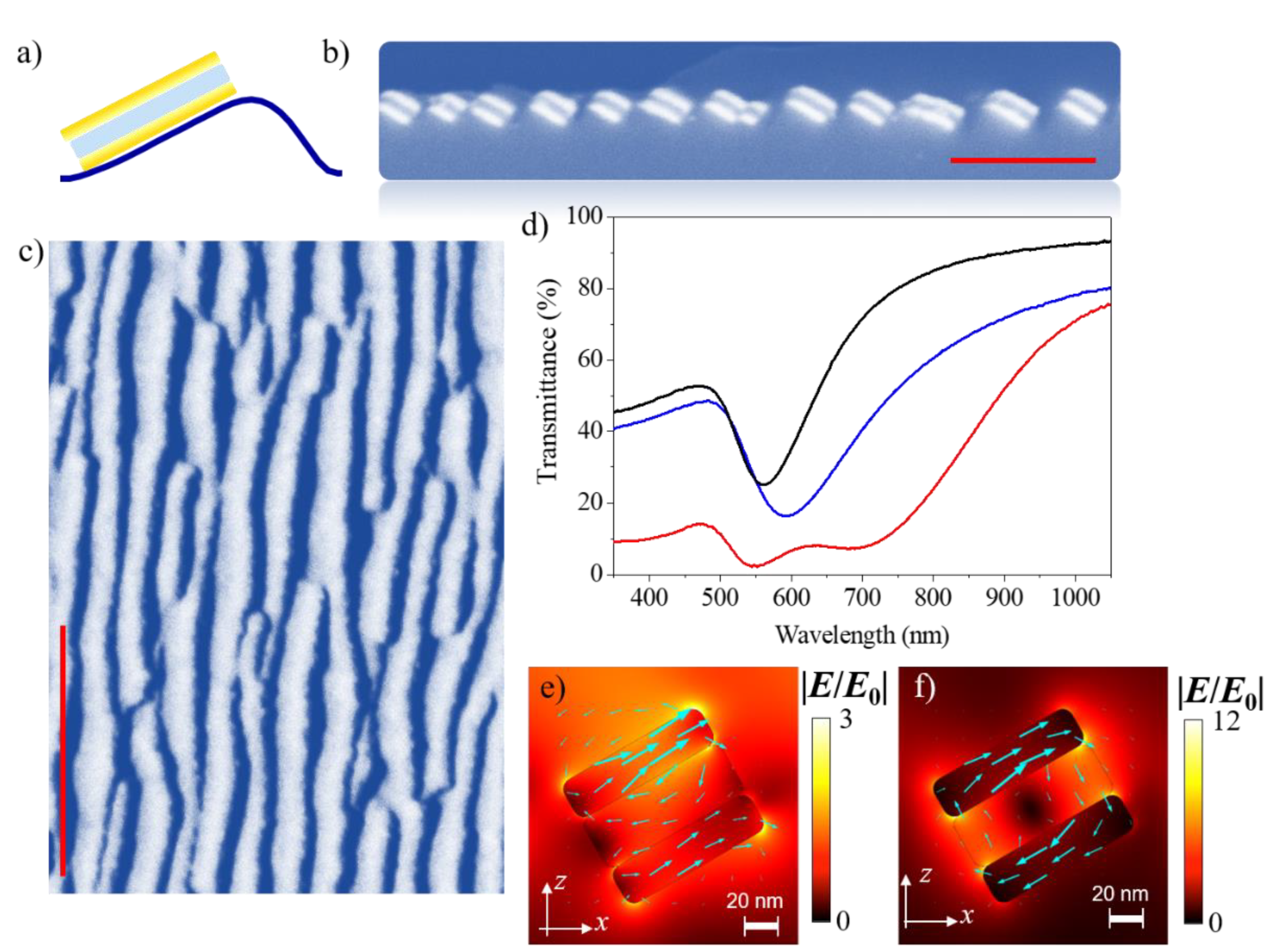
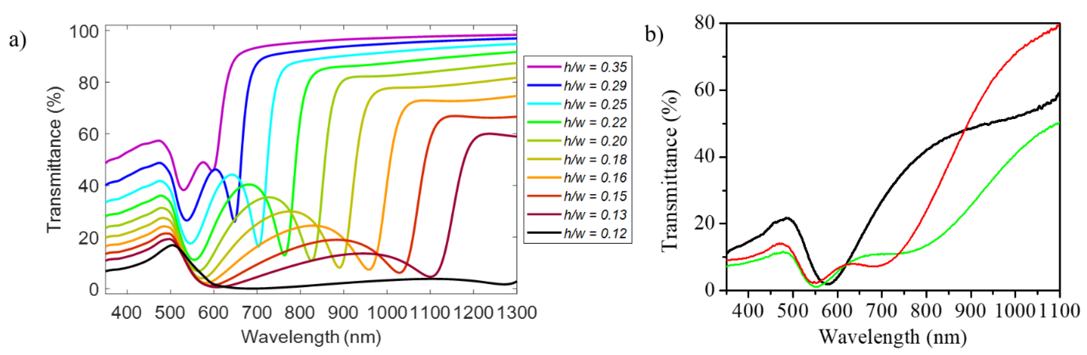
2.2. Plasmon Hybridization in Nanostripe Dimer Arrays

The control enabled by the self-organized nanofabrication process allowed us to develop a multi-step approach for increasing the complexity of the plasmonic nanoantennas, while still preserving the large area homogeneity of the sample. The isolated nanostripes have been vertically stacked, forming tilted nanostripe dimers which feature plasmon hybridization due to the near field coupling between the individual nanoantenna elements.
This has been achieved by selectively coating the tilted Au nanostripes with a SiO2 layer confined at a glancing angle (Figure 3a) by RF magnetron sputtering from an SiO2 target, followed by a further Au deposition step. Under this condition, laterally disconnected Au-SiO2-Au nanodimers are formed in register with the underlying nanopatterned template, as demonstrated by the SEM image of Figure 3b. The top-view SEM image (Figure 3c) clearly shows that the lateral disconnection of the nanodimers is still preserved, thus obtaining homogeneous quasi-1D arrays over large areas. Such tailored nanoscale morphology strongly affects the optical properties of these templates, as shown in Figure 3d. The plot represents the evolution of the optical transmittance detected for TM illumination during the growth of dimer nanoantenna arrays (w = 105 nm, thickness of the Au and of the SiO2 layer reading h = 30 nm and d = 44 nm, respectively). The strong dichroism and the plasmonic excitation characteristic of the single nanostripe configuration (black spectrum) is preserved after the silica growth (blue spectrum), which is slightly red shifted from a 560 nm to 591 nm wavelength, due to the increase of the average refractive index of the dielectric medium. Since by sputtering deposition we confined a non-stoichiometric SiOx film, the effective refractive index of the layer can be calculated considering the measured optical absorption of the bare SiOx film. In the present case, a refractive index of about 1.75 has been evaluated. Interestingly, a splitting of the plasmonic resonance, i.e., plasmon hybridization, is observed when the second Au nanostripe layer is deposited (red curve). A blue-shifted electric dipole (ED) mode is here excited at 550 nm, while a red-shifted magnetic dipole (MD) mode is detected at 700 nm. The extinction spectrum shows a narrow-band ED mode, while a broadening of the MD mode is observed due to the high sensitivity of this resonance to slight variations of the parameters from the individual nanostrip dimers of the array (which is inherent to the self-organization process) [31].
The figure of merit of the hybridized configuration in the near field regime has been evaluated by FEM calculations, revealing a strong sensitivity in the subradiant response of the nanostripe dimers. The electric near-field distribution at resonance is shown in Figure 3e,f for the case of tilted nanostripe dimers excited in resonance with the ED and in the MD mode, respectively. The near-field simulations clearly show a plasmonic near field enhancement in proximity of the nanostripe edges, with field enhancement factors |E/E0| at the single nanostripe edges amounting to about eight. In the case of the nanostripe dimers, we calculate |E/E0| of about 3.5 for ED mode excitation, while a strong enhancement of 19 is observed in the case of MD mode excitation. This characteristic feature clearly evidences the advantage of the nanostripe dimer configuration under MD mode excitation, in view of highly sensitive linear and nonlinear spectroscopies where superior plasmonic amplification factors are required.
In order to prove the capability of the method to tailor on demand the resonant wavelength of the hybridized mode, FEM simulations have been performed either by changing the Au nanostripe aspect ratio h/w in the dimer (Figure 4a) or by changing the thickness of the silica dielectric spacer.
The simulations of Figure 4a clearly show a strong red-shift of the MD mode from about 600 nm to 1300 nm wavelength, as the aspect ratio h/w decreases from 0.35 (violet curve) to 0.12 (black curve), while the spectral position of the ED mode is here weakly dependent on the morphology. In parallel, both the ED and the MD mode are characterized by a pronounced spectral broadening as h/w decreases, with a subsequent reduction of efficiency in terms of field enhancement. Note that this trend in broadening is precisely in line with the hybridization mechanism, according to which the plasmonic resonances of the hybridized system (nanostripe dimer) basically inherit the broadening of the plasmonic resonance of the individual monomers, which for a nanostripe increases with decreasing values of h/w [37,38].
The experimental proof of this behavior is provided by the extinction spectra (Figure 4b), where the tuning of the MD mode is demonstrated by tailoring the shape of the nanostripe dimers. In particular, the width w was fixed at about 105 nm, while the local thickness of the Au or of the silica layer was changed. If the dielectric spacer is kept constant at 44 nm and the Au thickness is reduced from 30 nm (red spectrum) to 22 nm (green spectrum), a softening and red shift of the hybridized plasmonic resonances is detected, as expected based on the theoretical calculations and in line with the theoretical predictions reported in References [37,38]. Indeed, retardation effects determined by thickness-dependent propagation phase shifts strongly affect the longitudinal resonances of single stripe and dimer stripe nanoresonators. In parallel, a strong red shift in the NIR spectrum is observed when the silica thickness decreases to 22 nm (black spectrum in Figure 4b), due to the increase in the coupling strength of the antibonding hybridized nanostripe resonances, which is also in quantitative agreement with the calculated spectra of Figure 4a. An unexpected red shift of the ED mode from 550 nm to 580 nm wavelength is also observed when the thickness of the silica is reduced to 22 nm, which is not in accordance with the pure hybridization model. We attribute this small spectral shift to a change (reduction) of the refractive index of the silica layer in the case of a thinner film, due to a slight difference in the stoichiometry obtained by RF sputtering deposition.

3. Conclusions

We have demonstrated a cost-effective nanofabrication method able to achieve quasi-1D arrays of plasmonic nanostripe antennas, extending homogeneously over a large area (cm2). This self-organized approach enables the tailoring of the nanostripes’ nanoscale morphology, as well as tuning the plasmonic response over a broadband VIS and near-IR spectral range. In parallel, we have shown the possibility to combine high electrical conductivity with strong optical dichroism in semi-transparent nanoelectrodes behaving as wire grid polarizers, thus opening a variety of applications for these templates in active plasmonic devices.
The nanofabrication control characteristic of this self-organized approach has been exploited for developing a multi-step growth of quasi-1D arrays of Au-SiO2-Au nanodimers characterized by hybridized plasmon resonances with superior near field confinement capabilities. This figure, combined with the possibility of tuning the plasmonic modes over a broadband spectrum, opens a variety of applications for these plasmonic metasurfaces in linear and nonlinear optical spectroscopies, advanced microscopy and biosensing.

Supplementary Materials

Author Contributions

F.B.d.M. and G.D.V. conceived the idea, M.C.G. and M.B. performed the experiments, G.D.V. performed the calculations, M.C.G. wrote the original draft of the manuscript and all the authors contributed to the final version of the paper. All authors have read and agreed to the published version of the manuscript.

Funding

This research was funded by Ministero dell’Università e della Ricerca Scientifica (MIUR) through the PRIN 2015 Grant 2015WTW7J3, from Compagnia di San Paolo in the framework of Project ID ROL 9361, and from MAECI in the framework of the Italy-Egypt bilateral protocol.

Acknowledgments

Financial support is gratefully acknowledged from Ministero dell’Università e della Ricerca Scientifica (MIUR) through the PRIN 2015 Grant 2015WTW7J3, from Compagnia di San Paolo in the framework of Project ID ROL 9361, and from MAECI in the framework of the Italy-Egypt bilateral protocol.

Conflicts of Interest

The authors declare no conflict of interest.

References

  1. Schuller, J.A.; Barnard, E.S.; Cai, W.; Jun, Y.C.; White, J.S.; Brongersma, M.L. Plasmonics for extreme light concentration and manipulation. Nat. Mater. 2010, 9, 193–204. [Google Scholar] [CrossRef] [PubMed]
  2. Kneipp, K.; Moskovits, M.; Kneipp, H. Surface Enhanced Raman Scattering: Physics and Applications; Springer: New York, NY, USA, 2006. [Google Scholar]
  3. Yu, N.; Capasso, F. Flat optics with designer metasurfaces. Nat. Mater. 2014, 13, 139–150. [Google Scholar] [CrossRef] [PubMed]
  4. Woessner, A.; Lundeberg, M.B.; Gao, Y.; Principi, A.; Alonso-González, P.; Carrega, M.; Watanabe, K.; Taniguchi, T.; Vignale, G.; Polini, M.; et al. Highly confined low-loss plasmons in graphene–boron nitride heterostructures. Nat. Mater. 2015, 14, 421–425. [Google Scholar] [CrossRef] [PubMed] [Green Version]
  5. Aydin, K.; Ferry, V.E.; Briggs, R.M.; Atwater, H.A. Broadband polarization-independent resonant light absorption using ultrathin plasmonic super absorbers. Nat. Commun. 2011, 2, 517. [Google Scholar] [CrossRef] [PubMed]
  6. Alessandri, I.; Ferroni, M.; Depero, L.E. Plasmonic heating-assisted transformation of SiO 2/Au core/shell nanospheres (Au nanoshells): Caveats and opportunities for SERS and direct laser writing. Plasmonics 2013, 8, 129–132. [Google Scholar] [CrossRef]
  7. Giordano, M.C.; Foti, A.; Messina, E.; Gucciardi, P.G.; Comoretto, D.; De Mongeot, F.B. SERS amplification from self-organized arrays of plasmonic nanocrescents. ACS Appl. Mater. Interf. 2016, 8, 6629–6638. [Google Scholar] [CrossRef]
  8. Belardini, A.; Benedetti, A.; Centini, M.; Leahu, G.; Mura, F.; Sennato, S.; Sibilia, C.; Robbiano, V.; Giordano, M.C.; Martella, C.; et al. Second harmonic generation circular dichroism from self-ordered hybrid plasmonic–photonic nanosurfaces. Adv. Opt. Mater. 2014, 2, 208–213. [Google Scholar] [CrossRef]
  9. Lee, J.; Crampton, K.T.; Tallarida, N.; Apkarian, V.A. Visualizing vibrational normal modes of a single molecule with atomically confined light. Nat. 2019, 568, 78–82. [Google Scholar] [CrossRef]
  10. Belardini, A.; Larciprete, M.C.; Centini, M.; Fazio, E.; Sibilia, C.; Chiappe, D.; Martella, C.; Toma, A.; Giordano, M.; de Mongeot, F.B. Circular dichroism in the optical second-harmonic emission of curved gold metal nanowires. Phys. Rev. Lett. 2011, 107, 257401. [Google Scholar] [CrossRef]
  11. Neubrech, F.; Pucci, A.; Cornelius, T.W.; Karim, S.; García-Etxarri, A.; Aizpurua, J. Resonant plasmonic and vibrational coupling in a tailored nanoantenna for infrared detection. Phys. Rev. Lett. 2008, 101, 157403. [Google Scholar] [CrossRef] [Green Version]
  12. Leahu, G.; Petronijevic, E.; Belardini, A.; Centini, M.; Sibilia, C.; Hakkarainen, T.; Koivusalo, E.; Rizzo Piton, M.; Suomalainen, S.; Guina, M. Evidence of Optical Circular Dichroism in GaAs-Based Nanowires Partially Covered with Gold. Adv. Opt. Mater. 2017, 5, 1601063. [Google Scholar] [CrossRef] [Green Version]
  13. Pors, A.; Nielsen, M.G.; Bozhevolnyi, S.I. Analog Computing Using Reflective Plasmonic Metasurfaces. Nano Lett. 2015, 15, 791–797. [Google Scholar] [CrossRef] [Green Version]
  14. Near, R.; Tabor, C.; Duan, J.; Pachter, R.; El-Sayed, M. Pronounced Effects of Anisotropy on Plasmonic Properties of Nanorings Fabricated by Electron Beam Lithography. Nano Lett. 2012, 12, 2158–2164. [Google Scholar] [CrossRef] [PubMed]
  15. Iorio, A.; Rocci, M.; Bours, L.; Carrega, M.; Zannier, V.; Sorba, L.; Roddaro, S.; Giazotto, F.; Strambini, E. Vectorial Control of the Spin–Orbit Interaction in Suspended InAs Nanowires. Nano Lett. 2018, 19, 652–657. [Google Scholar] [CrossRef] [Green Version]
  16. Giordano, M.C.; Viti, L.; Mitrofanov, O.; Vitiello, M.S. Phase-sensitive terahertz imaging using room-temperature near-field nanodetectors. Optica 2018, 5, 651–657. [Google Scholar] [CrossRef] [Green Version]
  17. Sharma, B.; Frontiera, R.R.; Henry, A.I.; Ringe, E.; Van Duyne, R.P. SERS: Materials, applications, and the future. Materialstoday 2012, 15, 16–25. [Google Scholar] [CrossRef]
  18. Zhang, Y.; Zhen, Y.-R.; Neumann, O.; Day, J.K.; Nordlander, P.; Halas, N.J. Coherent anti-Stokes Raman scattering with single-molecule sensitivity using a plasmonic Fano resonance. Nat. Commun. 2014, 5, 4424. [Google Scholar] [CrossRef]
  19. Gwo, S.; Wang, C.-Y.; Chen, H.-Y.; Lin, M.-H.; Sun, L.; Li, X.; Chen, W.-L.; Chang, Y.-M.; Ahn, H. Plasmonic Metasurfaces for Nonlinear Optics and Quantitative SERS. ACS Photon. 2016, 3, 1371–1384. [Google Scholar] [CrossRef]
  20. Repetto, D.; Giordano, M.C.; Foti, A.; Gucciardi, P.G.; Mennucci, C.; De Mongeot, F.B. SERS amplification by ultra-dense plasmonic arrays on self-organized PDMS templates. Appl. Surf. Sci. 2018, 446, 83–91. [Google Scholar] [CrossRef]
  21. Kessentini, S.; Barchiesi, D.; D’Andrea, C.; Toma, A.; Guillot, N.; Di Fabrizio, E.; Fazio, B.; Maragò, O.M.; Gucciardi, P.G.; De La Chapelle, M.L. Gold Dimer Nanoantenna with Slanted Gap for Tunable LSPR and Improved SERS. J. Phys. Chem. C 2014, 118, 3209–3219. [Google Scholar] [CrossRef]
  22. Wu, C.; Khanikaev, A.B.; Adato, R.; Arju, N.; Yanik, A.A.; Altug, H.; Shvets, G. Fano-resonant Asymmetric Metamaterials for Ultrasensitive Spectroscopy and Identification of Molecular Monolayers. Nat. Mater. 2012, 11, 69–75. [Google Scholar] [CrossRef] [PubMed]
  23. Neubrech, F.; Beck, S.; Glaser, T.; Hentschel, M.; Giessen, H.; Pucci, A. Spatial Extent of Plasmonic Enhancement of Vibrational Signals in the Infrared. ACS Nano 2014, 8, 6250–6258. [Google Scholar] [CrossRef] [PubMed]
  24. Rodrigo, D.; Limaj, O.; Janner, D.; Etezadi, D.; De Abajo, F.J.G.; Pruneri, V.; Altug, H. Mid-infrared Plasmonic Biosensing with Graphene. Science 2015, 349, 165–168. [Google Scholar] [CrossRef] [PubMed] [Green Version]
  25. Yavas, O.; Aćimović, S.S.; Garcia-Guirado, J.; Berthelot, J.; Dobosz, P.; Sanz, V.; Quidant, R. Self-Calibrating On-Chip Localized Surface Plasmon Resonance Sensing for Quantitative and Multiplexed Detection of Cancer Markers in Human Serum. ACS Sens. 2018, 3, 1376–1384. [Google Scholar] [CrossRef] [PubMed]
  26. Aćimović, S.S.; Ortega, M.A.; Sanz, V.; Berthelot, J.; Garcia-Cordero, J.L.; Renger, J.; Maerkl, S.J.; Kreuzer, M.P.; Quidant, R. LSPR Chip for Parallel, Rapid, and Sensitive Detection of Cancer Markers in Serum. Nano Lett. 2014, 14, 2636–2641. [Google Scholar] [CrossRef] [PubMed] [Green Version]
  27. Verre, R.; Fleischer, K.; Ualibek, O.; Shvets, I.V. Self-assembled broadband plasmonic nanoparticle arrays for sensing applications. Appl. Phys. Lett. 2012, 100, 31102. [Google Scholar] [CrossRef] [Green Version]
  28. Repetto, D.; Giordano, M.C.; Martella, C.; De Mongeot, F.B. Transparent aluminium nanowire electrodes with optical and electrical anisotropic response fabricated by defocused ion beam sputtering. Appl. Surf. Sci. 2015, 327, 444–452. [Google Scholar] [CrossRef]
  29. Della Valle, G.; Polli, D.; Biagioni, P.; Martella, C.; Giordano, M.C.; Finazzi, M.; Longhi, S.; Duò, L.; Cerullo, G.; De Mongeot, F.B. Self-organized plasmonic metasurfaces for all-optical modulation. Phys. Rev. B 2015, 91, 235440. [Google Scholar] [CrossRef]
  30. Giordano, M.C.; De Mongeot, F.B. Anisotropic Nanoscale Wrinkling in Solid-State Substrates. Adv. Mater. 2018, 30, 1801840. [Google Scholar] [CrossRef]
  31. Giordano, M.C.; Longhi, S.; Barelli, M.; Mazzanti, A.; De Mongeot, F.B.; Della Valle, G. Plasmon hybridization engineering in self-organized anisotropic metasurfaces. Nano Res. 2018, 11, 3943–3956. [Google Scholar] [CrossRef]
  32. Gnecco, E.; Nita, P.; Casado, S.; Pimentel, C.; Mougin, K.; Giordano, M.C.; Repetto, D.; De Mongeot, F.B. Channeling motion of gold nanospheres on a rippled glassed surface. Nanotechnology 2014, 25, 485302. [Google Scholar] [CrossRef] [PubMed]
  33. Octavio, M.; Gutierrez, G.; Aponte, J. Conductivity and noise critical exponents in thin films near the metal-insulator percolation transition. Phys. Rev. B 1987, 36, 2461. [Google Scholar] [CrossRef] [PubMed]
  34. Giordano, M.C.; Repetto, D.; Mennucci, C.; Carrara, A.; De Mongeot, F.B. Template-assisted growth of transparent plasmonic nanowire electrodes. Nanotechnology 2016, 27, 495201. [Google Scholar] [CrossRef] [PubMed]
  35. Aas, L.M.S.; Kildemo, M.; Martella, C.; Giordano, M.C.; Chiappe, D.; De Mongeot, F.B. Optical properties of biaxial nanopatterned gold plasmonic nanowired grid polarizer. Opt. Express 2013, 21, 30918–30931. [Google Scholar] [CrossRef] [PubMed]
  36. Barelli, M.; Repetto, D.; De Mongeot, F.B. Infrared Plasmonics via Self-Organized Anisotropic Wrinkling of Au/PDMS Nanoarrays. ACS Appl. Polym. Mater. 2019, 1, 1334–1340. [Google Scholar] [CrossRef]
  37. Della Valle, G.; Søndergaard, T.; Bozhevolnyi, S.I. Plasmon-polariton nano-strip resonators: From visible to infra-red. Opt. Express 2008, 16, 6867–6876. [Google Scholar] [CrossRef]
  38. Søndergaard, T.; Jung, J.; Bozhevolnyi, S.I.; Della Valle, G. Theoretical analysis of gold nano-strip gap plasmon resonators. New J. Phys. 2008, 10, 105008. [Google Scholar] [CrossRef]
Figure 1. , (a,b) AFM topography and cross-section line profile of the nanopatterned glass template; (c) Picture of the sample: the plasmonic nanostructures homogeneously extend over large area (cm2); (d,e) sketch of the glancing angle Au evaporation growth on the wide and on the narrow facets, respectively; and (f,g) SEM images of the tilted Au nanostripe arrays grown under condition of panel (d,e), respectively. The red scale bars in panel (f,g) correspond to 500 nm and 1 µm, respectively.
Applsci 10 01301 g001
Figure 2. (a,b) Optical extinction spectra of quasi-1D Au nanostripe arrays confined on the wide and on the narrow facets, respectively, as sketched in Figure 1d,e. The spectra were recorded for the longitudinal (TE-continuous lines) and transversal (TM-dashed lines) polarization of the UV-VIS-NIR illumination beam, with respect to the nanostripes’ long axis. In panel (a) the nanostripes’ aspect ratio h/w was increased from 0.21 (blue spectra) to 0.28 (red spectra), by increasing the height h from 22 nm to 30 nm; in panel (b), h/w was increased from the green to the black curve by decreasing the width of the nanoantennas; (c) sketch of the circuit exploited for measuring the sheet resistance (Rs) parallel to the main axis of the nanostripes (size of the circuit: 2 × 2 mm2); (d) plot of Rs measured in-situ during the growth of Au nanoantennas at θ2 = 50° (green curve), 60° (blue curve) and 70° (red curve) respectively; and (e) SEM image of Au nanostripe arrays confined on the narrow facets under glancing condition (θ2 = 80°): a strong shadowing effect is observed at the inter-ripple connection (red circles) with no gold or disconnected nanoclusters. These regions limit the electrical conductivity at the early stages of the Au evaporation process. The scale bar corresponds to 1 µm.
Applsci 10 01301 g002
Figure 3. (a) Cross-section sketch of the Au-SiO2-Au nanostripe dimers; (b,c) cross-section and top-view SEM image of the nanostripe dimer arrays, respectively. The scale bars correspond to 500 nm and 1 µm, respectively; (d) extinction optical spectra for the TM-polarized excitation of Au nanostripe (black curve), Au-silica (blue curve) and Au-silica-Au nanostripe dimer arrays (red curve). The nanostripes’ width was fixed at about 105 nm, while the local thickness of the Au-silica-Au layers was set at 30-44-30 nm respectively; and (e,f) FEM simulation of the near field distribution for nanostripe dimer excited in resonance with the plasmonic electric- and magnetic-dipole mode (550 nm and 700 nm wavelength), respectively.
Applsci 10 01301 g003
Figure 4. (a) FEM calculations of nanostripe dimers’ optical behavior as a function of the Au nanostripes aspect ratio h/w, which is varied by acting on w and keeping h fixed to 22 nm. The silica spacer is set to 24 nm thickness and the array periodicity is 210 nm; and (b) TM-polarized optical extinction spectra of nanostripe dimer arrays, where the Au-SiO2-Au layers thickness was tailored as follows: 30-44-30 nm (red curve), 22-44-22 nm (green curve) and 22-22-22 nm (black curve).
Applsci 10 01301 g004

