1. Introduction
The arrangements and microstructure are intrinsic properties of materials, especially for metal nano-materials. Recently, ordered metal particle-chains (such as Ag, Au, Cu) which exhibit unique optical properties are widely applied in plasmon waveguides, colour filters, and single molecular devices, etc [
1,
2,
3]. A traditional strategy based on Rayleigh instability has been developed to fabricate one-dimensional particle-chains from their nanowires [
4,
5,
6]. Note that, the liquid state of nanowires is the precondition of Rayleigh instability [
7], and high temperature is generally required to melt these materials. For example, ordered conversion only occurs with high temperature (for Cu 600 °C, Au 500 °C), and a long-time (about 4 to 6 h) [
8,
9], and lead to severely evaporation due to the vacuum or inert gas protection at low pressure. Meanwhile, low temperature (about 0.2 melting points (example: melting point of Ag 961.78 °C, 0.2 × 961.78 °C = 192.356 °C) for grain growth) surface melting induced Rayleigh instability generally causes insufficient or even random fractures of metal nanowires [
10]. The high temperature and long-time needs will no doubt blur the application of Rayleigh instability in the fabrication of ordered metal particle-chains.
Low temperature RF (radio frequency) plasma with highly energetic ions and self-bias properties, can lead to uniform bombarding on material surfaces [
11]. The temperature of RF plasma induced structure modifications, such as the welding of nanowires or nanoflakes into hollow structures, is much lower than that based on heating [
12]. Generally, plasma treating exerted on nanomaterials, such as carbon nanotubes [
13], NiCoP nanoflakes [
14], Co
3O
4 nanowire arrays [
12] mainly exhibits surface roughness increment or surface microstructure deformation, and this is because the plasma bombarding directly offers kinetic energy for the atoms of material surfaces. This phenomenon inspires us that high diffusion capacity of Ag atoms on Ag nanowires surfaces can be obtained by RF plasma treatment. Related to the Rayleigh instability, similarly, ordered metal particle-chains should be obtained from metal nanowires with temperature below 100 °C.
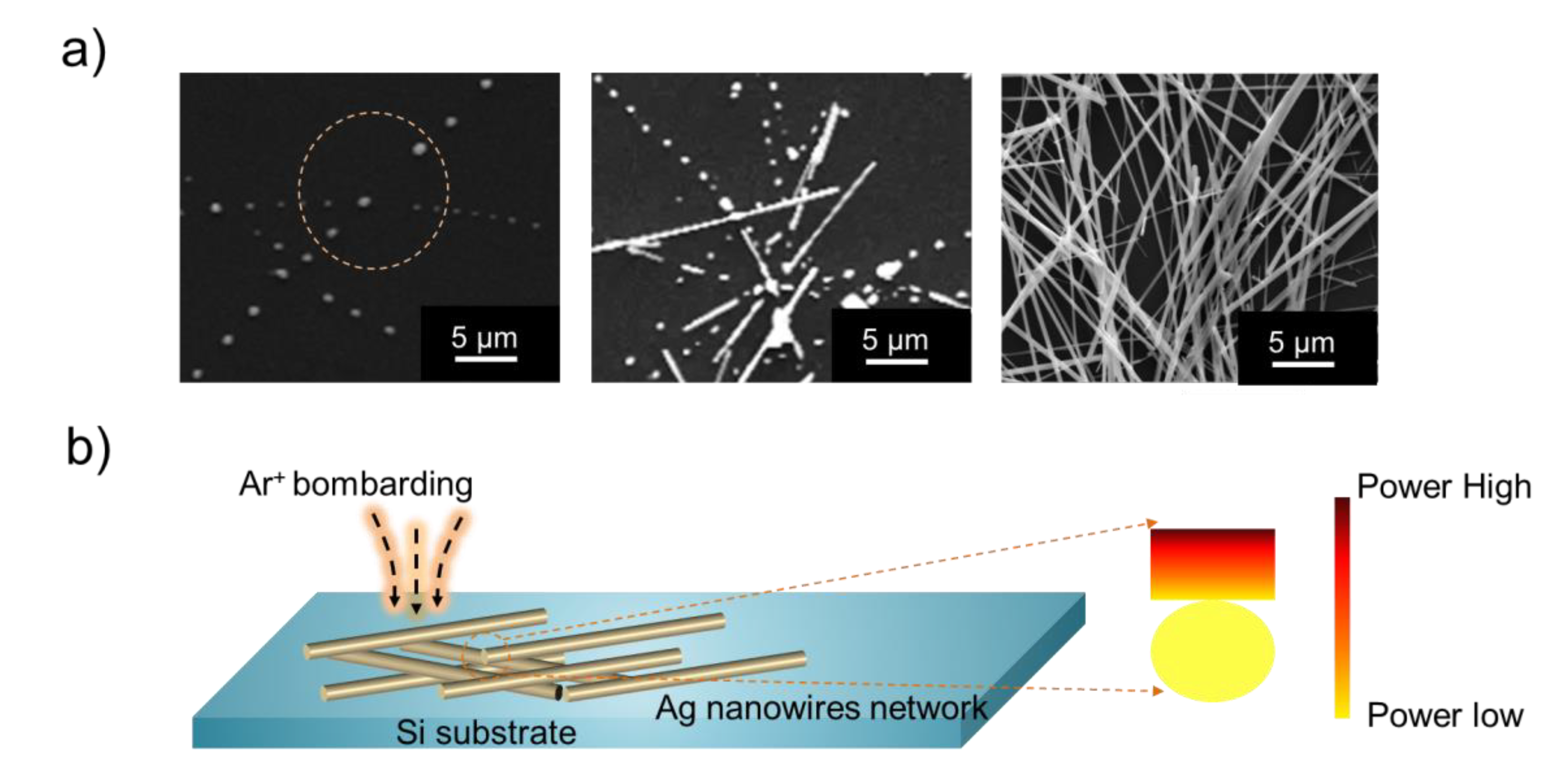
Herein, we adopted Ag nanowires (AgNWs) as example to realize the large-scale fabrication of the ordered particle-chains. The scale of AgNWs films on silicon substrate are about 1–3 cm2. To show the universality of this method, AgNWs with various diameters and aggregations were chosen and then treated by plasma. We found that the dispersed AgNWs with various diameters were nearly completely converted into highly ordered particle-chains deposited on Si substrates on a macro scale with only 3 to 5 min. Additionally, the temperature of the Si substrates was no more than 100 °C during the process. Moreover, similar to the high temperature heat treatment, the periodicity of these particle-chains shows strong dependency on the diameters of AgNWs as expected by Rayleigh instability. Meanwhile, the aperiodicity of particle-chains has been observed as the aggregation of AgNWs begins. Furthermore, wire–wire welding has also been found on AgNWs with the increment of the aggregation.
2. Materials and Methods
AgNWs with diameters ranging from 60 to 300 nm (average 150 nm) and lengths ranging from 10 to 50 µm (average 40 µm) were synthesised by hydrothermal method [
15]. Polyvinyl pyrrolidone (PVP) (molecular mass 360 k) Aladdin (Aladdin reagent (Shanghai) Co., Ltd. Shanghai, China), sodium sulphide and silver nitrate Sinopharm (Sinopharm Group Co. Ltd. Shanghai, China) were mixed in ethylene glycol and put in Teflon-lined stainless autoclaves. AgNWs of various sizes (diameters and lengths) were obtained after 4–7 h under 160 °C. The sizes of AgNWs can be controlled both by reaction time and by temperature. In our case, larger diameter and longer AgNWs can be obtained by prolonging reaction time within 12 h. To remove the adhered PVP layer on AgNWs surfaces, the suspension of AgNWs was treated by ethanol rinse and filtration with five circles. The prepared AgNWs were suspended in ethanol with 0.1 wt%, 0.5 wt% and 3 wt% and were dropped on Si substrates to form dispersed, slightly lapped, and seriously lapped AgNWs respectively. Following this, these samples were dried in a drying oven under 50 °C.
Herein, a tuneable RF system (0–250 W) with frequency of 13.56 MHZ and Ar gas of 0.2 Pa has been used to generate plasma and avoid oxidation on Ag nanowires. The prepared samples have been treated with plasma for various times. In contrast, heat treatments on Ag nanowires under the same Ar gas pressure have also been carried out at a heating rate of 10 °C/min.
The characterizations of sample morphologies were carried out with an optical microscope (OM, ZEISS, Axioplan 2 imaging MOT), a field emission scanning electron microscope (SEM, FEI-Nova Nano SEM 450) and a transmission electron microscope (TEM, JEOL-2100F).
3. Results and Discussion
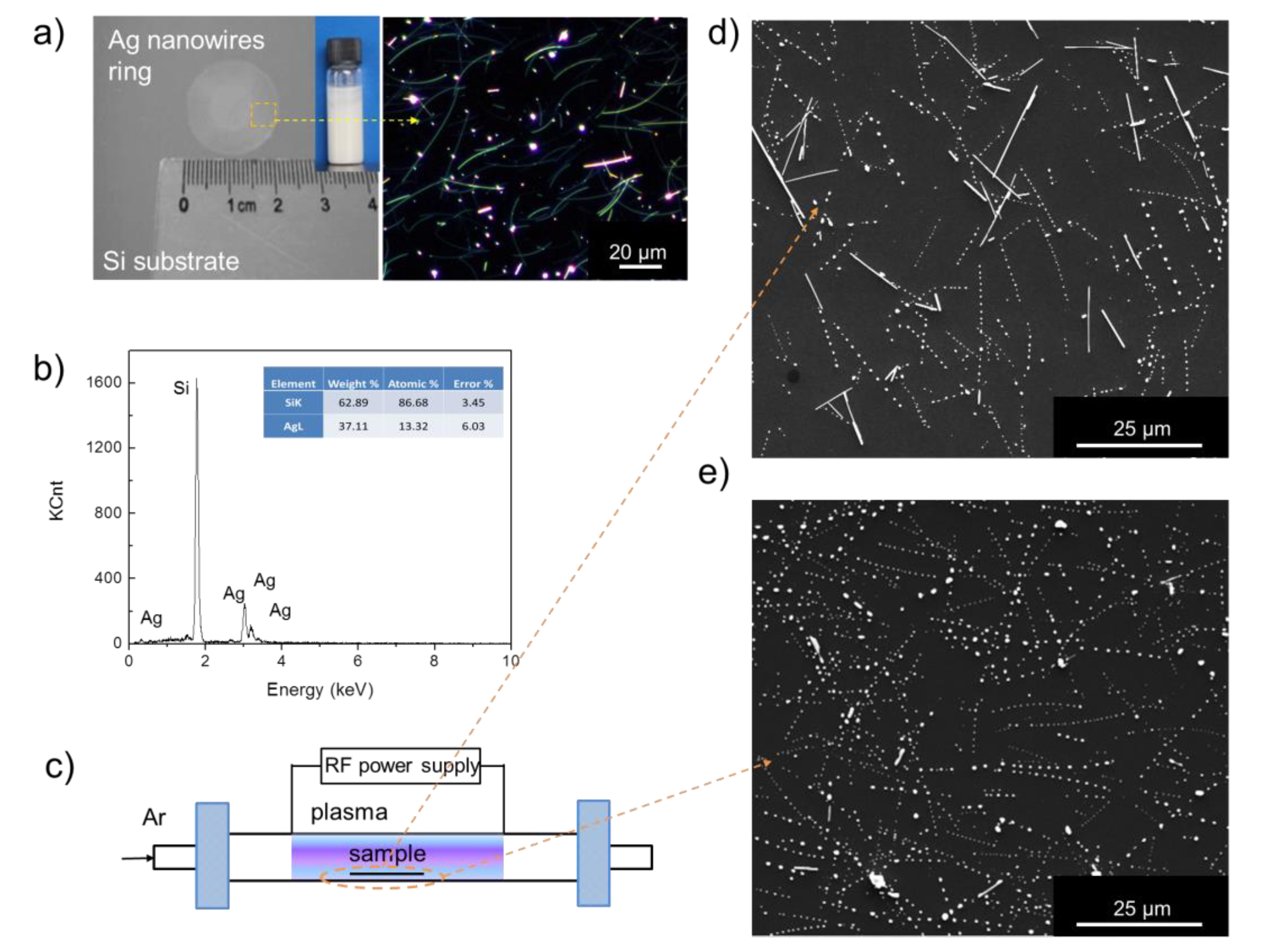
AgNWs were deposited on Si substrates (samples) as thin circle layers (“coffee rings”) due to the natural spreading and drying of their ethanol suspension [
16,
17], as shown in
Figure 1a. From the element analysis, the spreading treatment of ethanol suspension AgNWs deposited on Si substrate is “a clean way” without introducing impurities, as shown in
Figure 1b. This element analysis was exerted on the sample in
Figure 1a. As a result, AgNWs adhered on Si substrate are mainly contributed by weak Van der Waals forces [
16]. Then, the prepared samples were put in a chemical vapour deposition and treated by RF plasma, as shown in
Figure 1c. In our case, 60 W power of RF (Ar
+ average energy with about 10–30 eV, which is around the 15 eV sputtering threshold energy of Ag [
18,
19]) was chosen to exert on samples. Such power of plasma can provide enough kinetic energy on the surfaces of AgNWs and meanwhile avoid sputtering. By 3 min RF plasma treatment, partial breakage occurs to AgNWs, which then converts into uniform particle-chains on a macro scale (
Figure 1d). Furthermore, the centre-to-centre distances between Ag nanoparticles show strong relations with their diameters. Similar phenomenon can be also found on AgNWs after 5 min RF plasma treatment. In contrast to 3 min RF plasma treatment, nearly all AgNWs with various diameters convert to highly ordered particle-chains (
Figure 1e). Apparently, the conversion of AgNWs is more thorough with a little longer treatment. What’s more, the temperature of the Si substrates obtained by a thermocouple (measurement accuracy 0.1 °C) is from room temperature to about 95 °C during the process, which is much lower than the melting point of bulk Ag. Note that the temperature increase in Si substrates are polyphyletic, which can be separated into three parts: 1) heat conduction from AgNWs; 2) heat conduction from equipment; and 3) heat generated on silicon substrate by plasma. Obviously, the heat conduction from AgNWs is the minimum part. The temperature increase cannot simply be evacuated by the test results by the thermocouple. However, the total temperature increment is no more than 80 °C during the whole plasma treatment. As a result, the RF plasma treatment can be deemed as a low temperature way for AgPCs fabrication from AgNWs.
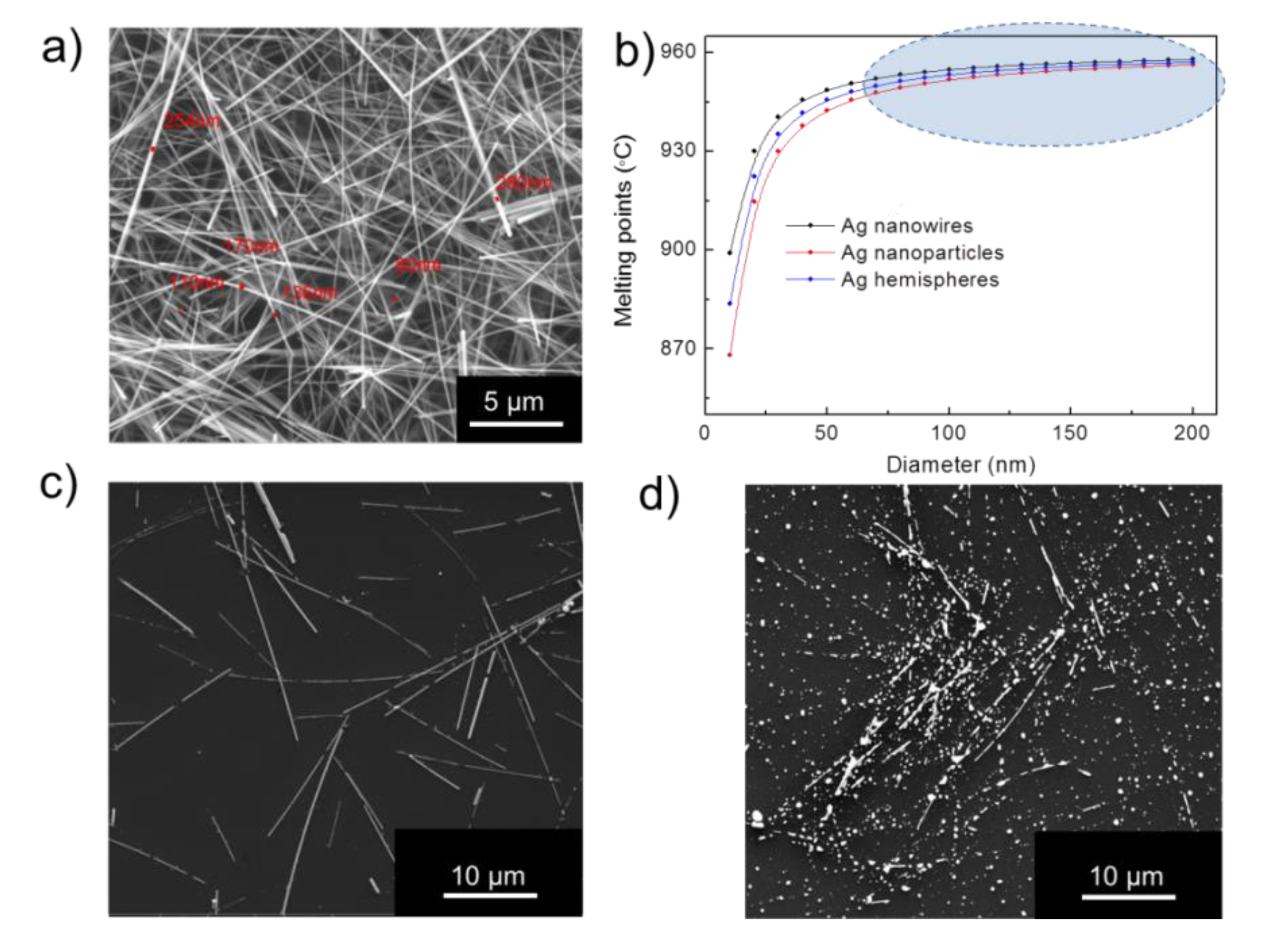
A contrast test based on the traditional heat treatment has been carried out. AgNWs with diameters ranging from about 60 to 300 nm have been adopted in our case, as shown in
Figure 2a. Calculations of melting points (
) of three typical Ag nanostructures (nanowire, hemisphere, and nanoparticle) with various sizes are based on the K. K. Nanda liquid-drop model [
20,
21], which have been presented in
Figure 2b. Furthermore, their melting points can be expressed by
, in which
is the melting point of bulk Ag, the value of
is obtained from the empirical relation,
are their diameters, and
the constant of 2/3, 5/6 and 1 for nanowire, hemisphere, and nanoparticle respectively. For nanostructures with relatively free surfaces, the melting temperature decreases with their size reduction. It can be clearly observed that melting points of all these structures are greater than 930 °C. Owing to the minimum temperature of secondary (or abnormal) grain growth of Ag (about 0.2
), 200 °C heat treatment has been chosen. As reported, no visible change or broken junction points can be observed under 200 °C within 30 min heat treatment [
9]. Even after 6 h, only random and insufficient coarsening on AgNWs can be observed, as shown in
Figure 2c. As the temperature increases to 450 °C, the coarsening grade of AgNWs is much higher than that under 200 °C, as shown
Figure 2d. However, the periodicity of formed Ag particle-chains is still relatively low (a little better than that under 200 °C) under 450 °C with 6 h. In contrast to RF plasma treatment, the conversion of AgNWs is insufficient and uneven with temperature lower than 0.5
by heat treatment.
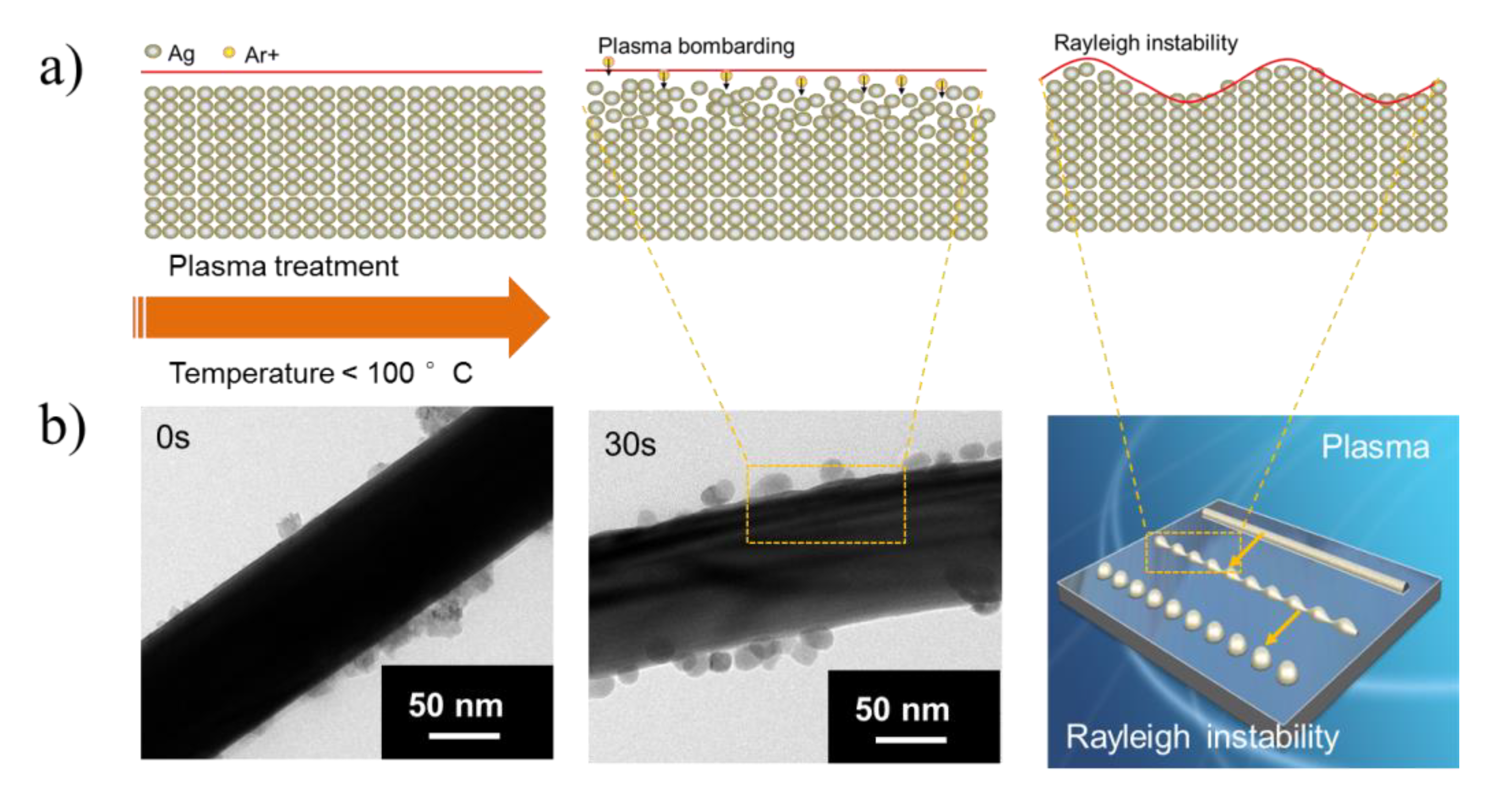
Based on the above results, RF plasma treatment shows significant differences with that of traditional thermal induced coarsening due to its low temperature need, rapid and highly ordered conversion on AgNWs. A schematic illustration has been presented to explicate the RF plasma treatment induced uniform conversion of AgNWs, as shown in
Figure 3a. When the Ar
+ plasma bombarding is exerted on AgNWs, the kinetic energy of Ar
+ is passed to the atoms on AgNWs surfaces and then to the delivered inside. Such plasma bombarding will greatly enhance the diffusing tendency of Ag atoms on AgNWs [
22]. Similar conversion of AgNWs have also been found in AgNWs networks by laser-driven and electro-temperature driven Rayleigh instability at a temperature above 360 °C [
23,
24]. Obviously, the temperature needed for RF plasma treatment is much lower. The initial surface roughness of Ag nanowire is rarely low and has little effects on the instability of the nanowires. Note that the initial surface roughness on Ag nanowire surface (0 s) observed in
Figure 3b is broken carbon film of copper mesh. TEM results show that significant surface fluctuation occurs with only 30 s plasma treatment, which proves the faster nonequilibrium diffusion of Ag atoms on AgNWs surfaces by plasma bombarding, as shown in
Figure 3b. Following this, rapid surface instability occurs on AgNWs, which leads to the conversion of AgNWs into uniform particle-chains. In this process, the diffusion is mainly localized on AgNWs surface, that’s why there is little temperature increase on the whole substrate.
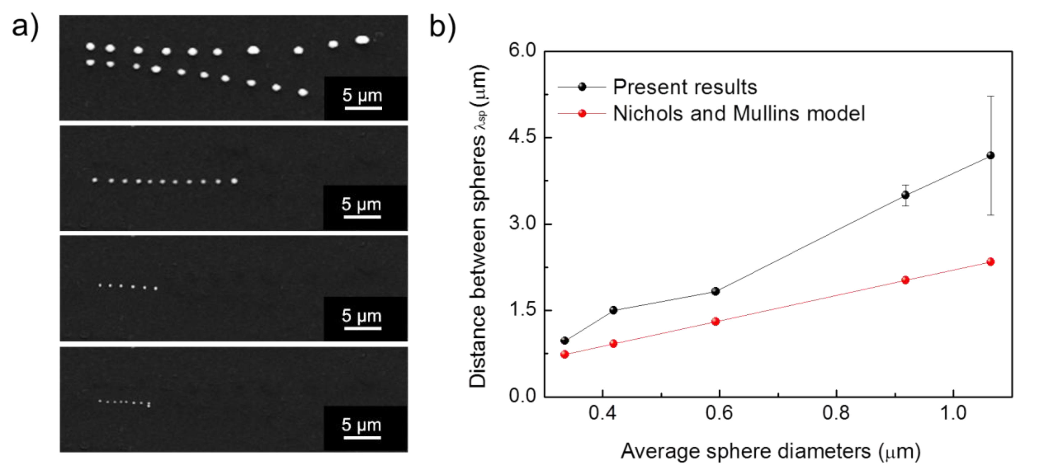
As shown in
Figure 4a, AgPCs with higher periodicity can be obtained through plasma bombarding. The statistical results of centre-to-centre distances between Ag nanoparticles (
), and the average sphere diameters of Ag nanoparticles (
) have been presented in
Figure 4b. Additionally, the diameters of Ag nanoparticles are proportional to the sphere diameters. Apparently, the
shows linear relationship with
, which well accords with the surface diffusion induced Rayleigh instability predicted by Nichols and Mullins [
25]. The deviations with Nichols-and-Mullins model can be attributed to the oblate spheroid shaped Ag nanoparticles and pentagonal shaped AgNWs which are different from the perfect cylinders and balls in the theoretical model. The standard deviations of
decrease rapidly from 24.7 % to 1.8 % as the
decreases from about 1.0 μm to 0.34 μm, which is still much smaller than that by high temperature heat treatment. As a result, the plasma treated Ag nanowires are just like isotropic materials with high diffusion abilities, which have rapid and thorough conversion properties to transform into highly ordered particle-chains at a temperature below 100 °C. Owing to this, these highly ordered particle-chains could be applied as plasmon waveguides to obtain high quality near field optical transmissions.
Obvious periodic fracture on AgPCs can be found when AgNWs are overlapped. As shown in
Figure 5a, the
at the junction area marked by yellow dotted circle are much greater than that away from this area. With the increase of the aggregation of AgNWs, insufficient coarsening on AgNWs can be observed and the periodicity of AgPCs is thoroughly broken. When AgNWs are combined into high density networks, plasma treatment can lead to uniform wire–wire welding, and will not cause fracture or coarsening on AgNWs during a short time treatment. This is probably because of the scattering and propagating of the plasma kinetic energy [
24]. It is well known that the plasma kinetic energy offers diffusion forces to Ag atoms on AgNWs surfaces in all directions within an ultra-short time, but then decrease rapidly with the distance from the AgNWs surfaces due to the scattering and propagating of kinetic energy (
Figure 5b), which means the average kinetic energy exerted on AgNWs could be significantly reduced, thereby greatly reducing the diffusion capacity of Ag atoms on AgNWs surfaces. Meanwhile, Rayleigh instability on nanowires is broken because of the changes in nanowire surface energy. When AgNWs are overlapped, the surface energy of AgNWs at the junction is changed due to the changes in their mass and curvatures on nanowires. AgNWs network with a great number of junctions in a large-scale leads to a random surface energy distribution on AgNWs, which causes the invalidation of the Rayleigh instability. In this case, Ostwald Ripening could be the main reason for the uniform wire–wire welding in AgNWs networks [
26], which prevents further fracture and coarsening on AgNWs during short time plasma treatment. Apparently, this rapid and uniform and low temperature needed wire–wire welding technology meets the urgent needs of Ag nanowire-based transparent conductive electrodes with high performances.

 ,
, 


