Article

Exploiting the Combination of Displacement and Chemical Plating for a Tailored Electroless Deposition of Palladium Films on Copper

1
Department of Chemistry “Ugo Schiff”, University of Florence, Via della Lastruccia 3, 50019 Sesto Fiorentino (FI), Italy
2
National Interuniversity Consortium of Materials Science and Technology (INSTM), Via G. Giusti 9, 50121 Firenze (FI), Italy
3
National Research Council-Organometallic Compounds Chemistry Institute (CNR-ICCOM), Via Madonna del Piano 10, 50019 Sesto Fiorentino (FI), Italy
4
Department of Engineering “Enzo Ferrari”, University of Modena and Reggio Emilia, Via Università 4, 41121 Modena (MO), Italy
5
Center for Colloid and Surface Science (CSGI), Via della Lastruccia 3, 50019 Sesto Fiorentino (FI), Italy
*
Authors to whom correspondence should be addressed.
L.F. and W.G. contributed equally to the manuscript.
Submission received: 16 July 2021 / Revised: 7 September 2021 / Accepted: 8 September 2021 / Published: 10 September 2021
(This article belongs to the Special Issue Recent Advances in Application of Coatings and Films)

Abstract

:
Various formulations for electroless deposition, to obtain continuous nanometre-sized and micrometre-sized films of palladium on copper, were compared. We deposited ultrathin films using displacement plating formulations. We obtained continuous films with an equivalent thickness between 6 and 22 nm, measured by exploiting the K-ratio method with SEM-EDS of Pd layers. The Pd films obtained in this step of the work represent a cost-effective catalytic substrate. As a second step, we selected chemical plating as the procedure to obtain palladium films with a thickness in the micrometre range. An ammonia-based Pd chemical plating bath represent one of the most effective chemical plating formulations. To prevent copper substrates from being damaged by ammonia, displacement plating with palladium was also applied as a pre-treatment to make the use of these plating baths a viable way to obtain thicker palladium coatings. Palladium films showing good adherence, compact morphology, and a thickness over 1.5 μm were obtained, proving that the combination of two different electroless techniques was the key to develop a sustainable procedure for micrometre-sized palladium coatings, which could substitute electroplating of Pd in galvanic industry for decorative applications.

1. Introduction

The importance of palladium lies in its unique ability to adsorb hydrogen and catalyse hydrogenation and dehydrogenation reactions. Palladium plays a fundamental role in a wide range of applications: in the energy field for the production [1], storage [2] and use of hydrogen in catalytic fuel cells [3,4,5], and even in the chemical synthesis field with applications in optoelectronics [6] and biology [7,8]. It is estimated that it is the element with the highest hydrogen adsorption capacity, managing to store volumes equal to 935 times its own [9]. These characteristics make this element extremely functional for the development and production of new energy systems that are not dependent on oil, such as fuel cells [2]. Nowadays, palladium is mainly used in the automotive sector in the production of catalytic converters. In 2020, China requested a 30% increase in the quantity of palladium inside cars and trucks [10]. The major problem related to the use of palladium is its high and constantly growing cost, due to the increasing need to transition from an economy based on oil to one based on hydrogen [11], and the very high demands from the automotive sector to achieve increasingly stringent environmental standards in vehicle emissions. To stem this problem and make an eco-sustainable system advantageous, even economically, it is essential to study techniques for producing thin films of palladium, to avoid the massive use of metal while preserving the surface properties that have made it so widespread.
Palladium is also particularly popular in the electroplating industry for luxury jewellery and accessories in which it is used as intermediate layer or top layer with thicknesses ranging from 0.2 μm to 1 μm [12]. In this sector, palladium films obtained from an electroless deposition could open the doors to a more cost-effective industrial process with respect to the electrodeposition one.
Electroless deposition techniques differ from electroplating due to the absence of an external current designed to promote a reduction in the species to be deposited on the substrate. In electroplating techniques, the growth of the deposit depends on the surface current density, which, for irregular geometries, is not uniformly distributed over the cathodic area, leading to non-uniform deposits. This problem does not occur with electroless depositions (given the non-use of external current) making these techniques excellent for use on substrates with exotic and irregular shapes [13].
The aim of this work is the development of a cost-effective technique or combination of techniques able to produce high-quality Pd thin films with tailorable thickness on copper substrates. To obtain a Pd layer with a very cost-effective procedure, electroless plating techniques were selected for the procedures.
Copper was chosen as the base material because it is a common material used as a substrate, as well as intermediate layer, in electroplating and the surface finishing industry thanks to its semi-noble behaviour, high levelling power, and the brightness of copper films. Unfortunately, electroless deposition of palladium on copper is not trivial and can lead to some issues. These problems are due to the presence of concentrated ammonia in most electroless palladium baths; in fact, a pre-deposition step is mandatory for Cu substrates. As proof of the fact that ammonia acts as an etchant on copper surfaces, its effect has also been studied in the literature as a copper surface polishing agent [14]. In the case of this work, ammonia etchant behaviour is detrimental for the formation of a continuous and adherent Pd layer.
In this work, two different types of electroless deposition techniques were used, displacement deposition and chemical deposition. The displacement deposition technique (PDP, palladium displacement plating, from now on) is a process in which the ions of a nobler metal, with respect to the metal substrate, are reduced on the substrate due to a galvanic exchange reaction, producing a deposited film [13].
Chemical plating is the most used electroless deposition technique [15] (PCP, palladium chemical plating, from now on) because it is more efficient than displacement plating baths allowing to obtain palladium deposition rates of over 2.5 μm/h at a deposition temperature of 50–60 °C [16]. The deposit is formed exclusively on catalytically active substrates, thanks to the reduction of metal ions in the solution by a reducing agent present in the bath. Chemical deposition is defined as a process in which one has the formation of a metal film through a controlled chemical reaction, catalysed by the same deposited metal [17]. This technique is widely used to deposit metallic films on non-metallic surfaces, e.g., glass and ceramics, through a pre-treatment to make catalytically activates the surfaces [18,19].
Unlike chemical deposition processes, displacement plating does not include an external reducing agent, it ends as soon as the noblest metal, palladium in this case, completely covers the substrate. For this reason, this technique can produce only very thin films, which is an advantage for catalytic applications but an issue for decorative applications. Chemical plating has the advantage of selectively depositing on the conductive area of a substrate, a useful feature in various areas, such as the preparation of printed circuits [20]. Electroless deposition can be found in the literature in a large number of metal/substrate combinations [21,22]; for example, metallization of semiconductor surfaces [23,24], deposition of Ag-Pd alloys [25,26], deposition of Pt on Ti surface [27], deposition of noble metals on Ge [28], Cu film formation on metal nitrides [29], Cu and Ni deposition on Al surfaces [30,31,32,33], metallization of carbon nanotubes [34], and deposition of Ag, Cu and Au surfaces [35,36]. The particular case of Pd on Cu can be found a limited number of reports [15,20,37], where authors did not study the homogeneity of the deposits over the entire substrate area nor their thickness or their adhesion and stability over time. Moreover, the combination of different electroless techniques to develop a complete process with tailorable Pd thicknesses has never been studied, to the best of our knowledge. In particular, Djokic [15] studied the influence of temperature and pH on the deposition rate of Pd-P alloys, analysing their crystalline structures. Johnson [20] studied both the aging of the plating solution and the thickness of the obtained Pd layer, but due to the date of publishing (1961) the thickness data obtained could be revised using more modern techniques. Ojani [37] studied electroless deposition of Pt-Pd alloys as catalysts for HER (hydrogen evolution reactions) reporting the composition and the surface morphology of the deposited alloys, but without paying attention to the adhesion of the obtained structures.
In this work we attempted to combine two different palladium electroless processes to deposit palladium films with tailored thicknesses on copper. To achieve this aim, selected PDP baths were tested to obtain thin palladium films. Low-thickness palladium films have the dual role of being applied as an affordable catalytic surface in the energy and automotive sectors or by protecting copper substrates from subsequent PCP baths based on ammonia, which to our knowledge are the best-performing palladium chemical plating baths available in the literature [16,20]. Ammonia-based PCP baths we used contained hypophosphite as a reducing agent for the formation of the palladium coating. This type of formulation was the best alternative to hydrazine-based PCP baths in terms of performance, although the palladium film could incorporate phosphorus forming Pd-P alloys [13,15]. Hydrazine represents the first type of reducing agent studied for the chemical deposition of different metals, such as nickel, copper [38,39,40], and also palladium [41]. Hydrazine represents a less green and safe alternative to hypophosphite due to its hazardous properties, such as its flammability and toxicity [42].

2. Materials and Methods

In this work, three different PDP solutions were tested to study the displacement of electroless deposition of palladium, both as a method to obtain nanometre-sized continuous layers and as a pre-deposition treatment applicable to PCP with the aim of producing high-quality micrometre-sized palladium layers. These three different displacement deposition solutions, from three different authors, were selected as the sole alternatives available in the literature.
All the solutions involved in this study were prepared with ultrapure water (18.2 MΩ, TOC ˂ 5 ppb) obtained with a Sartorius Arium® mini system (Göttingen, Germany). The PDP solutions were prepared using different quantities of PdCl2 salt 99.9% (Alfa Aesar, Heysham, Lancashire LA3 2XY, UK) and HCl 37% (VWR AnalaR® NORMAPUR®, Radnor, PA, USA). The PCP solutions were obtained using the same PdCl2 salt and HCl purchased before for the PDP solutions and NH3 28% (VWR AnalaR® NORMAPUR®, Radnor, PA, USA), NaH2PO2∙H2O (Carlo Erba, Cornaredo, Italy) and NH4Cl (Merck Millipore Suprapur®, Burlington, MA, USA) were added.
The composition of PDP solutions studied are reported in Table 1.
Solutions A, B, and C were developed, respectively, by Djokić [15], Johnson [20] and Pearlstein [16], and were prepared simply by adding palladium salt in a HCl solution, and then stirred until complete dissolution of the salt at room temperature.
The bath developed by Pearlstein and Weightman [16] (Table 2) was selected as the PCP solution used in this work due to its efficiency and its stability over time and work cycles.
To obtain the best performances in terms of Pd film quality and bath stability, the PCP solution (presented in Table 2) preparation was meticulously carried out. The Pd solution was prepared by dissolving 0.1 g of PdCl2 in a flask containing 0.2 mL of 37% HCl. Within the flask, palladium was present in the form of [PdCl4]2. To the previously prepared solution, 8 mL of 28% NH3 was added little by little under stirring, forming a light-pink precipitate. The flask was closed and left under stirring for an hour until the solution became transparent. It was then left to mature for a total of 24 h. Transparency indicated the formation of the chelate [Pd(NH3)4]2+. The contents of the flask were subsequently filtered into a 25 mL flask with a syringe and a glass fibre filter to remove any pollutants that could lead to the deterioration of the solution. In parallel to this, a solution of sodium hypophosphite monohydrate was made by dissolving 0.5 g in 25 mL of ultrapure water. Finally, the two solutions were combined in a 50 mL flask.
The copper substrates (pure copper, dimensions 50 mm × 10 mm × 1 mm) used in the entire work were pre-treated using different steps. Pre-treatment of the copper substrates was an irreplaceable step due to the copper oxide layer that naturally formed over the entire surface, which passivated it, blocking the galvanic exchange reaction between copper atoms and palladium ions, which produced the electroless deposited film.
First, the metallic slabs were polished with a polishing machine using a soft polishing brush and polishing wax. Then, to completely remove the organic residues due to the polishing wax, it was necessary to stir the copper plates inside toluene for about 3 min and the rinse with abundant ultrapure water. Each copper plate was masked with the help of Teflon tape to obtain a reproducible deposition area (approximately 1 cm × 1 cm on the bottom of the plate) and further degreasing with acetone was performed. In a second step, an electrochemical cathodic degreasing was then carried out using copper as a cathode and a mixed oxide counter electrode inside a commercially available alkaline degreasing solution (DEXO 102, Italfimet, Arezzo, Italy). Copper plates were then, rinsed with ultrapure water, dipped in a neutralization solution (H2SO4 0.5 M), and rinsed again with ultrapure water. The cathodic degreasing acts as a pre-treatment for the copper surface as it removes copper oxide through H2 bubbling and the organic residues using the soap in the solution. All the Pd depositions were performed at 20 °C (except where differently stated). Both the beaker and the stir bar (when used) were carefully cleaned with a piranha solution and aqua regia after each single use.
A scanning electron microscopy coupled with energy dispersive X-ray spectroscopy detector (SEM-EDS) analysis was performed with a Hitachi S2300 (Tokyo, Japan) using an acceleration voltage of 20 keV, equipped with a Thermo-Fisher Scientific Noran System 7 detector (Waltham, MA, USA) and analysed with Pathfinder 1.3 software.
Equivalent metal film thickness determination with EDS spectra was made possible by applying the K-ratio method [43,44]. Selecting a particular X-ray emission signal of an element (in this case Kα for copper and Lα for palladium) in the EDS spectra, the ratio between the area of this signal derived from the metal layer with a specific thickness and the one derived from the bulk metal is called the K-ratio. In this case NIST DTSA-II software [45] was used to simulate the EDS spectra of different palladium films with known thicknesses using a Monte Carlo approach [43,44], applying the work parameters of the Hitachi SEM used for the real samples. The calibration curve obtained from the simulated K-ratios vs. standard metal film thickness was used to interpolate the K-ratio values obtained from real palladium films with unknown thicknesses. The thickness values calculated using this method are “equivalent thicknesses” obtained by interpolating a regression curve.
Optical microscopy analysis (OM) was carried out with a Nikon Eclipse L 150 (Tokyo, Japan) with the image acquisition software NIS-Elements F 2.20.
X-ray fluorescence spectroscopy (XRF) of palladium films on copper was carried out using a Bowman BA-100 (Schaumburg, IL, USA), previously calibrated with Bowman certified palladium standard (0.99 µm) on bulk copper.

3. Results

Extensive bibliographic research and preliminary deposition tests were performed to verify the performances of deposition for both PDP and PCP solutions. Then, the three PDP solutions presented in the previous section were selected for tests, which of allowed to obtain the best performances in terms of film thickness and morphology. Each solution was tested combining different deposition times and the presence or the absence of stirring. The list of performed tests is reported in Table 3.
The deposition parameters selected to produce samples #1 to #12 were chosen to compare the performances of the PDP solution in the presence and absence of stirring, combining two deposition times. Shorter deposition times with respect to those already studied in the literature (12 min in the case of Johnson’s work [20]) were selected in order to study the possibility of obtaining an ultrathin but continuous palladium layer, to achieve sustainability in terms of precious metal amount, which is the one of the main aims of this work.
Once the deposition was completed (Figure 1), the thus obtained plates were rinsed abundantly with ultrapure water and dried under a nitrogen flow. To address the film quality and thickness, the obtained deposits were analysed using various techniques, such as OM, SEM-EDS and XRF.

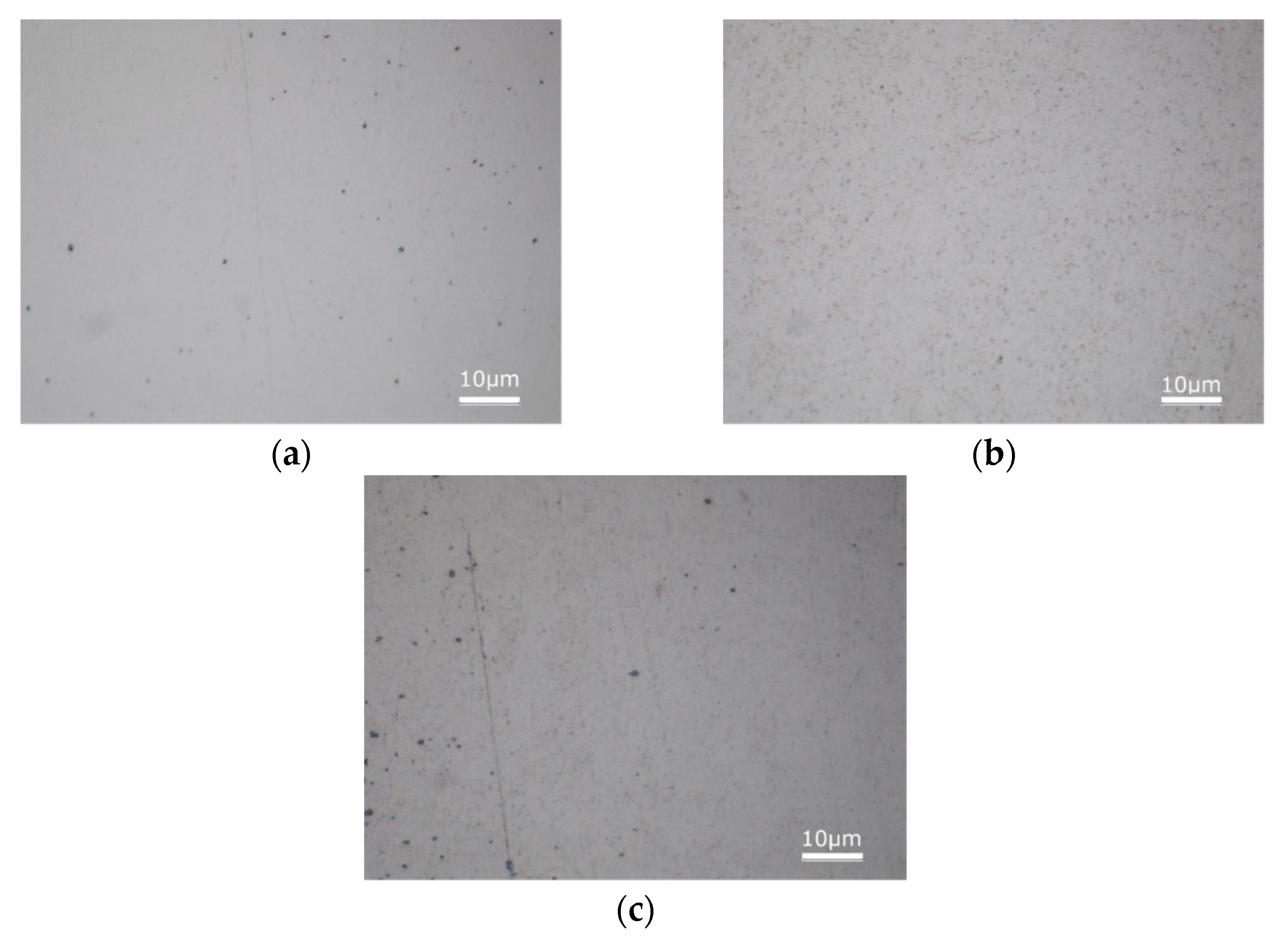
3.1. Palladium Displacement Plating Characterization

Due to the very low amount of palladium deposited with the PDP method, SEM-EDS analysis was used to measure the film thickness. The EDS spectra of the specimens made of copper with various thicknesses of palladium were simulated using NIST DTSA-II software. From the spectra, the K-ratio was calculated to build a calibration curve (Figure 2) [43,44]. K-ratios were defined as the ratio between the peak intensity (X-ray counts) for the element of interest in the sample and the peak intensity of the pure element at the same energy. Then, the spectra of our real samples were recorded, the K-ratio was calculated and the thickness was obtained by means of the calibration curve.
The calibration curve for the thickness determination was built simulating the following thicknesses of palladium on copper: 0 nm, 5 nm, 10 nm, 20 nm, 50 nm, and 75 nm (Figure 2 inset). The simulated points are not equally spaced because the correlation between thickness and K-ratio is exponential; in this way, the fitting is more reliable and optimized, keeping the number of points low. For low metal thicknesses, the correlation between the K-ratio and the thickness values can be approximated by a second-grade equation which provides a simpler regression maintaining a high reliability (R2 > 0.999).
The thicknesses obtained with the K-ratios through the calibration curve are reported in Table 4. The standard deviation was calculated from the values provided by the EDS spectra.
From the results obtained, comparing the same deposition solution, an increase in deposition time seemed to act in a more relevant way than the presence or the absence of stirring did on the obtained thickness. Although the presence of stirring also contributed to increasing the Pd thickness, guaranteeing a constant concentration of Pd ions at the substrate–solution interface. EDS analysis did not detect the presence of Pd in sample #3. For this reason, in Table 4, the K-ratio and the thickness values are 0.
OM was used to verify the absence or presence of discontinuities and defects due to an incomplete coverage of the copper substrate. Samples #6, #8, and, #10 were observed using optical microscopy. These three samples were selected because they were the best results obtained from each deposition solution (A, B, and C) in terms of macroscopical homogeneity and palladium thicknesses measured using the K-ratio method. OM images of samples #6, #8, and #10 are reported in Figure 3.
Comparing the three different samples from an optical microscopy point of view, the surfaces resulted in being sufficiently homogeneous and compact, as could be seen by observing the samples with the naked eye. The presence of small bumps and scratches (Figure 3) was attributed to the imperfections present on the copper substrate and not to the palladium deposition. Sample #6 represented the best result obtained using PDP bath B, described by Johnson [20]; in the present work, the same composition and the best conditions discovered by Johnson during his work were used (25 °C, 250 mL/L HCl 32% = 216 mL/L HCl 37%, Pd 5 g/L) except for deposition time, which was 12 min for Johnson and 90 s in the present work. Johnson obtained shiny Pd films of 70 μin (1.778 μm) without exfoliations (average deposition rate = 148 nm/min). In the present work, we obtained a Pd deposit of 22.2 nm in 90 s (average deposition rate = 14.8 nm/min). The discrepancy between the two deposition rates could be explained by considering the autocatalytic effect that Pd film has towards its deposition, which could change the rates during the early minutes of deposition.
Sample #8 was the best result obtained by the authors for PDP solution A, developed by Djokic [15], but could not be compared with the results obtained by that author because he used the PDP bath only as a surface pre-treatment without paying attention to the results derived from the displacement plating and the thickness of the film formed.
Sample #10 was obtained from PDP solution C, used by Pearlstein and Weightman [16] and represents the sample with a minor amount of palladium deposited besides the three best samples selected in the present work due to the low concentration of metal precursor in the solution. Pearlstein used this PDP solution as a pre-treatment of the metal substrate without studying this treatment in depth, as in the case of Djokic, a comparison with the results obtained in the present work is not possible.
Sample #12, although showing a much higher palladium thickness than sample #6 (both obtained from deposition solution B), after 7 days, showed a wide exfoliation of the palladium film that we attributed to the poor adhesion of the film derived from the excess of residual internal stress [46]. During formation, thin films can develop large intrinsic stresses [47,48]. These stresses can have a magnitude that exceed that of the same bulk material. The residual internal stresses developed by thin films relax forming blisters or exfoliations (as in the case of PDP sample #12, Figure 4) at different time scales, which ranges from hours to days. For this reason, the authors selected 7 days as an acceptable time scale for monitoring the eventual relaxation of stresses developed by Pd films during deposition.

3.2. Palladium Chemical Plating Characterization

To obtain an adherent deposited layer, is not sufficient that the copper substrate be cleaned, it should also be not damaged by the PCP. The same PDP procedures employed for samples #6, #8, and #10, were used as pre-deposition for PCP (obtaining samples #6C, #8C and #10C, respectively) to evaluate which one was the most protective one towards Cu base material, since copper is severely attacked by the high concentration of ammonia present in the PCP solution. In addition, the effectiveness of the PCP is valuable for application in which deposits in the micron range are requested. Each PDP pre-deposition was carried out immediately before PCP. The PCP depositions were performed without stirring at a temperature of 55 °C and for a duration of 60 min. In Figure 5, it is possible to observe the samples 7 days after the deposition. The copper substrate, which was not covered with a protective PDP, although it was not immersed in the solution, was strongly corroded by the ammonia vapours. In the bottom part of the samples, where the pre-deposition was carried out, a homogeneous and shiny palladium deposit is visible. After one week, sample #6C underwent a strong exfoliation, while the other two samples appeared intact to the naked eye. As can be seen from Figure 5, PCP sample #6C showed the copper substrate under the palladium exfoliation. Our hypothesis on the failure of this sample regards the poor stability of the PDP pre-deposition performed on this sample. As already observed for PDP sample #12, the relaxation of residual internal stresses developed by Pd thin film on copper was the origin of the detachment of the PDP+PCP palladium coating on sample #6C, and occurred in a time range longer than the 7 days during which the PDP pre-depositions were monitored.
The deposits obtained were analysed using XRF [49,50], the total palladium film thicknesses obtained summing PDP+PCP processes are shown in Table 5. The average values and the standard deviations were the result of three measurements carried out in different spots that were randomly chosen.
In Figure 6 it is possible to appreciate the deposits analysed using OM, 7 days later in the deposition process. Deposit #10C was the most homogeneous, free of defects and even the thickest, while sample #6C presented extended exfoliations which brought to light the characteristic colour of the copper substrate; sample #8 showed cracks.
Sample #10C, obtained by the combined process of PDP + PCP applying the PDP and PCP solutions already exploited by Pearlstein and Weightman [16] was the best result in terms of Pd film adhesion, homogeneity, and absence of surface defects (cracks, blisters or exfoliations). In the work of Pearlstein and Weightman, the authors stated a deposition rate of over 2.5 μm/h for the PCP on copper. In the present work, applying the same conditions of the aforementioned work, the authors obtained a growth of 1.78 μm of Pd in 1 h. The discrepancy between the two values can be due to two main factors. In Pearlstein’s work, the PDP pre-treatment was longer and another pre-treatment based on a tin electroless bath was anticipated, which altered the catalytic activity of the surface on the oxidation of hypophosphite in the PCP bath. Second, the thickness determination method used in the present work for the PDP+PCP samples (X-ray spectroscopy) was more accurate than the gravimetric method applied by Pearlstein and co-worker.

4. Conclusions

In conclusion, two different but combinable types of electroless deposition techniques were tested to obtain palladium films without cracks, exfoliations, or blisters on copper substrates. Applying palladium displacement deposition, we obtained very thin metal films with equivalent thicknesses ranging from 6.1 to 22.2 nm, measured with a SEM-EDS K-ratio method. Moreover, the possibility to plate only the metallic surface of the substrate, which is the main feature of electroless plating based on galvanic displacement, represents an interesting option in fuel cell electrodes fabrication with novel geometries in which palladium surface contours must be finely tuned.
Palladium films obtained by displacement plating on copper were used as protective undercoat to perform palladium chemical plating from an ammonia-based bath, which otherwise could not be applied due the corrosive behaviour of ammonia for copper substrates. A high-quality palladium film with thickness of 1.78 μm (sample #10C) were obtained applying the combined procedure we studied using the Pearlstein and Weightman pre-deposition (solution C). This result is proof of the integrity of the palladium coating obtained by displacement plating represents a valuable alternative for applications where thick palladium films on copper are requested. The combination of PDP + PCP studied in the present work could represent a valuable alternative to palladium electroplating in jewellery and luxury good industries, where this metal is widespread as an intermediate layer or topcoat. Palladium electroless plating is a valid alternative to electroplating thanks to the lower investment required for industrial plants and the electricity savings required for the process.
Future developments will regard the refinement of the control of Pd thickness both in single and in combined techniques mode. Moreover, Pd film needs to be characterized more in depth from the mechanical and compositional point of view based of specific areas of application to which it will be applied.

Author Contributions

Conceptualization, W.G. and L.F.; methodology, W.G. and L.F.; software, W.G.; validation, F.V. and M.I.; formal analysis, W.G., L.F. and F.B.; investigation, W.G., L.F. and F.B.; resources, F.V. and M.I.; data curation, W.G., L.F. and F.B.; writing—original draft preparation, L.F.; writing—review and editing, W.G., M.B., H.M., C.F. and F.V.; supervision, M.I. and W.G.; project administration, F.V. and M.I.; funding acquisition, F.V. and M.I. All authors have read and agreed to the published version of the manuscript.

Funding

This research was funded by Ministero dell’Istruzione, dell’Università e della Ricerca (PRIN “Progetti di Ricerca di Rilevante Interesse Nazionale”, which made possible the project “Novel Multilayered and Micro-Machined Electrode Nano-Architectures for Electrocatalytic Applications (Fuel Cells and Electrolyzers)”), grant number 2017YH9MRK.

Data Availability Statement

The data presented in this study are available in the body of the text.

Acknowledgments

PRIN “Progetti di Ricerca di Rilevante Interesse Nazionale” is acknowledged for the financial support.

Conflicts of Interest

The authors declare no conflict of interest. The funder had no role in the design of the study; in the collection, analyses, or interpretation of data; in the writing of the manuscript, or in the decision to publish the results.

References

  1. Patel, N.; Patton, B.; Zanchetta, C.; Fernandes, R.; Guella, G.; Kale, A.; Miotello, A. Pd-C powder and thin film catalysts for hydrogen production by hydrolysis of sodium borohydride. Int. J. Hydrogen Energy 2008, 33, 287–292. [Google Scholar] [CrossRef]
  2. Adams, B.D.; Chen, A. The role of palladium in a hydrogen economy. Mater. Today 2011, 14, 282–289. [Google Scholar] [CrossRef]
  3. Bambagioni, V.; Bianchini, C.; Marchionni, A.; Filippi, J.; Vizza, F.; Teddy, J.; Serp, P.; Zhiani, M. Pd and Pt–Ru anode electrocatalysts supported on multi-walled carbon nanotubes and their use in passive and active direct alcohol fuel cells with an anion-exchange membrane (alcohol=methanol, ethanol, glycerol). J. Power Sources 2009, 190, 241–251. [Google Scholar] [CrossRef]
  4. Miller, H.A.; Lavacchi, A.; Vizza, F.; Marelli, M.; Di Benedetto, F.; D’Acapito, F.; Paska, Y.; Page, M.; Dekel, D.R. A Pd/C-CeO 2 anode catalyst for high-performance platinum-free anion exchange membrane fuel cells. Angew. Chem. Int. Ed. 2016, 55, 6004–6007. [Google Scholar] [CrossRef] [PubMed]
  5. Calderón Gómez, J.; Moliner, R.; Lázaro, M. Palladium-based catalysts as electrodes for direct methanol fuel cells: A last ten years review. Catalysts 2016, 6, 130. [Google Scholar] [CrossRef] [Green Version]
  6. Tsuda, T.; Choi, S.-M.; Shintani, R. Palladium-catalyzed synthesis of dibenzosilepin derivatives via 1, n -Palladium migration coupled with anti -Carbopalladation of alkyne. J. Am. Chem. Soc. 2021, 143, 1641–1650. [Google Scholar] [CrossRef]
  7. Du, S.; Wang, W.-F.; Song, Y.; Chen, Z.; Wu, X.-F. Palladium-catalyzed cascade carbonylative synthesis of 1,2,4-triazol-3-ones from hydrazonoyl chlorides and NaN3. Org. Lett. 2021, 23, 974–978. [Google Scholar] [CrossRef]
  8. Kitamura, Y.; Murata, Y.; Iwai, M.; Matsumura, M.; Yasuike, S. Palladium-catalyzed C–H arylation of benzofurans with triarylantimony difluorides for the synthesis of 2-arylbenzofurans. Molecules 2020, 26, 97. [Google Scholar] [CrossRef]
  9. Greenwood, N.N.; Earnshaw, A. Chemistry of the Elements, 1st ed.; Elviser: Amsterdam, The Netherlands, 1984; pp. 268–327. [Google Scholar]
  10. Hobson, P. ‘There’s No Metal’: Record-Breaking Palladium Races Higher. Reuters. 2020. Available online: https://www.reuters.com/article/us-palladium-price-graphic-idUSKBN1ZG1T6/ (accessed on 9 September 2021).
  11. Vigne, S.A.; Lucey, B.M.; O’Connor, F.A.; Yarovaya, L. The financial economics of white precious metals—A survey. Int. Rev. Financ. Anal. 2017, 52, 292–308. [Google Scholar] [CrossRef] [Green Version]
  12. Giurlani, W.; Zangari, G.; Gambinossi, F.; Passaponti, M.; Salvietti, E.; Di Benedetto, F.; Caporali, S.; Innocenti, M. Electroplating for decorative applications: Recent trends in research and development. Coatings 2018, 8, 260. [Google Scholar] [CrossRef] [Green Version]
  13. Djokić, S.S. Electroless deposition of metals and alloys. In Modern Aspects of Electrochemistry; Conway, B.E., White, R.E., Eds.; Springer: Boston, MA, USA, 2002; pp. 51–133. ISBN 978-0306476044. [Google Scholar]
  14. Luo, Q.; Mackay, R.A.; Babu, S.V. Copper dissolution in aqueous ammonia-containing media during chemical mechanical polishing. Chem. Mater. 1997, 9, 2101–2106. [Google Scholar] [CrossRef]
  15. Djokić, S.S. Electroless deposition of palladium using hypophosphite as a reducing agent. Plat. Surf. Finish. 1999, 86, 104–107. [Google Scholar]
  16. Pearlstein, F.; Weightman, R. Electroless Deposition of Palladium Alloys. U.S. Patent 3,754,939, 28 August 1973. [Google Scholar]
  17. Mallory, G.O.; Hajdu, J.B. Electroless Plating, 1st ed.; Elsevier: Amsterdam, The Netherlands, 1990; ISBN 978-0815512776. [Google Scholar]
  18. Fujinami, T.; Watanabe, J.; Honma, H. Catalytic activity and stability of mixed PdCl2/SnCl2 catalysts. Trans. Inst. Met. Finish. 1996, 74, 193–197. [Google Scholar] [CrossRef]
  19. Hamaya, T.; Kumagai, Y.; Koshizaki, N.; Kanbe, T. Electroless plating through successive pretreatment with aminosilane and PdCl 2. Chem. Lett. 1989, 18, 1461–1464. [Google Scholar] [CrossRef]
  20. Johnson, R.W. Immersion plating of the platinum group metals. J. Electrochem. Soc. 1961, 108, 632. [Google Scholar] [CrossRef]
  21. Paunovic, M. Electroless deposition of metals and alloys. In Electrochemistry in Transition; Springer: Boston, MA, USA, 1992; pp. 479–497. [Google Scholar] [CrossRef]
  22. Ohno, I. Electroless deposition of alloys. Mod. Electroplat. 2011, 499–506. [Google Scholar] [CrossRef]
  23. Magagnin, L.; Maboudian, R.; Carraro, C. Gold deposition by galvanic displacement on semiconductor surfaces: Effect of substrate on adhesion. J. Phys. Chem. B 2002, 106, 401–407. [Google Scholar] [CrossRef]
  24. Carraro, C.; Maboudian, R.; Magagnin, L. Metallization and nanostructuring of semiconductor surfaces by galvanic displacement processes. Surf. Sci. Rep. 2007, 62, 499–525. [Google Scholar] [CrossRef]
  25. Chen, L.; Liu, Y. Synthesis and characterization of dendritic and porous Ag–Pd alloy nanostructures. J. Colloid Interface Sci. 2011, 364, 100–106. [Google Scholar] [CrossRef]
  26. Wang, D.; Li, T.; Liu, Y.; Huang, J.; You, T. Large-scale and template-free growth of free-standing single-crystalline dendritic Ag/Pd alloy nanostructure arrays. Cryst. Growth Des. 2009, 9, 4351–4355. [Google Scholar] [CrossRef]
  27. Kokkinidis, G.; Papoutsis, A.; Stoychev, D.; Milchev, A. Electroless deposition of Pt on Ti—catalytic activity for the hydrogen evolution reaction. J. Electroanal. Chem. 2000, 486, 48–55. [Google Scholar] [CrossRef]
  28. Porter, L.A.; Choi, H.C.; Ribbe, A.E.; Buriak, J.M. Controlled electroless deposition of noble metal nanoparticle films on germanium surfaces. Nano Lett. 2002, 2, 1067–1071. [Google Scholar] [CrossRef] [Green Version]
  29. Wang, Z.; Ida, T.; Sakaue, H.; Shingubara, S.; Takahagi, T. Electroless plating of copper on metal-nitride diffusion barriers initiated by displacement plating. Electrochem. Solid-State Lett. 2003, 6, C38. [Google Scholar] [CrossRef]
  30. Djokić, S.S. Cementation of copper on aluminum in alkaline solutions. J. Electrochem. Soc. 1996, 143, 1300–1305. [Google Scholar] [CrossRef]
  31. Hutt, D.A.; Liu, C.; Conway, P.P.; Whalley, D.C.; Mannan, S.H. Electroless nickel bumping of aluminum bondpads. I. Surface pretreatment and activation. IEEE Trans. Compon. Packag. Technol. 2002, 25, 87–97. [Google Scholar] [CrossRef]
  32. Hutt, D.A.; Liu, C.; Conway, P.P.; Whalley, D.C.; Mannan, S.H. Electroless nickel bumping of aluminum bondpads. II. Electroless nickel plating. IEEE Trans. Compon. Packag. Technol. 2002, 25, 98–105. [Google Scholar] [CrossRef]
  33. Watanabe, H.; Honma, H. Fabrication of nickel microbump on aluminium substrate using electroless nickel plating. Trans. IMF 1996, 74, 138–141. [Google Scholar] [CrossRef]
  34. Qu, L.; Dai, L.; Osawa, E. Shape/size-controlled syntheses of metal nanoparticles for site-selective modification of carbon nanotubes. J. Am. Chem. Soc. 2006, 128, 5523–5532. [Google Scholar] [CrossRef] [PubMed]
  35. Mabbott, S.; Larmour, I.A.; Vishnyakov, V.; Xu, Y.; Graham, D.; Goodacre, R. The optimisation of facile substrates for surface enhanced Raman scattering through galvanic replacement of silver onto copper. Analyst 2012, 137, 2791. [Google Scholar] [CrossRef]
  36. Liu, Y.-C.; Yang, S.-J. Improved surface-enhanced Raman scattering based on Ag–Au bimetals prepared by galvanic replacement reactions. Electrochim. Acta 2007, 52, 1925–1931. [Google Scholar] [CrossRef]
  37. Ojani, R.; Raoof, J.B.; Hasheminejad, E. One-step electroless deposition of Pd/Pt bimetallic microstructures by galvanic replacement on copper substrate and investigation of its performance for the hydrogen evolution reaction. Int. J. Hydrogen Energy 2013, 38, 92–99. [Google Scholar] [CrossRef]
  38. Nobari, N.; Behboudnia, M.; Maleki, R. Palladium-free electroless deposition of pure copper film on glass substrate using hydrazine as reducing agent. Appl. Surf. Sci. 2016, 385, 9–17. [Google Scholar] [CrossRef]
  39. Kim, K.H.; Lim, T.; Park, K.J.; Koo, H.C.; Kim, M.J.; Kim, J.J. Investigation of Cu growth phenomena on Ru substrate during electroless deposition using hydrazine as a reducing agent. Electrochim. Acta 2015, 151, 249–255. [Google Scholar] [CrossRef]
  40. Bulasara, V.K.; Thakuria, H.; Uppaluri, R.; Purkait, M.K. Nickel-ceramic composite membranes: Optimization of hydrazine based electroless plating process parameters. Desalination 2011, 275, 243–251. [Google Scholar] [CrossRef]
  41. Muench, F.; Oezaslan, M.; Svoboda, I.; Ensinger, W. Electroless plating of ultrathin palladium films: Self-initiated deposition and application in microreactor fabrication. Mater. Res. Express 2015, 2, 105010. [Google Scholar] [CrossRef]
  42. Niemeier, J.K.; Kjell, D.P. Hydrazine and aqueous hydrazine solutions: Evaluating safety in chemical processes. Org. Process. Res. Dev. 2013, 17, 1580–1590. [Google Scholar] [CrossRef]
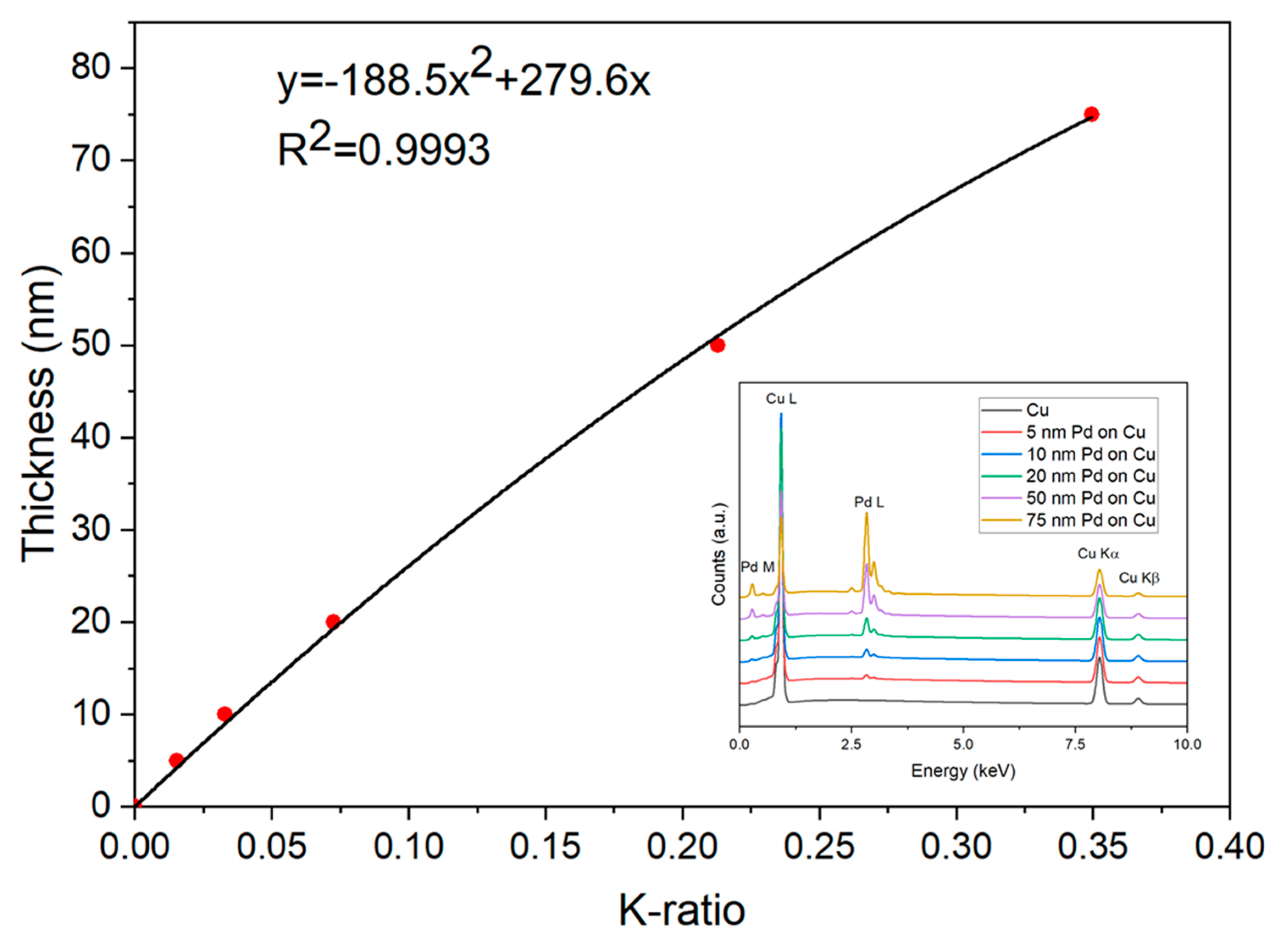
  43. Giurlani, W.; Berretti, E.; Innocenti, M.; Lavacchi, A.; Ugo, C. Measuring the thickness of metal coatings: A review of the methods. Coatings 2020, 10, 1211. [Google Scholar] [CrossRef]
  44. Giurlani, W.; Innocenti, M.; Lavacchi, A. X-ray Microanalysis of precious metal thin films: Thickness and composition determination. Coatings 2018, 8, 84. [Google Scholar] [CrossRef] [Green Version]
  45. NIST DTSA-II Software. Available online: http://www.cstl.nist.gov/div837/837.02/epq/dtsa2/ (accessed on 9 September 2021).
  46. Abadias, G.; Chason, E.; Keckes, J.; Sebastiani, M.; Thompson, G.B.; Barthel, E.; Doll, G.L.; Murray, C.E.; Stoessel, C.H.; Martinu, L. Review Article: Stress in thin films and coatings: Current status, challenges, and prospects. J. Vac. Sci. Technol. A Vac. Surf. Films 2018, 36, 020801. [Google Scholar] [CrossRef] [Green Version]
  47. Engwall, A.M.; Rao, Z.; Chason, E. Origins of residual stress in thin films: Interaction between microstructure and growth kinetics. Mater. Des. 2016, 110, 616–623. [Google Scholar] [CrossRef] [Green Version]
  48. Chason, E.; Engwall, A.; Pei, F.; Lafouresse, M.; Bertocci, U.; Stafford, G.; Murphy, J.A.; Lenihan, C.; Buckley, D.N. Understanding residual stress in electrodeposited Cu thin films. J. Electrochem. Soc. 2013, 160, D3285–D3289. [Google Scholar] [CrossRef]
  49. Giurlani, W.; Berretti, E.; Lavacchi, A.; Innocenti, M. Thickness determination of metal multilayers by ED-XRF multivariate analysis using Monte Carlo simulated standards. Anal. Chim. Acta 2020, 1130, 72–79. [Google Scholar] [CrossRef] [PubMed]
  50. Giurlani, W.; Berretti, E.; Innocenti, M.; Lavacchi, A. Coating thickness determination using X-ray fluorescence spectroscopy: Monte Carlo simulations as an alternative to the use of standards. Coatings 2019, 9, 79. [Google Scholar] [CrossRef] [Green Version]
Figure 1. Aesthetic appearance of palladium films obtained by displacement plating. Sample numbers are reported on the uncoated part of each sample.
Applsci 11 08403 g001
Figure 2. Fitting curve of simulated standard palladium film thicknesses and relative K-ratio. The fitting equation and the R2 value of the fitting equation are reported in the figure. The inset shows the simulated spectra used to obtain the K-ratios.
Applsci 11 08403 g002
Figure 3. Optical microscopy images of samples (a) #6; (b) #8, and (c) #10 after palladium displacement deposition.
Applsci 11 08403 g003
Figure 4. Exfoliation occurred on sample #12 observed by SEM in backscattered electrons mode.
Applsci 11 08403 g004
Figure 5. Palladium chemical plating samples after 7 days of aging. Sample number is reported on the uncoated part of each sample (from left to right, samples #6C, #8C, #10C).
Applsci 11 08403 g005
Figure 6. OM images of sample (a) #6C; (b) #8C and (c) #10C are shown in the figures. For samples #6C and #8C the presence of cracks can be observed (e.g., the features highlighted by the red circles) while for sample #10C the surface results were smooth and free of defects.
Applsci 11 08403 g006
Table 1. Palladium displacement plating baths nomenclature and their relative composition.
BathPdCl2 (as Pd)HCl (37%)
mMg∙L−1MmL∙L−1
A9.41.660.650
B28.252.6216
C0.560.10.0060.5
Table 2. Palladium chemical plating bath composition and conditions.
ReagentConcentration
PdCl22 g∙L1
HCl (37%)4 mL∙L1
NH3 (28%)160 mL∙L1
NaH2PO2∙H2O10 g∙L1
NH4Cl27 g∙L1
Temperature55 °C
Deposition time60 min.
Table 3. Deposition conditions for PDP samples obtained from baths A, B and C.
SamplePDP SolutionStirringDeposition Time (s)
#1ANo30
#2ANo90
#3CNo30
#4CNo90
#5BNo30
#6BNo90
#7AYes30
#8AYes90
#9CYes30
#10CYes90
#11BYes30
#12BYes90
Table 4. Equivalent thickness results obtained by EDS spectra of palladium displacement plating samples.
SampleK-RatioEDS Thickness (nm)Std. Dev. (±nm)
#10.0061.70.3
#20.0154.20.3
#30.0000/
#40.0030.80.3
#50.03910.60.3
#60.08422.20.2
#70.0102.80.3
#80.0349.30.3
#90.0041.10.3
#100.0226.10.3
#110.07018.60.2
#120.16841.70.4
Table 5. XRF thickness determination of palladium coatings. The thicknesses of the palladium coatings derived from PDP+PCP procedure are reported in the second column.
SampleAverage Thickness (μm)Std. Dev. (±μm)
#6C1.590.16
#8C1.690.18
#10C1.780.06
Publisher’s Note: MDPI stays neutral with regard to jurisdictional claims in published maps and institutional affiliations.

