
Effect of Substrate Misorientation on the Structural and Optical Characteristics of In-Rich InGaAs/GaAsP Quantum Wells

Abstract
:1. Introduction
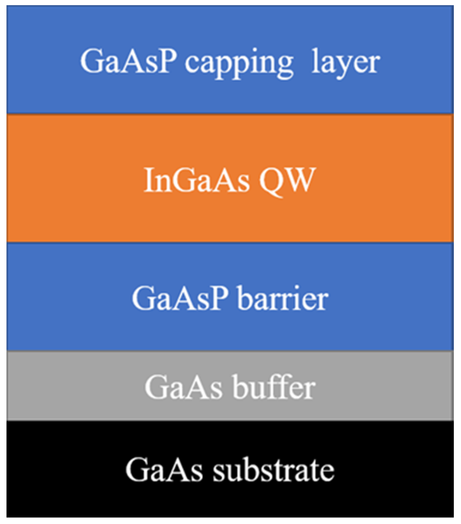
2. Materials and Methods
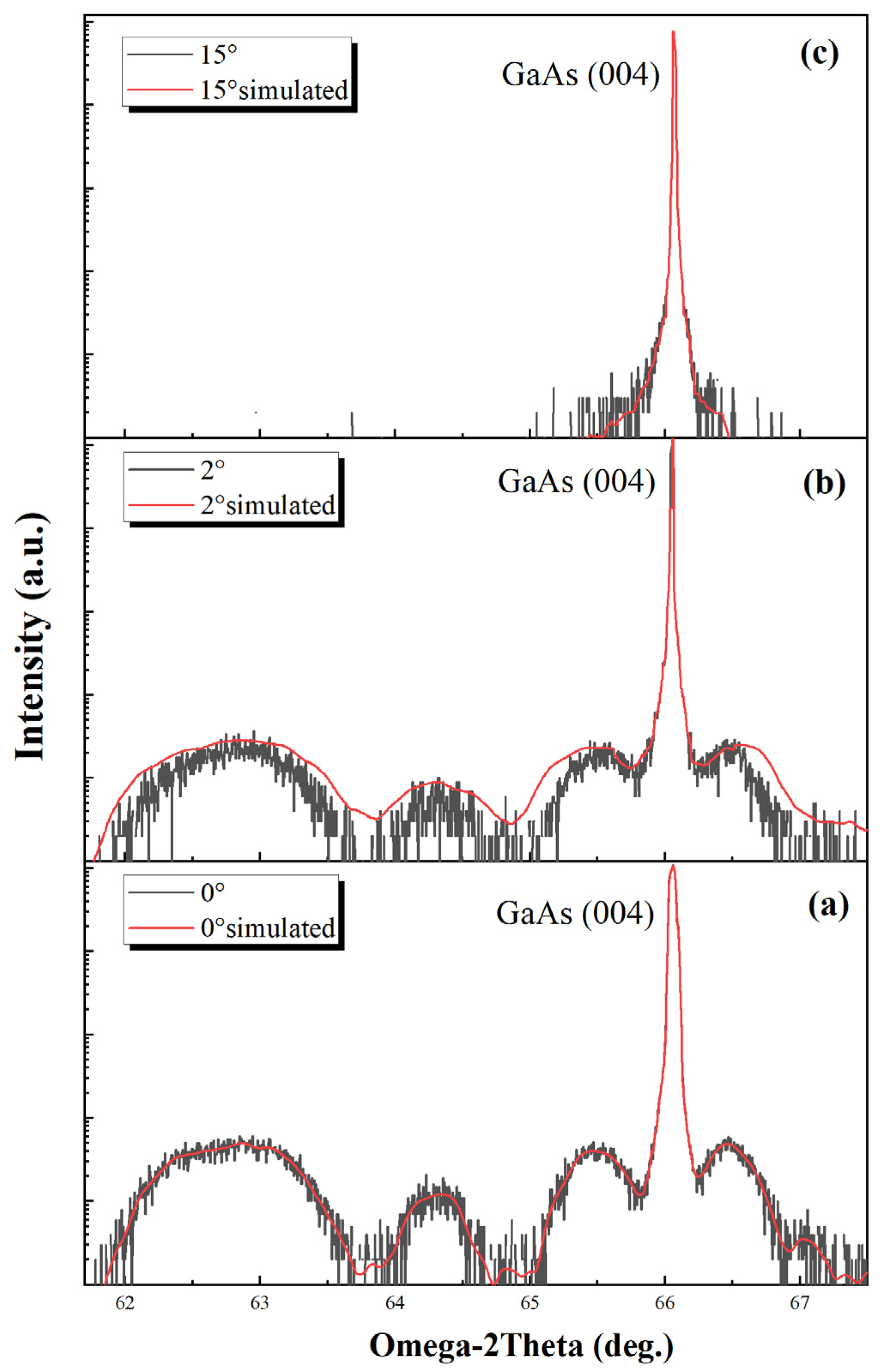
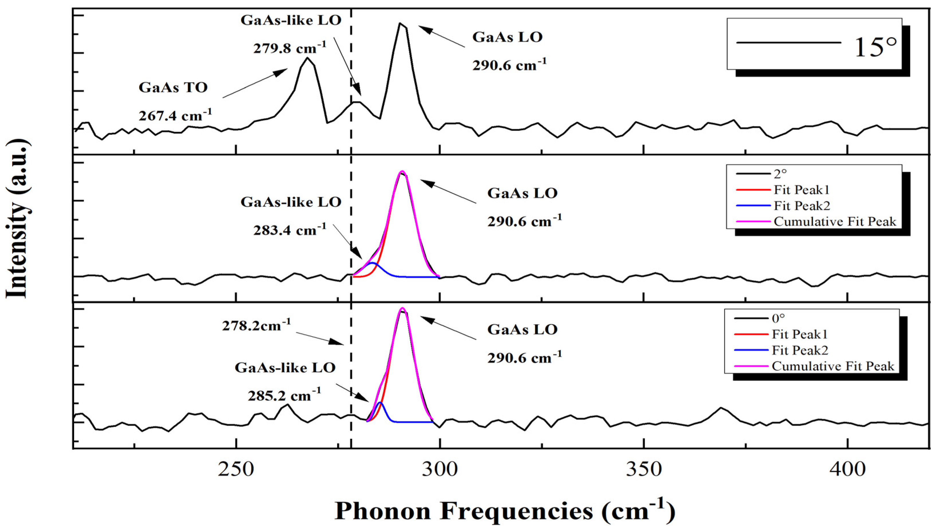
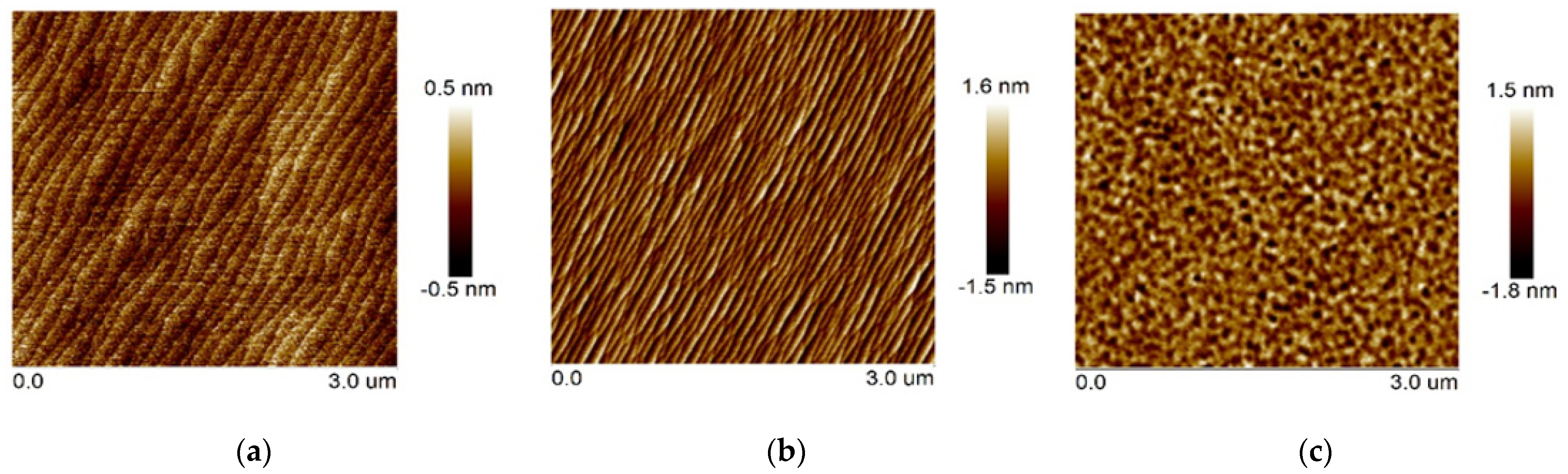
3. Results and Discussion
4. Conclusions
Author Contributions
Funding
Institutional Review Board Statement
Informed Consent Statement
Data Availability Statement
Conflicts of Interest
References
- Hou, C.-C.; Chen, H.-M.; Zhang, J.-C.; Zhuo, N.; Huang, Y.-Q.; Hogg, R.-A.; Childs, D.T.D.; Ning, J.-Q.; Wang, Z.-G.; Liu, F.-Q.; et al. Near-infrared and mid-infrared semiconductor broadband light emitters. Light-Sci. Appl. 2018, 7, 7. [Google Scholar] [CrossRef] [PubMed]
- Nagle, J.; Landesman, J.P.; Larive, M.; Mottet, C.; Bois, P. Indium surface segregation in strained GaInAs quantum wells grown on GaAs by MBE. J. Cryst. Growth 1993, 127, 550–554. [Google Scholar] [CrossRef]
- Ma, S.; Wang, Y.; Sodabanlu, H.; Watanabe, K.; Sugiyama, M.; Nakano, Y. Effect of hetero-interfaces on in situ wafer curvature behavior in InGaAs/GaAsP strain-balanced MQW. J. Cryst. Growth 2012, 352, 245–248. [Google Scholar] [CrossRef]
- Tansu, N.; Mawst, L.J. High-performance strain-compensated InGaAs-GaAsP-GaAs (λ = 1.17 μm) quantum well diode lasers. IEEE Photonics Technol. Lett. 2001, 13, 179–181. [Google Scholar] [CrossRef] [Green Version]
- Pfluegl, C.; Diehl, L.; Tsekoun, A.; Go, R.; Patel, C.K.N.; Wang, X.; Fan, J.; Tanbun-Ek, I.; Capasso, F. Room-temperature continuous-wave operation of long wavelength (λ = 9.5 μm) MOVPE-grown quantum cascade lasers. Electron. Lett. 2007, 43, 1026–1028. [Google Scholar] [CrossRef]
- Choi, W.J.; Dapkus, D.; Jewell, J.J. 1.2-μm GaAsP/InGaAs strain compensated single-quantum-well diode laser on GaAs using metal-organic chemical vapor deposition. IEEE Photonics Technol. Lett. 1999, 11, 1572–1574. [Google Scholar] [CrossRef]
- Hou, C.; Zou, Y.; Wang, H.; Wang, X.; Xu, Y.; Wang, Q.; He, Z.; Fan, J.; Shi, L.; Xu, L.; et al. Tailoring strain and lattice relaxation characteristics in InGaAs/GaAsP multiple quantum wells structure with phosphorus doping engineering. J. Alloys Compd. 2019, 770, 517–522. [Google Scholar] [CrossRef]
- Dong, H.; Sun, J.; Ma, S.; Liang, J.; Xu, B. Investigation of the growth temperature on indium diffusion in InGaAs/GaAsP multiple quantum wells and photoelectric properties. RSC Adv. 2015, 5, 75211–75217. [Google Scholar] [CrossRef]
- Sodabanlu, H.; Wang, Y.; Watanabe, K.; Sugiyama, M.; Nakano, Y. Growth of InGaAs/GaAsP multiple quantum well solar cells on mis-orientated GaAs substrates. J. Appl. Phys. 2014, 115, 233104. [Google Scholar] [CrossRef]
- Lin, T.; Lin, N.; Xiong, C.; Zhong, L.; Qi, Q.; Zhao, Y.; Wang, C.; Guo, E.; Liu, S.; Ma, X. Effects of the substrate misorientation on the structural and optoelectronic characteristics of tensile GaInP quantum well laser diode wafer. J. Alloys Compd. 2016, 688, 83–87. [Google Scholar] [CrossRef]
- Botha, J.R.; Leitch, A.W.R. Influence of growth interruption on the heterointerface morphology ofInGaAsGaAs strained quantum wells. J. Cryst. Growth 1996, 169, 629–636. [Google Scholar] [CrossRef]
- Kwon, Y.H.; Gainer, G.H.; Bidnyk, S.; Cho, Y.H.; Song, J.J.; Hansen, M.; DenBaars, S.P. Structural and optical characteristics of multiple quantum wells with different In compositions. Appl. Phys. Lett. 1999, 75, 2545–2547. [Google Scholar] [CrossRef]
- Dong, H.; Sun, J.; Ma, S.; Liang, J.; Lu, T.; Liu, X.; Xu, B. Influence of substrate misorientation on the photoluminescence and structural properties of InGaAs/GaAsP multiple quantum wells. Nanoscale 2016, 8, 6043–6056. [Google Scholar] [CrossRef] [PubMed]
- Loudon, R. The Raman effect in crystals. Adv. Phys. 1964, 13, 423–482. [Google Scholar] [CrossRef]
- Groenen, J.; Landa, G.; Carles, R.; Pizani, P.S.; Gendry, M. Tensile and compressive strain relief in epilayers grown on InP probed by Raman scattering. J. Appl. Phys. 1997, 82, 803–809. [Google Scholar] [CrossRef]
- Emura, S.; Gonda, S.; Matsui, Y.; Hayashi, H. Internal-stress effects on Raman spectra of InxGa1−xAs on InP. Phys. Rev. B Condens. Matter 1988, 38, 3280–3286. [Google Scholar] [CrossRef]
- Li, J.; Miao, G.; Zhang, Z.; Zeng, Y. Experiments and analysis of the two-step growth of InGaAs on GaAs substrate. Crystengcomm 2015, 17, 5808–5813. [Google Scholar] [CrossRef]
- Dong, H.; Sun, J.; Ma, S.; Liang, J.; Lu, T.; Jia, Z.; Liu, X.; Xu, B. Effect of potential barrier height on the carrier transport in InGaAs/GaAsP multi-quantum wells and photoelectric properties of laser diode. PCCP 2016, 18, 6901–6912. [Google Scholar] [CrossRef]
- Pistol, M.; Liu, X. Quantum-well structures of direct-band-gap GaAs1−xPx/GaAs studied by photoluminescence and Raman spectroscopy. Phys. Rev. B Condens. Matter 1992, 45, 4312–4319. [Google Scholar] [CrossRef]
- Pizani, P.S.; Lanciotti, F.; Jasinevicius, R.G.; Duduch, J.G.; Porto, A.V.P. Raman characterization of structural disorder and residual strains in micromachined GaAs. J. Appl. Phys. 2000, 87, 1280–1283. [Google Scholar] [CrossRef]
- Feng, Z.C.; Lin, H.C.; Zhao, J.; Yang, T.R.; Ferguson, I. Surface and optical properties of AlGaInP films grown on GaAs by metalorganic chemical vapor deposition. Thin Solid Films 2006, 498, 167–173. [Google Scholar] [CrossRef]
- Feng, Z.C.; Armour, E.; Ferguson, I.; Stall, R.A.; Holden, T.; Malikova, L.; Wan, J.Z.; Pollak, F.H.; Pavlosky, M. Nondestructive assessment of In0.48(Ga1− xAlx) 0.52 P films grown on GaAs (001) by low pressure metalorganic chemical vapor deposition. J. Appl. Phys. 1999, 85, 3824–3831. [Google Scholar] [CrossRef]
- Kubo, M.; Mannoh, M.; Narusawa, T. Raman study of crystalline structure and resonant behavior in (AlxGa1−x)0.5In0.5P quaternary alloys. J. Appl. Phys. 1989, 66, 3767–3775. [Google Scholar] [CrossRef]
- Kondow, M.; Minagawa, S.; Satoh, S. Raman scattering from AlGaInP. Appl. Phys. Lett. 1987, 51, 2001–2003. [Google Scholar] [CrossRef]
- Jia, P.; Qin, L.; Zhang, X.; Zhang, J.; Liu, T.-Y.; Men, Z.-W.; Ning, Y.-Q. Reliability Study of Grating Coupled Semiconductor Laser Based on Raman Spectra Technique. Spectrosc. Spect. Anal. 2016, 36, 1745–1748. [Google Scholar]
- Spencer, B.J.; Voorhees, P.W.; Davis, S.H. Morphological instability in epitaxially strained dislocation-free solid films: Linear stability theory. J. Appl. Phys. 1993, 73, 4955–4970. [Google Scholar] [CrossRef]
- Snyder, C.W.; Orr, B.G.; Kessler, D.; Sander, L.M. Effect of strain on surface morphology in highly strained InGaAs films. Phys. Rev. Lett. 1991, 66, 3032–3035. [Google Scholar] [CrossRef]
- Watanabe, M.; Okajima, M. Dependence of InGaP/InGaAlP heterointerface smoothness on substrate misorientation. J. Appl. Phys. 1996, 80, 3291–3296. [Google Scholar] [CrossRef]
- Brown, A.S.; Mishra, U.K.; Henige, J.A.; Delaney, M.J. The effect of InP substrate misorientation on GaInAs-AlInAs interface and alloy quality. J. Appl. Phys. 1988, 64, 3476–33480. [Google Scholar] [CrossRef]
- Varshni, Y.P. Temperature dependence of the energy gap in semiconductors. Physica 1967, 34, 149–154. [Google Scholar] [CrossRef]
- Chen, X.; Zhao, B.-J.; Ren, Z.-W.; Tong, J.-H.; Wang, X.-F.; Zhuo, X.-J.; Zhang, J.; Li, D.-W.; Yi, H.-X.; Li, S.-T.; et al. Improvement of light extraction efficiency in InGaN/GaN-based light-emitting diodes with a nano-roughened p-GaN surface. J. Mater. Sci. Mater. Electron. 2014, 25, 4200–4205. [Google Scholar]
- De, S.; Layek, A.; Raja, A.; Kadir, A.; Gokhale, M.R.; Bhattacharya, A.; Dhar, S.; Chowdhury, A. Two distinct origins of highly localized luminescent centers within InGaN/GaN quantum-well light-emitting diodes. Adv. Funct. Mater. 2011, 21, 3828–3835. [Google Scholar] [CrossRef]
- Wang, Y.; Pei, X.J.; Xing, Z.G.; Guo, L.W.; Jia, H.Q.; Chen, H.; Zhou, J.M. Effects of barrier growth temperature ramp-up time on the photoluminescence of InGaN/GaN quantum wells. J. Appl. Phys. 2007, 101, 033509. [Google Scholar] [CrossRef]
- Olaizola, S.M.; Pendlebury, S.T.; O’Neill, J.P.; Mowbray, D.J.; Cullis, A.G.; Skolnick, M.S.; Parbrook, P.J.; Fox, A.M. Influence of GaN barrier growth temperature on the photoluminescence of InGaN/GaN heterostructures. J. Phys. D 2002, 35, 599–603. [Google Scholar] [CrossRef]
- Bai, J.; Wang, T.; Sakai, S. Influence of the quantum-well thickness on the radiative recombination of InGaN/GaN quantum well structures. J. Appl. Phys. 2000, 88, 4729–4733. [Google Scholar] [CrossRef]
- Eliseev, P.G. The red σ 2/kT spectral shift in partially disordered semiconductors. J. Appl. Phys. 2003, 93, 5404–5415. [Google Scholar] [CrossRef]
- Wang, H.; Ji, Z.; Qu, S.; Wang, G.; Jiang, Y.; Liu, B.; Xu, X.; Mino, H. Influence of excitation power and temperature on photoluminescence in InGaN/GaN multiple quantum wells. Opt. Express 2012, 20, 3932–3940. [Google Scholar] [CrossRef] [PubMed]
- Cho, Y.H.; Gainer, G.H.; Fischer, A.J.; Song, J.J.; Keller, S.; Mishra, U.K.; DenBaars, S.P. “S-shaped” temperature-dependent emission shift and carrier dynamics in InGaN/GaN multiple quantum wells. Appl. Phys. Lett. 1998, 73, 1370–1372. [Google Scholar] [CrossRef]
- Sarkar, N.; Ghosh, S. The temperature dependence of the band gap shrinkage due to the electron–phonon interaction in AlxGa1− xAs. J. Phys. Condens. Matter 2006, 18, 1687–1694. [Google Scholar] [CrossRef] [Green Version]
- Zhu, T.; Ertekin, E. Resolving anomalous strain effects on two-dimensional phonon flows: The cases of graphene, boron nitride, and planar superlattices. Phys. Rev. B 2015, 91, 205429. [Google Scholar] [CrossRef] [Green Version]
- Vashaee, D.; Shakouri, A. Electronic and thermoelectric transport in semiconductor and metallic superlattices. J. Appl. Phys. 2004, 95, 1233–1245. [Google Scholar] [CrossRef] [Green Version]
- Rudin, S.; Reinecke, T.L. Temperature-dependent exciton linewidths in semiconductor quantum wells. Phys. Rev. B 1990, 41, 3017–3027. [Google Scholar] [CrossRef] [PubMed]
- Song, Y.; Zhang, L.; Zeng, Y.; Chen, Y.; Qin, L.; Zhou, Y.; Luo, Y.; Zhao, H.; Ning, Y.; Wang, L. Temperature-dependent photoluminescence characterization of compressively strained AlGaInAs quantum wells. Mater. Res. Bull. 2019, 115, 196–200. [Google Scholar] [CrossRef]
- Deng, Z.; Jiang, Y.; Ma, Z.; Wang, W.; Jia, H.; Zhou, J.; Chen, H. A novel wavelength-adjusting method in InGaN-based light-emitting diodes. Sci. Rep. 2013, 3, 3389. [Google Scholar] [CrossRef] [Green Version]
- Fang, Y.; Wang, L.; Sun, Q.; Lu, T.; Deng, Z.; Ma, Z.; Jiang, Y.; Jia, H.; Wang, W.; Zhou, J.; et al. Investigation of temperature-dependent photoluminescence in multi-quantum wells. Sci. Rep. 2015, 5, 12718. [Google Scholar] [CrossRef] [PubMed] [Green Version]
- Lu, T.; Ma, Z.; Du, C.; Fang, Y.; Wu, H.; Jiang, Y.; Wang, L.; Dai, L.; Jia, H.; Liu, W.; et al. Temperature-dependent photoluminescence in light-emitting diodes. Sci. Rep. 2014, 4, 6131. [Google Scholar] [CrossRef] [Green Version]
- Liu, L.; Wang, L.; Li, D.; Liu, N.; Li, L.; Cao, W.; Yang, W.; Wan, C.; Chen, W.; Du, W.; et al. Influence of indium composition in the prestrained InGaN interlayer on the strain relaxation of InGaN/GaN multiple quantum wells in laser diode structures. J. Appl. Phys. 2011, 109, 073106. [Google Scholar] [CrossRef]
- Ding, Y.J.; Guo, C.L.; Li, S.; Khurgin, J.B.; Law, K.K.; Merz, J.L. Continuous-wave photoluminescence excitation spectra of multiple narrow-stepped quantum wells: Evidence for saturation of interface traps. Appl. Phys. Lett. 1992, 60, 154–156. [Google Scholar] [CrossRef]
- Hillmer, H.; Forchel, A.; Sauer, R.; Tu, C.W. Interface-roughness-controlled exciton mobilities in GaAs/Al0.37Ga0.63 As quantum wells. Phys. Rev. B 1990, 42, 3220–3223. [Google Scholar] [CrossRef]
- Weber, S.; Limmer, W.; Thonke, K.; Sauer, R.; Panzlaff, K.; Bacher, G.; Meier, H.P.; Roentgen, P. Thermal carrier emission from a semiconductor quantum well. Phys. Rev. B 1995, 52, 14739–14747. [Google Scholar] [CrossRef]


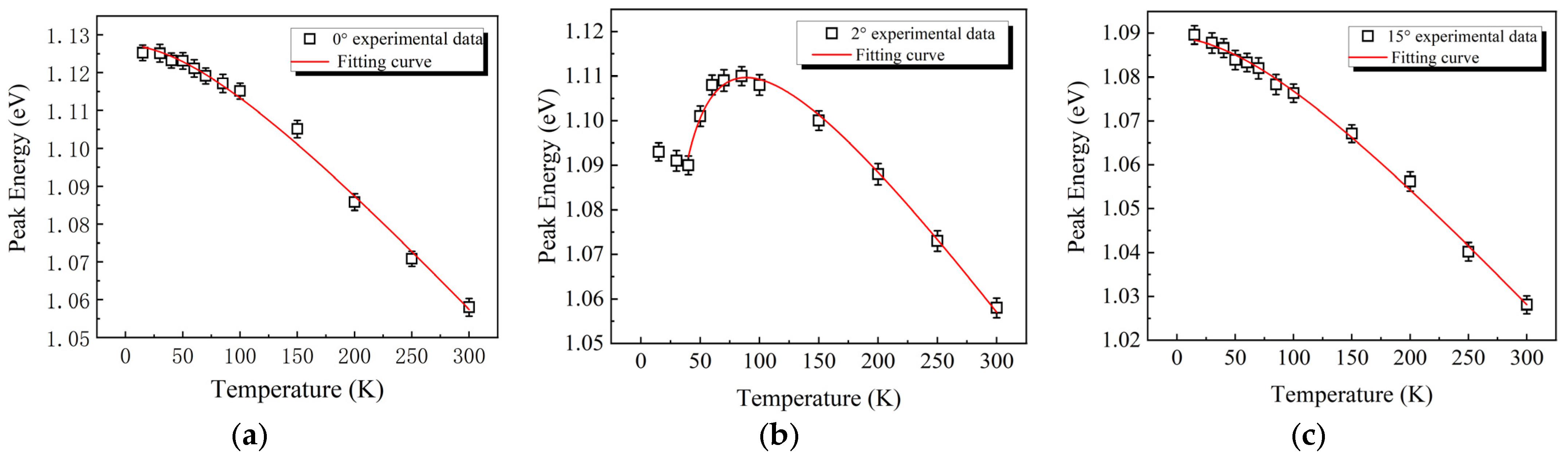
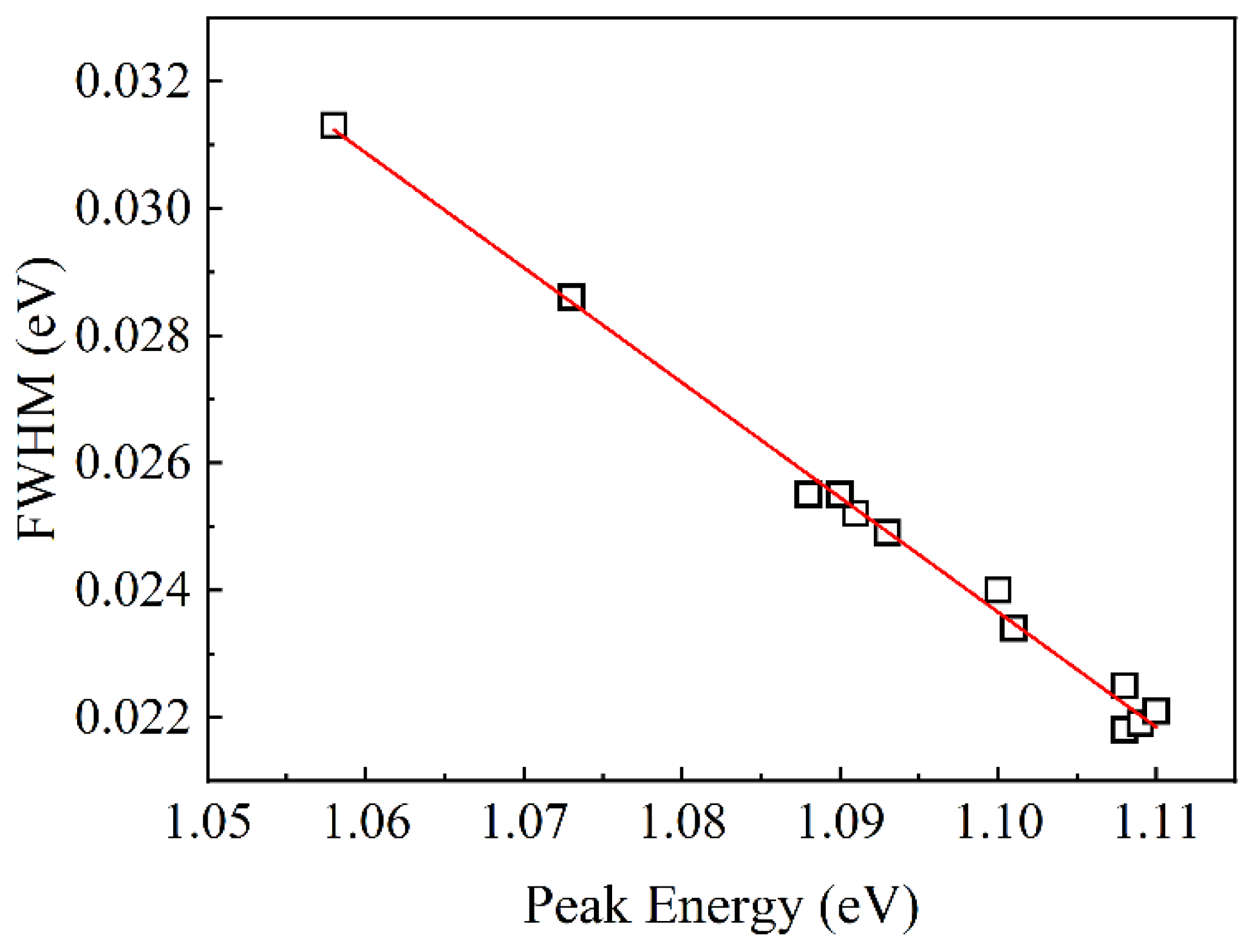
| Sample | Eg(0) (eV) | α (eV/K) | β (K) | σ (meV) |
|---|---|---|---|---|
| 0° | 1.127 | 3.49 × 10⁻⁴ | 150 | |
| 2° | 1.153 | 4.03 × 10⁻⁴ | 109 | 14.7 |
| 15° | 1.089 | 2.84 × 10⁻⁴ | 120 |
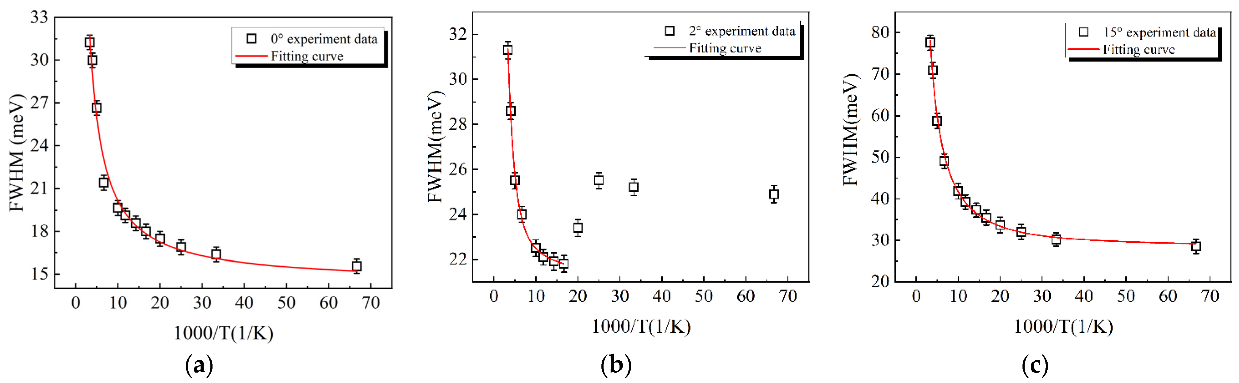
| Sample | Γ0 (meV) | a (meV/K) | γ (meV) | ELO (meV) |
|---|---|---|---|---|
| 0° | 14.36 | 0.058 | 1 | 0.83 |
| 2° | 20.91 | 0.015 | 43 | 0.05 |
| 15° | 28.00 | 0.081 | 12 | 0.01 |
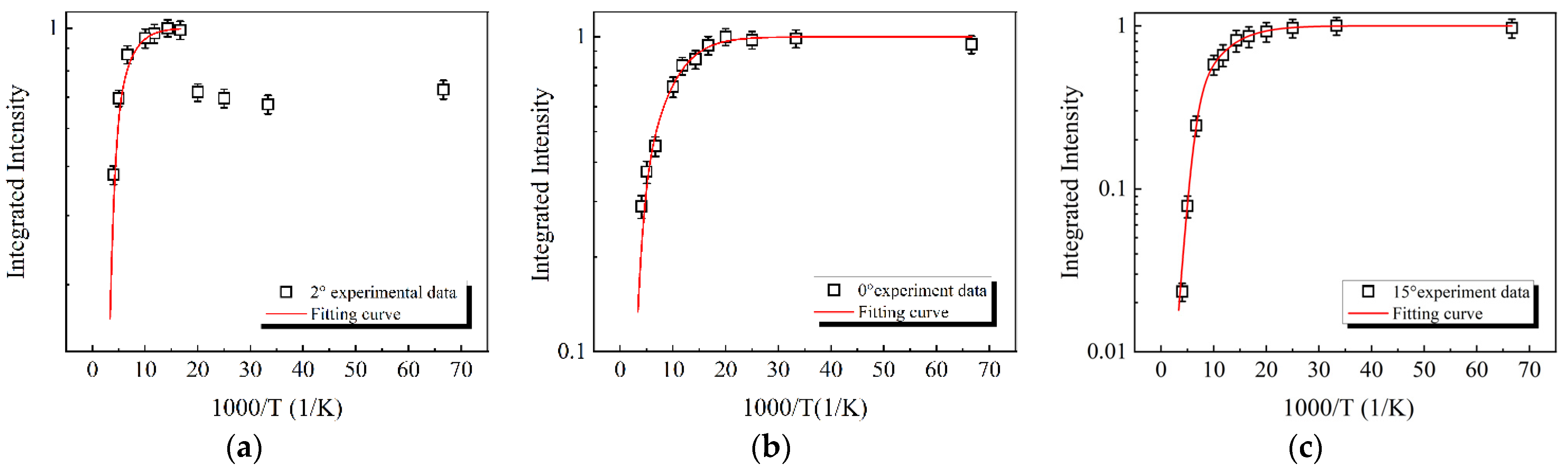
| Sample | C1 | EA (meV) | C2 | EB (meV) |
|---|---|---|---|---|
| 0° | 5.30 | 21.72 | 260 | 106.55 |
| 2° | 4.01 | 35.25 | 1100 | 148.47 |
| 15° | 5.96 | 18.72 | 1525 | 87.26 |
Publisher’s Note: MDPI stays neutral with regard to jurisdictional claims in published maps and institutional affiliations. |
© 2021 by the authors. Licensee MDPI, Basel, Switzerland. This article is an open access article distributed under the terms and conditions of the Creative Commons Attribution (CC BY) license (https://creativecommons.org/licenses/by/4.0/).
Share and Cite
Li, Z.; Zeng, Y.; Song, Y.; Zhang, J.; Zhou, Y.; Ning, Y.; Qin, L.; Wang, L. Effect of Substrate Misorientation on the Structural and Optical Characteristics of In-Rich InGaAs/GaAsP Quantum Wells. Appl. Sci. 2021, 11, 8639. https://0-doi-org.brum.beds.ac.uk/10.3390/app11188639
Li Z, Zeng Y, Song Y, Zhang J, Zhou Y, Ning Y, Qin L, Wang L. Effect of Substrate Misorientation on the Structural and Optical Characteristics of In-Rich InGaAs/GaAsP Quantum Wells. Applied Sciences. 2021; 11(18):8639. https://0-doi-org.brum.beds.ac.uk/10.3390/app11188639
Chicago/Turabian StyleLi, Zhiwei, Yugang Zeng, Yue Song, Jianwei Zhang, Yinli Zhou, Yongqiang Ning, Li Qin, and Lijun Wang. 2021. "Effect of Substrate Misorientation on the Structural and Optical Characteristics of In-Rich InGaAs/GaAsP Quantum Wells" Applied Sciences 11, no. 18: 8639. https://0-doi-org.brum.beds.ac.uk/10.3390/app11188639