Article

Design of SWB Antenna with Triple Band Notch Characteristics for Multipurpose Wireless Applications

1
School of Electronics and Communication Engineering, Reva University, Bangalore 560064, India
2
Department of Electronics and Communication, Manipal Institute of Technology, Manipal Academy of Higher Education, Manipal, Karnataka 576104, India
3
MMRFIC Technology Pvt Ltd., Bangalore 560016, India
4
Department of Information Technology, Sikkim Manipal Institute of Technology, Sikkim Manipal University, Sikkim 737102, India
5
Discipline of Electrical, Electronic and Computer Engineering, University of KwaZulu-Natal, Durban 4041, South Africa
6
Fractus Antennas, 08174 Barcelona, Spain
7
Electronics and Telecommunication Department, Universitat Ramon LLull, 08022 Barcelona, Spain
*
Authors to whom correspondence should be addressed.
Submission received: 8 December 2020 / Revised: 2 January 2021 / Accepted: 4 January 2021 / Published: 13 January 2021
(This article belongs to the Special Issue New Trends in Telecommunications Engineering)

Abstract

:
A compact concentric structured monopole antenna for super wide band (SWB) applications with triple notch band characteristics is designed and experimentally validated. The antenna covers an immense impedance bandwidth (1.6–47.5 GHz) with sharp triple notch bands at 1.8–2.2 GHz, 4–7.2 GHz, and 9.8–10.4 GHz to eliminate interference from co-existing advanced wireless services (AWS), C bands, and X bands, respectively. By loading an E-shaped stub connected at the top of the patch and by etching a split elliptical slot at the lower end of the radiating patch, the band rejection characteristics from 1.8–2.2 GHz for the AWS and 4–7.2 GHz for the C band are achieved, respectively. Further, by making use of a C-shaped resonator near the feed line, band rejection from 9.8–10.4 GHz for the X band is obtained. By varying the parameters of the antenna, the notch bands are controlled independently over a wide range of frequencies. The antenna provides good radiation characteristics, constant group delay response, and better gain over the pass band. The experimental results indicate that the designed antenna offers a remarkable reduction in gain and high variation in group delay over the stop bands. To characterize the wideband property and linear phase response of the designed antenna, its time-domain performance is extensively described and evaluated, which assure pulse transmission with minimum distortion.

1. Introduction

1.1. Motivation

In recent years, wireless communication systems have grown at a significant rate. Wireless consoles for future applications are necessary to support distinct services. This increasing demand leads to the requirement for antennas that are able to cover multiple bands for accommodating several communication standards within a single system in consideration of the fact that the frequency spectrum allocated for ultrawideband (UWB) by the Federal Communications Commission (FCC) is from 3.1 to 10.6 GHz. There is a requirement for a competent super wide band (SWB) antenna that should be capable of functioning over the entire ultra-wide band, as assigned by the FCC, and that should cover lower frequency bands. However, the SWB system broad frequency range may influence the present narrowband systems. Therefore, to alleviate the electromagnetic interference effect of an SWB system over the narrowband system and vice-versa, an SWB antenna with a band-notch feature is desirable for coexisting wireless communications.
A conventional approach for preventing intervention among the recently designed and present-day communication systems is to insert filter banks in the SWB system to filter out the interfering EM waves of different frequencies. However, introducing external band stop filters to accomplish the desired band rejection makes the system complex and enhances the dimension significantly.
Another efficient way for suppressing interfering electromagnetic spectrums from the SWB system is to realize SWB antennas with frequency blocking ability. Antenna shape and structure orientation are two important aspects in designing this type of antenna structure. Several wideband antennas are reported in the literature with no notch, single notch, or dual notch functions. Nevertheless, there is a need to develop SWB antennas with a greater number of notch bands to establish multiple coexisting communications. However, it is very challenging to design an SWB antenna with multi notch bands due to the difficulty in bandwidth control of notch bands while maintaining space limitation and unwanted mutual coupling between the adjacent notched bands.

1.2. Literature Review

The major difficulty in implementing an SWB communication system is eliminating the authorized and unauthorized license bands such as WiMAX, WLAN, AWS, C, X, etc., from the assigned SWB bandwidth. Each of these communications has its defined frequency bands, and the SWB system has to separate out those bands to make the communication interference resistant.
Various researchers have addressed the aforementioned challenge to some extent by introducing SWB antennas with multi notch characteristics. Several techniques such as the introduction of a slot in the patch/ground plane [1,2,3]; insertion of a slit on the patch/ground plane [4,5]; placing stubs [6,7,8,9], meander grounded stubs [10], and parasitic elements [11,12,13]; and employing a split ring resonator [14,15] have been used in SWB antenna design to filter out undesired frequency bands.
Placing a slot on the patch or ground plane empirically helps to reject a particular frequency band and thus brings band notch characteristics to the SWB antenna. Various shapes and sizes of slots have been investigated, and combinations of slots with other geometries have been examined for rejecting a desired band of frequencies. In [1], the bandwidth of a square-shaped antenna was enhanced by placing a dumbbell-structured parasitic resonator at the upper side of the partial ground plane. Further, by adding two similar inverted J-shaped slots and a reverse F-shaped slot, two notch bands were obtained at 3.3–4.2 GHz and 5.1–5.4 GHz frequencies. Again, in [2], a triple notch band SWB antenna was designed by exploring the slot on patch concept. First, a notch band at 3.5 GHz (WiMAX) was realized by cutting an E-shaped slot in the upper portion of the antenna, while a rectangular slot and a C-shaped slot along with a set of two parasitic patches provided two more notch bands at 5.2 GHz and 5.8 GHz (lower and upper) WLAN, respectively. A monopole printed circular radiating patch with a coplanar waveguide (CPW)-fed bevel-shaped ground plane is demonstrated in [3]. By etching two C-shaped slots on the radiating patch and a pair of C-shaped slots in the ground plane, three frequency bands, namely 3.43–3.65 GHz, 4.95–5.25 GHz, and 5.36–5.85 GHz, were eliminated.
Introduction of slits on the patch results in multiband frequency operation because of the disruption caused to the average current paths of any resonant mode. The surface current paths become elaborated around the slits, and because of this, resonant frequency decreases leading to multiband frequency operation. In [4], a modified circular radiating patch with a pair of open ended quarter wavelength slits was realized to suppress dual notch bands of 5.15–5.35 GHz and 5.725–5.825 GHz. In another example of the slit concept, a CPW-fed single band notch circular fashioned antenna was demonstrated in [5]. With the help of a set of stubs and slits adopted inside the tapered slot and circular patch, a notch band of 5.0–5.8 GHz was realized.
Another method to bring notches in wideband antennas is by loading the stub on the antenna structure. Stub loading on the patch or ground plane transfuses the fundamental and harmonics in quadrature and thus eliminates the required band of frequencies. Jiang et.al. presented a square-shaped radiating patch with a modified ground plane for developing a dual notch band wideband antenna. By introducing an inverted T-shaped stub on the patch and a set of U-shaped stubs adjacent to the feed line, stop bands of 3.3–4.0 GHz (WiMAX) and 5.05–5.90 GHz (WLAN) were achieved [6]. In [7], a quasi-U-shaped patch with a stepped slot in the ground plane was presented to bring wide bandwidth in antenna characteristics. Two inverted L-shaped stubs in the radiating patch realized two notch bands of 4.97–5.48 GHz and 5.69–5.99 GHz for removing lower and upper WLAN bands, respectively. A guitar-shaped CPW-fed monopole radiator with triple band notch functionality was presented by Sharma et al. [8]. By adding an inverted T-shaped stub and a pair of elliptical slots on the radiator, three interfering frequencies of 3.74 GHz (under WiMAX band), 5.45 GHz (under WLAN band), and 7.65 GHz (under X band) were eliminated. In [9], by embedding a fractal stub on the radiating patch and by etching a pair of modified rectangular slots, triple notch bands from WiMAX (3.30–3.80 GHz), WLAN (5.150–5.825 GHz), and DSS (7.25–7.75 GHz) were encountered.
Alternately, meander lines have also been used for notch antenna design, because they resonate at different independent frequencies. Meandering means turning or winding. If the number of turns are increased, the meander stub resonates at lower frequencies, and vice versa. It is well known fact that the surface current primarily distributes at the periphery of the microstrip line, and in the meander stubs, the magnitude of surface current will be greater at the corners/bending portion, which provides a coupling to the microstrip line, thus providing the notch at that particular frequency. In [10], a microstrip-fed elliptical-shaped planar monopole antenna with three notch band properties was demonstrated. With the aid of three sets of meandered ground stubs, triple notch band characteristics were obtained. Two notch bands of 3.3–3.6 GHz and 5.15–5.35 GHz were derived from two sets of meandered stubs near the feedline, and another notch band of 5.725–5.825 GHz was yielded from a meandered stub on the upper edge of the ground plane. Another technique to obtain notch bands in a wideband antenna is by introducing parasitic elements near the radiator. A parasitic element is an element that operates under the influence of other’s feed. The parasitic element behaves like a passive resonator that modifies the radiation pattern emitted by the patch antenna. Thus, the parasitic element helps to provide wideband characteristics and notch functionality. Yadav et al. [11], presented a circular monopole radiator with a parasitic resonator for adding wideband characteristics. By embedding I-shaped and inverted-U-shaped parasitic resonators at the rear side of the radiating patch, dual band notch functions at 5–5.35 GHz and 7.85–8.4 GHz were achieved. Wide bandwidth was also achieved by introducing parasitic elements in addition to slot concepts in antenna design. A tapered triangular microstrip-fed circular monopole antenna with dual band notch characteristics was demonstrated by exploring the parasitic element and slot concept in [12]. By inserting a U-shaped parasitic component in proximity of the ground plane and an inverted T-shaped stub inscribed within the patch, a first stop band at 3.2–4.4 GHz was obtained. For the second stop band at 7.2–8.4 GHz, a U-shaped slot was etched out from the ground plane. Another illustration of a parasitic element-based wideband antenna with band notch characteristics can be seen in [13], where a hemi ellipse-shaped radiating patch with a parasitic element and an elliptical slot was used to hold a single notch band (5.15–5.825 GHz) in the complete frequency band of 3–17 GHz.
In another approach, a split ring resonator (SRR) and complementary SRR (CSRR) have been significantly used for designing antenna with band notch capability. The SRR and CSRR can produce strong electric and magnetic coupling from LC resonance and thus are used for band stop filter modelling. In [14], by etching two CSRRs on the radiating patch and by using a set of rectangular SRRs beside the feed line, three notch bands of 3.3–3.8 GHz (Wi-MAX), 5.15–5.85 GHz (WLAN), and 7.9–8.4 GHz (X-band) were brought in the complete frequency band of 2.21–11.71 GHz. In another example of a CSRR-based wideband antenna, a miniaturized microstrip-fed planar monopole antenna with three band notch features was designed by Sarkar et al. [15]. There, triple band notch (3.4 GHz, 5.2 GHz, and 5.8 GHz) functionality was achieved by defining a set of slots around the edges of the patch, a circular-shaped CSRR at the center of the patch, and a set of rectangular-shaped CSRRs on either side of the ground.
The techniques presented in the foregoing discussion are able to create single or multiple notch bands for wideband planar antennas. It has been observed that most of these wideband antennas are able to accommodate frequencies up to 20 GHz, but present-day requirements of many wireless communications such as Ka band satellite, 5G, 6G, etc., are beyond this range. Therefore, there is a need to design an SWB antenna that can support communication beyond 20 GHz. At the same time, the SWB antenna needs to be interference resistant for establishing coexisting communication. Therefore, in addition to increasing bandwidth for the SWB antenna, multiple notch characteristics need to be implemented to avoid interference from licensed and unlicensed existing communications.
Another major concern that has not been addressed by the majority of existing research on wideband antennas is the time-domain characterization that includes measurements of group delay, impulse response, system fidelity factor, etc. Time-domain characterization of the SWB antenna has a greater significance, as those antennas exploit a severe influence on the waveforms.

1.3. Contributions

In this work, design and analysis of an SWB antenna with triple band notch characteristics for multiple wireless applications are presented. The designed antenna is capable of removing three interfering bands at advanced wireless services (AWS), and C and X band systems.
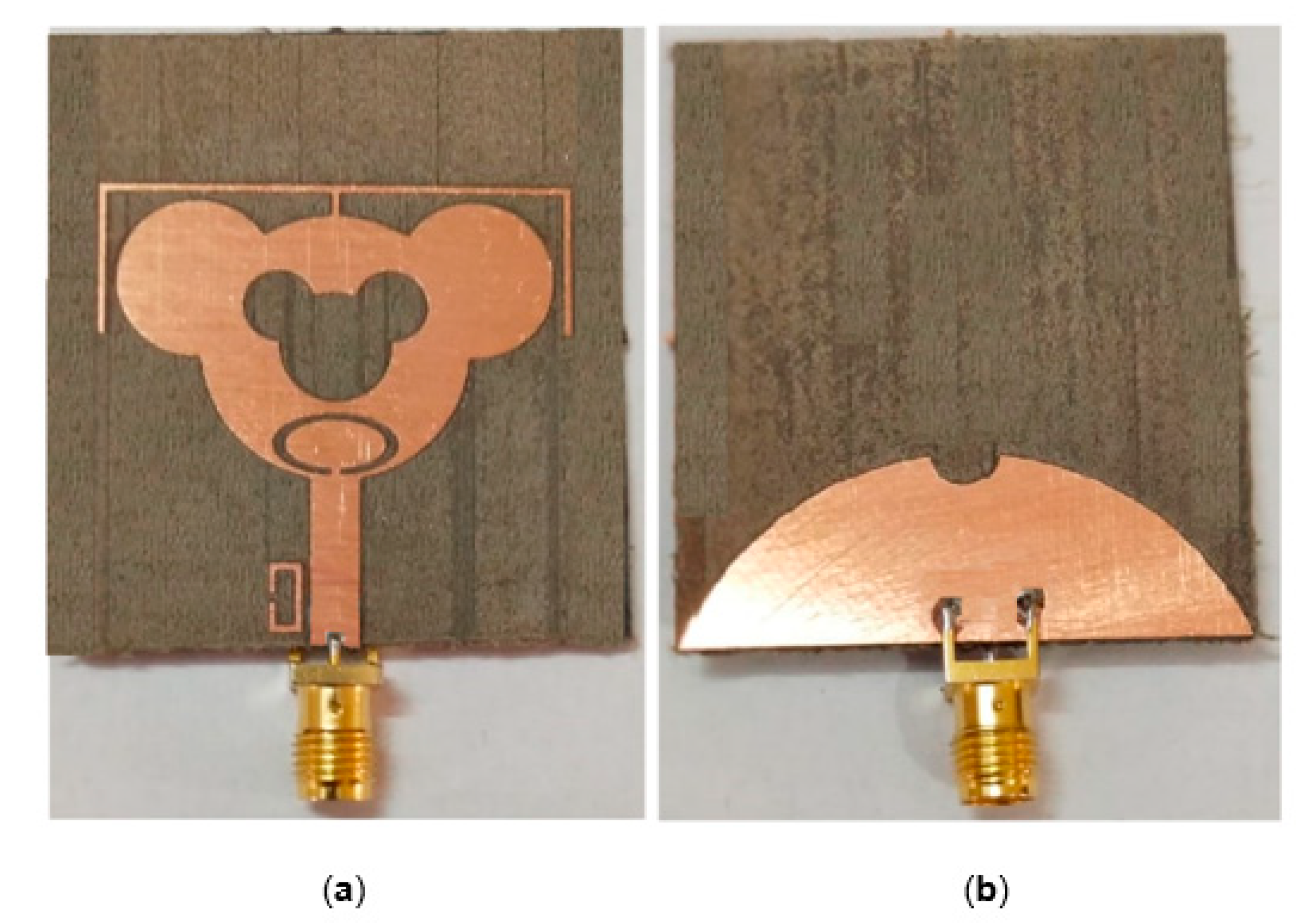
  • To attain the notched frequency band for AWS (1.8–2.2 GHz), an E-shaped stub is loaded on the top of the radiator.
  • A split elliptical slot at the base of the radiating patch is used to achieve a band notch at the C band (4–7.2 GHz).
  • By placing a C-shaped resonator near the feed, a band notch at the X band (9.8–10.4 GHz) is acquired.
The main prominence of the designed radiator is its very wide bandwidth and large bandwidth dimension ratio (BDR), which is obtained by modifying the electrical length of the radiator. The presented antenna structure attains a frequency range of 1.67–47.5 GHz (VSWR < 2) with a bandwidth ratio of 28.44:1 and a fractional bandwidth of 186%. The results are captured by simulating the model in HFSS 19.0 software.
This paper is organized into different sections as follows: The first section presents an introduction to the band-notched SWB antenna. The design steps and characteristics of the proposed antenna are investigated in Section 2. Significant parameters that control the bandwidth and impedance matching are illustrated in Section 3. Then the simulated and experimental results viz. current distribution, gain, and radiation patterns are illustrated in Section 4. Section 5 focuses on modelling of equivalent circuit for the proposed antenna. Time-domain characteristics, namely system fidelity factor (SFF), group delay, and transfer function, are presented in Section 6. Section 7 highlights the main features of the proposed SWB antenna by including a comparative analysis. Finally, the paper is concluded in Section 8.

2. Design Methodology

The geometry of the proposed SWB monopole antenna with triple band-notched characteristics is depicted in Figure 1, its related parameters are indexed in Table 1, and the configuration is detailed analysis has been given in [16]. The antenna was implemented on a Rogers RT-Duroid 5880 substrate with dielectric constant of 2.2, tan δ = 0.0009, and thickness of 1.57 mm. A procedural evaluation of the presented antenna was carried out in order to analyze the behavior of the designed antenna at particular steps. The main purpose of describing the present section is to explain the technique for obtaining three notched interfering bands at the coinciding frequencies. This section also clarifies the outcome of each notch-creating configuration on the functioning of the reference antenna. Each individual stage illustrates the characteristics of the antenna in terms of VSWR.
In phase 1, a microstrip-fed structural monopole antenna for SWB application is examined. In the second phase, design and exploration of the SWB antenna with a single notch-band is exhibited. In the third phase, a printed SWB antenna is described with dual-band notch characteristics at two unique interference bands. In the final phase, a planar SWB antenna with triple band notch properties is introduced. The notch bands can be independently tuned to reject individual frequency bands.

2.1. Phase 1: Design of Super Wideband Antenna (Antenna 1)

A microstrip-fed printed monopole antenna for SWB application is used. The proposed antenna is derived from a conventional circular monopole antenna. To achieve wide bandwidth and matching, a conventional circular monopole antenna was modified by adjoining a pair of ears at the upper part of the radiator and also by modifying its partial ground plane. The anatomy of the designed SWB antenna and its corresponding VSWR variation over frequency are displayed in Figure 2. The values of VSWR between 1 and 2 throughout the frequency range (1.2–47.5 GHz) depicts good impedance matching for the proposed SWB antenna. Since there is no predefined standard frequency spectrum for SWB antenna structures, a comparison between the wideband antenna structures can be made in terms of an index term, i.e., the bandwidth dimension ratio (BDR) [16], which defines the antenna bandwidth (in percentage) per unit area of the antenna. The following equation is used for BDR calculation:
B D R = B W % λ l e n g t h × λ w i d t h
where, λ w i d t h and λ l e n g t h are the electrical width and length, respectively, of the antenna in the context of wavelength associated with the lower cut-off frequency, and B W % is percentage bandwidth considering a VSWR ≤ 2. The designed antenna structure achieved a total bandwidth range of 1.2–47.5 GHz (VSWR < 2) along with a BDR of 38.9:1 and a fractional bandwidth of 190%.

2.2. Phase 2: Design of Single Notched Band SWB Antenna (Antenna 2)

The most critical concern in the design of a band-notched SWB antenna is the deployment of its notch-forming configurations to prevent nearby existing bands. The notch-band centered at 2 GHz (AWS), covering the frequency range of 1.8–2.2 GHz was prevented by placing an E-shaped stub on the top of the radiator. The antenna with a single band notch feature is presented in Figure 3. It can be noted that the dimensions of the reference designed SWB antenna (Antenna 1) remained unaltered when the notch-creating configuration was included with the reference antenna. Therefore, no re-tuning was needed for the reference SWB antenna for introducing the notch characteristics. The simulated VSWR of single-notched band SWB antenna, as shown in Figure 3, demonstrated the rejection of the frequency band of 1.8–2.2 GHz from the entire band of 1.2–47.5 GHz.

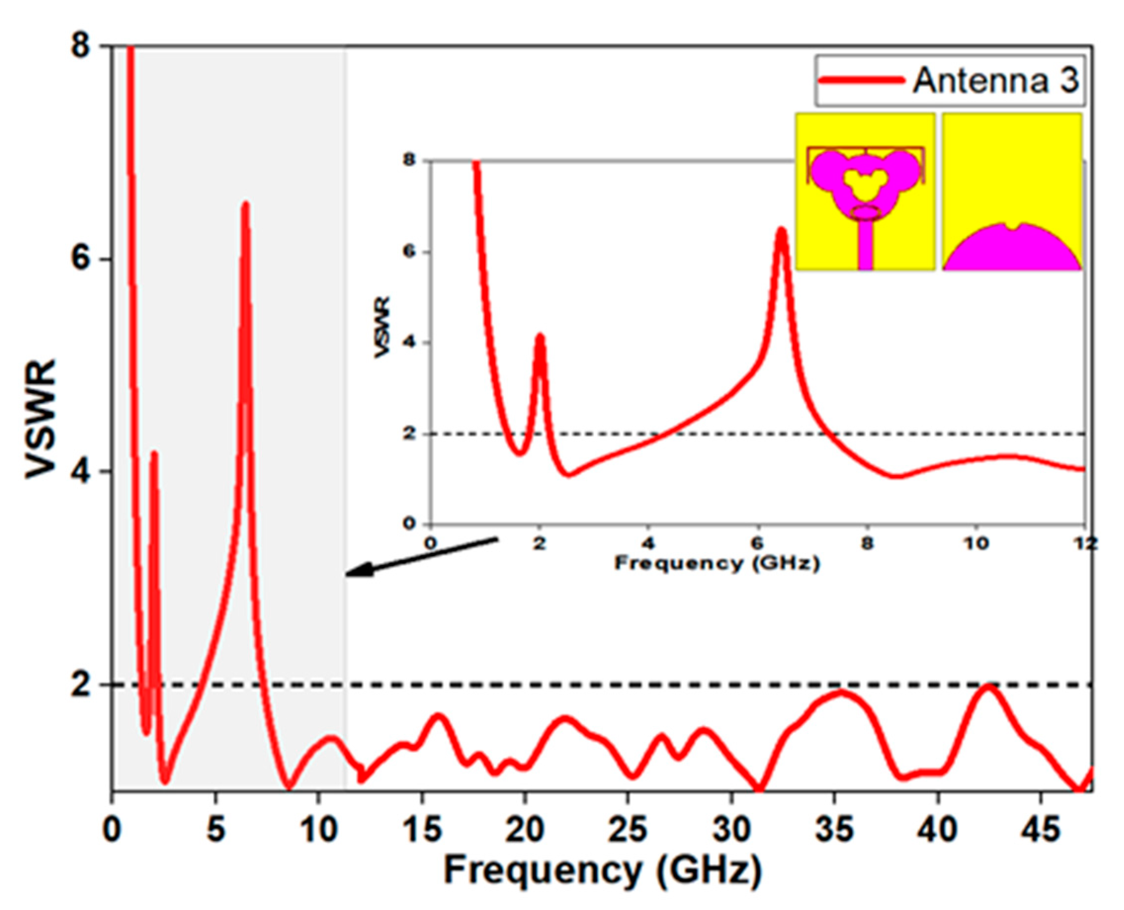
2.3. Phase 3: Design of Dual Band-Notched SWB Antenna (Antenna 3)

To deal with undesirable possible intervening of the narrowband regime with the SWB antenna, another intervention band in extension with the AWS band was created at 6 GHz, which was capable of covering the bandwidth of 4–7.2 GHz (C band). A split elliptical-shaped slot was engraved at the lower edge of the patch to stop the C band. Figure 4 represents the antenna structure with two band-notches and its VSWR result. From the VSWR graph, we can deduce that the second band notch introduced in the antenna structure did not affect the efficacy of the single band notch (Antenna 2).

2.4. Phase 4: Design of Triple Band-Notched SWB Antenna (Proposed Antenna)

To alleviate the interference at X band, a C-shaped resonator was placed at the bottom of the patch beside the feedline. The addition of the C-shaped resonator led to the obstruction of the X band (9.8–10.4 GHz) without influencing the efficacy of Antenna 3. Figure 5 illustrates the proposed antenna configuration and VSWR result of the triple band-notched antenna. The designed antenna exhibited a wide bandwidth, including a triple notch band feature with a very compact design.

3. Parametric Analysis

A parametric study was conducted for optimizing numerous design parameters. A comprehensive behavioral analysis of the designed antenna was accomplished with a view to evaluating the efficacy of the antenna and to identify the influencing parameters of the respective notch band. The impact of the notching factors on the respective notches was investigated thoroughly, whereas the rest of the factors remained unaltered.

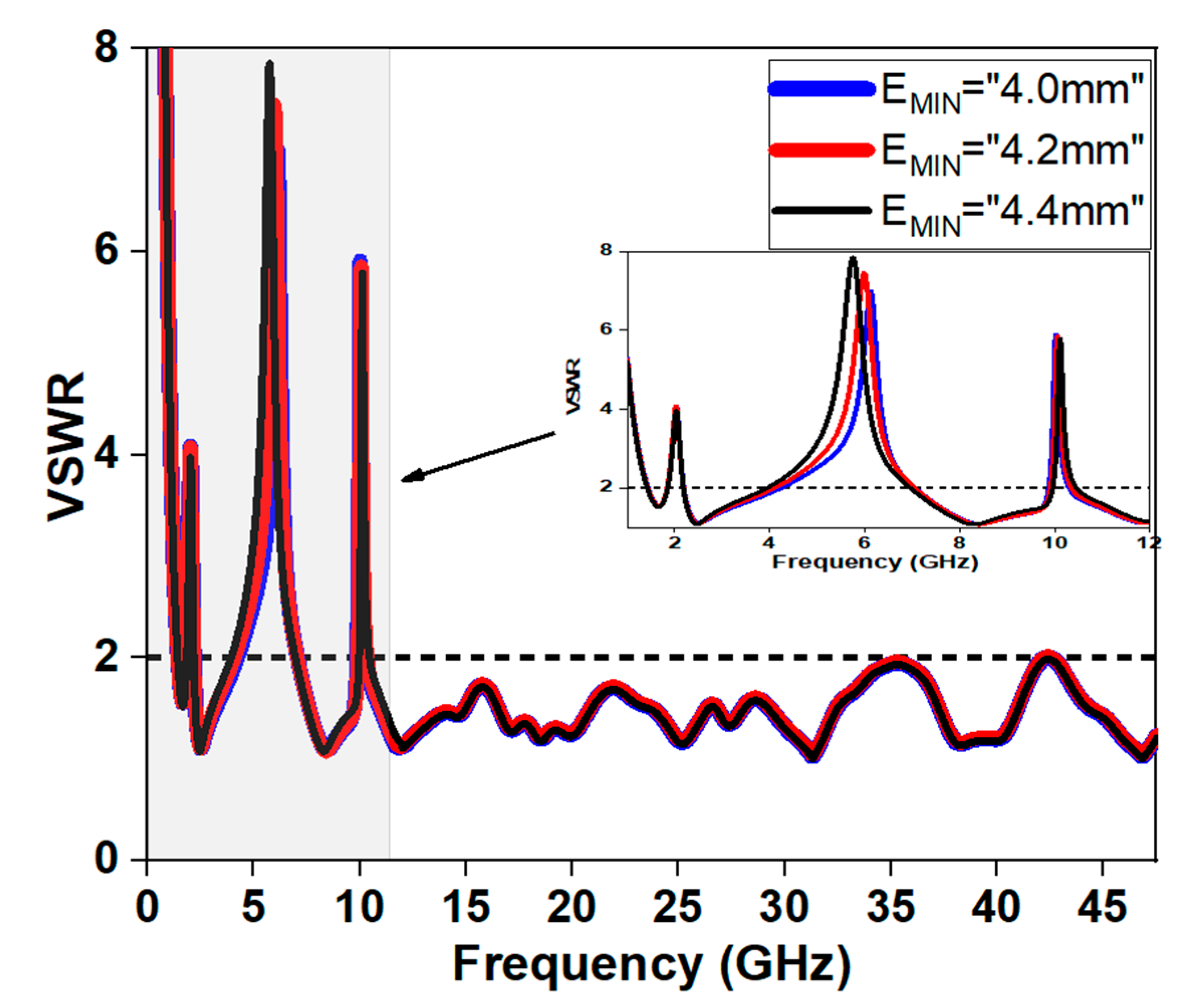
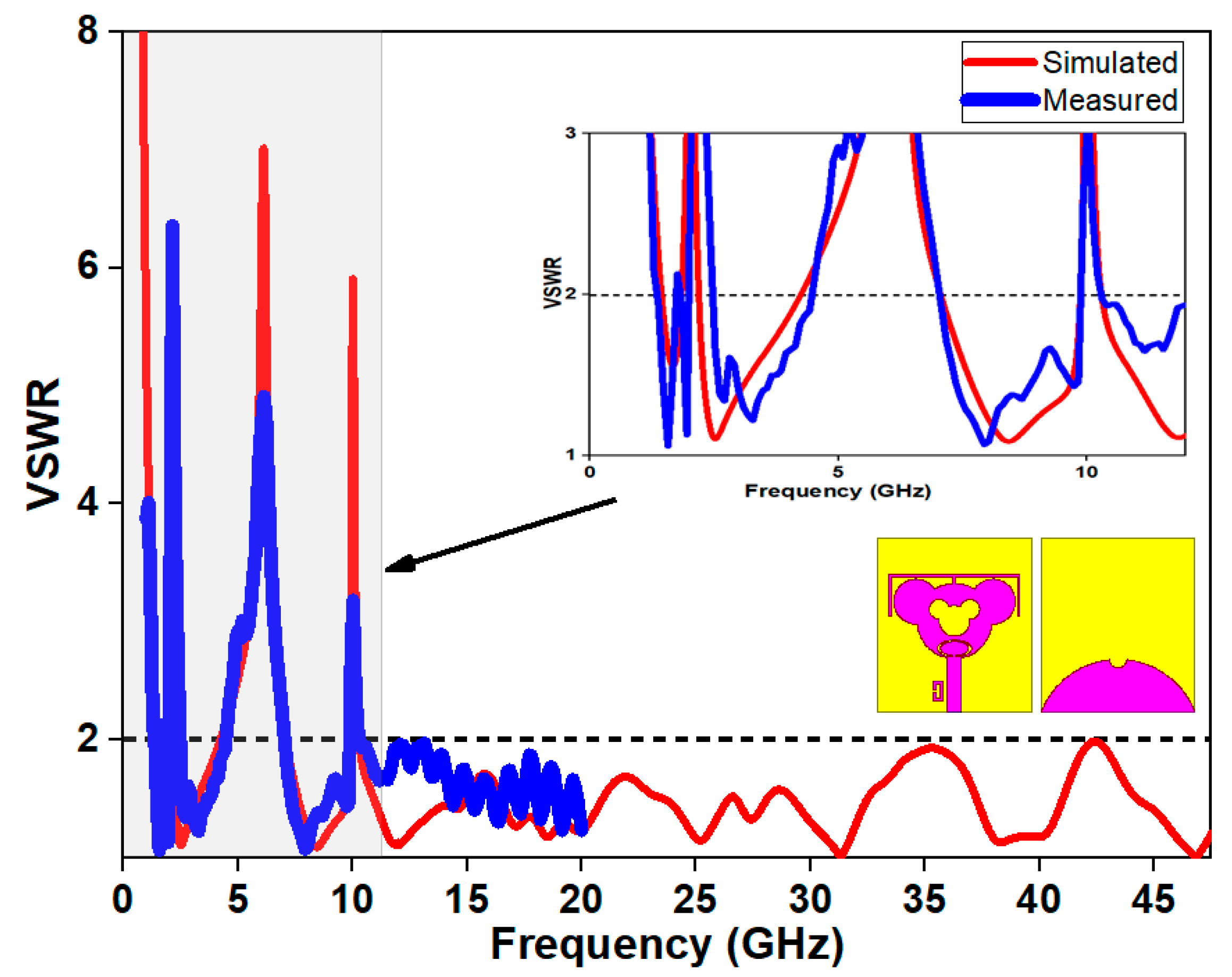
3.1. Independently Controllable Notch AWS Band (1.8–2.2 GHz)

Figure 6 illustrates the optimization of an “E“-shaped stub accountable for mitigating AWS (1.8–2.2 GHz) interference. It is evident from Figure 6 that E2 was the controlling parameter of the notch for the AWS band of the proposed antenna.
L s t u b = c 2 f n o t c h ε e f f
ε e f f = ε r + 1 2
For the optimized dimension of E2 = 10 mm, the first frequency band notch was centered at 2 GHz, the second frequency band notch was centered at 6 GHz, and the third frequency notch was centered at 10 GHz. When the parameter E2 was modified from 8 mm to 9 mm, the first notch band shifted in the regime of the higher frequency range, whereas the second and third notch bands remained unaltered. The optimized equation of the “E“-shaped stub affecting the AWS wireless communication system is given by Equation (2), where (E1 = 34 mm, E2 = 10 mm, E3 = 1.2 mm) is the stub length, ε r is relative permittivity, ε e f f is effective dielectric constant of the substrate calculated using Equation (3), “ c ” corresponds to the speed of light, and f n o t c h is the notch center frequency. The theoretically calculated “E”-shaped stub length for 2 GHz is 59.29 mm, while the optimum value for the “E”-shaped stub is 55.2 mm. The detailed parametric variations is illustrated in Table 2.

3.2. Independently Controllable Notch C Band (4–7.2 GHz)

The elliptical slot at the lower radiating portion of the designed antenna was liable for notch creation at the C band. It is apparent from the Figure 7 that parameter EMIN was accountable for governing the notch at the C band. For EMIN = 4 mm, the notch at the C band was at 6.13 GHz. By increasing the value of EMIN from 4 mm to 4.2 mm, the second notch was shifted from 6.13 GHz to 6 GHz. By further increasing the value of EMIN to 4.4 mm, the second notch was reached at 5.97 GHz. In all instances, the first and second notches stayed unaffected by changes in the factor EMIN. It could be stated from the study of the parametric analysis for EMIN that the middle notch could be independently controlled. It was also ascertained that the EMIN parameter did not influence the first frequency notch band (AWS band) or the third frequency notch band (X band).
For a split elliptical slot of major axis length EMAX, minor axis length EMIN, and width ER, the design equations for calculating a band-notch at a given frequency can be represented as Equation (4).
E c = D e π ( 0.5 E M I N E R ) = λ g 2 = c 2 f n o t c h ε e f f
D e = 3 ( 1 + d ) ( 3 + d ) ( 1 + 3 d )
ε e f f = ε r + 1 2 + ε r 1 2 [ 1 + 12 h W F ] 1 2
where, E c represents the inner perimeter of the elliptical slot, which could be equal to half of the directional wavelength at the intended notch frequency. The parameter D e , utilized for the estimation of the perimeter of ellipse, is associated with the ellipticity by “ d ” through Equation (5) (where d = E M A X / E M I N = 1.94), which is obtained as 3.01. The effective dielectric constant is calculated through Equation (6) as 1.84, where h (1.57 mm), W F (3.6 mm), “ ε r ” (2.2) are the substrate height, width of the microstrip feed, and relative permittivity of substrate, respectively. In the design simulations, the width of the slot was fixed at E R = 0.2 mm. To obtain this second band-notch at 6 GHz within the C band (4–7.2 GHz), we chose E M I N = 4.2 mm and E M A X = 8.16 mm. The theoretically computed elliptical slot value ( E c ) for 6 GHz was 18.43 mm, whereas the optimal parameter ( E c ) for the slot was recorded as 18.02 mm.

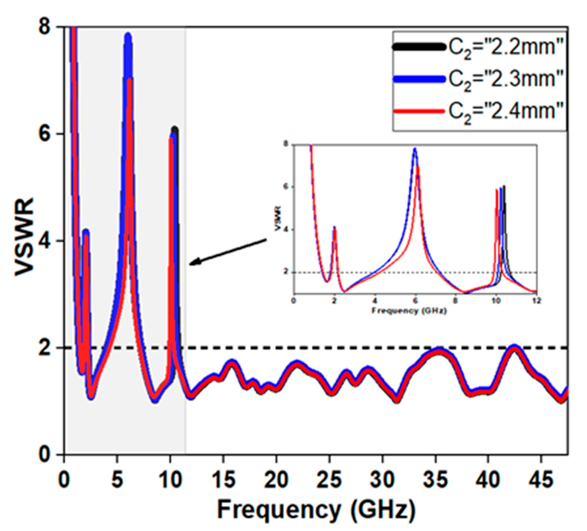
3.3. Independently Controllable Notch X Band (9.8–10.4 GHz)

A C-shaped parasitic resonator was placed near the feed line for mitigating interference at X-band (9.8–10.4 GHz). Similar to the monitoring parameters of the AWS notch band and “C” notch band, parameter C2 was the controlling parameter for the X band.
By altering the values of the parameter C2, the third frequency notch band was shifted, whereas the first and second frequency notch bands remained unaltered. As is depicted in Figure 8, reducing the value of parameter C2 displaced the third notch band towards higher frequencies. The third frequency notch band present at 10.38 GHz for C2 = 2.2 mm was displaced to 10.22 GHz for C2 = 2.3 mm and was shifted to 10 GHz for C2 = 2.4 mm. From the parametric study it was found that C2 had a considerable influence on localizing the third frequency notch band, whereas the remaining notch bands were unaltered. At the intended notched frequency, the length of the parasitic resonator is calculated using the expression given below in Equation (7).
L p a r a s i t i c   r e s o n a t o r = λ g 2 = λ 0 2 ε r e f f = c 2 f n o t c h ε r e f f
ε e f f = ε r + 1 2 + ε r 1 2 [ 1 + 12 h W ] 1 2
The length of the parasitic resonator is equal to C 1 + 2 C 2 + 2 C 3 4 C T , where C1 = 5 mm, C2 = 2.4, C3 = 1.6 mm, CT = 0.54 mm, CG = 0.6 mm, λ0 = c/fnotch is the free space wavelength, “ c ” is the speed of light, “ f n o t c h ” is the center frequency of the notched band, “ ε e f f ” is the effective permittivity, “ ε r ” is the dielectric constant of the substrate, “ h ” is the height of the substrate, and W F is the width of the feed line. The theoretically calculated C -shaped resonator value for 10 GHz is 11.05 mm, while the adjusted value for the resonator is 10.84 mm.

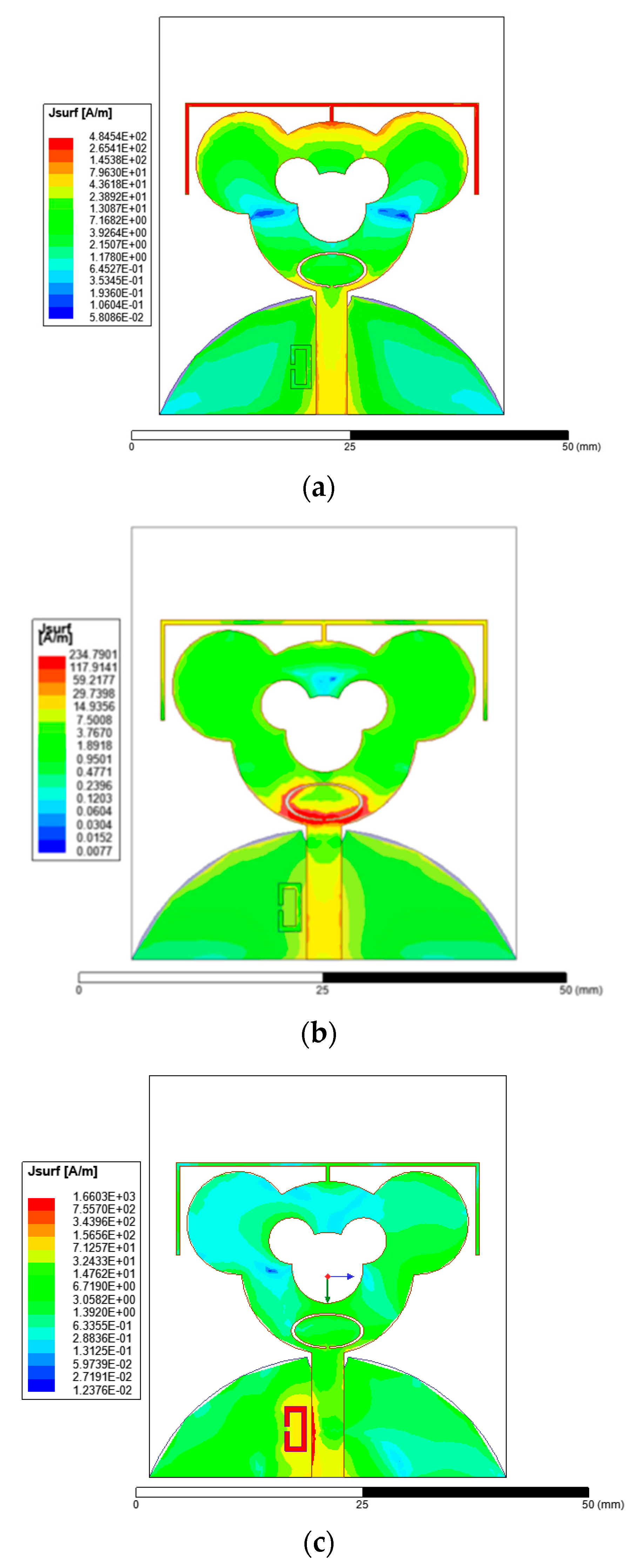
4. Current Distribution Analysis

To realize the creation of notch bands, the current density distribution at three notched frequency bands for AWS, C band, and X band was studied. Figure 9 illustrates the respective elements responsible for the band-notch characteristics. Strong current concentrations around slot, stub, and resonator inferred that there existed high mismatch in impedance, which indicated the creation of notch resonance at corresponding notch frequencies. Figure 9a shows that the maximum current was concentrated within the E-shaped stub intended to notch the AWS band. Figure 9b depicts the surface currents at 6 GHz; the current was largely distributed around the elliptical-shaped slot compared to the other part of the antenna. Figure 9c gives the surface current distribution in the antenna at 10 GHz. A strong current dispersion was examined at the C-shaped resonator for the 10 GHz notched band, which further elucidated that this notch was produced due of the adverse effect of current caused by the C-shaped resonator.

5. Results and Discussion
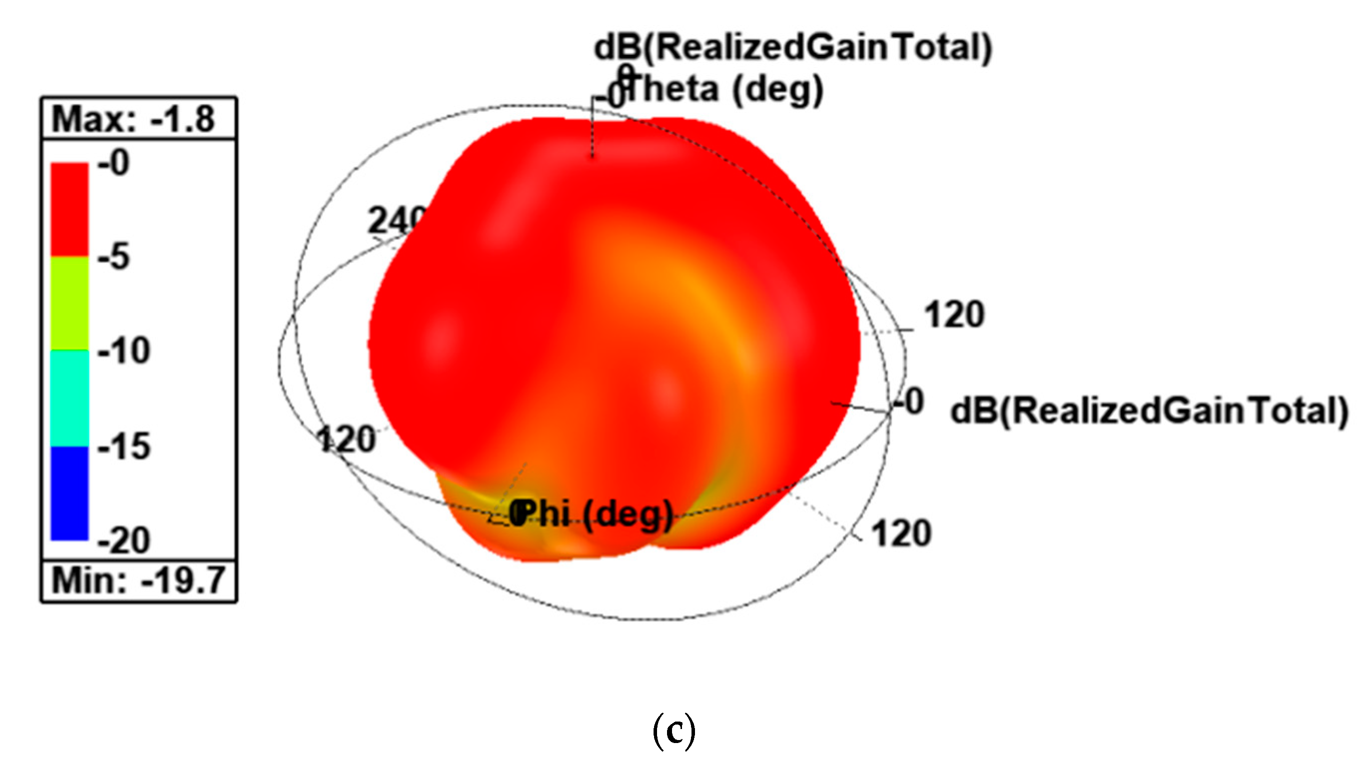
In order to exhibit the efficacy and fulfillment of the designed antenna, a prototype was developed, and experimental measurements were carried out. Figure 10 shows the fabricated triple band-notched SWB antenna in reference to the above-mentioned parameters in Table 1. An Anritsu MS46122B vector network analyzer (VNA) was used to measure the antenna parameters. Even though the designed antenna functioned well for the frequency spectrum of 1.67–47.5 GHz, the empirical results were recorded only up to 20 GHz because of the higher frequency constraints of the available VNA.
Both simulated and measured VSWR results of the presented antenna are provided in Figure 11. Simulated and measured result showed that the designed antenna operated at 1.67–47.5 GHz with VSWR below 2, except the triple notched bands at 1.8–2.2 GHz, 4–7.2 GHz, and 9.8–10.4 GHz for rejecting the AWS and C and X band signals, respectively.

5.1. Gain

The simulated 3D polar gain plot of the designed SWB antenna at the notch resonance frequencies of 2 GHz, 6 GHz, and 10 GHz is presented in Figure 12. Three sharp reductions in the gain at about −9.9 dB, −3.6 dB, and −1.8 dB in the notched bands at 2, 6, and 10 GHz, respectively, were perceived, which evidently proved the signal rejecting ability of the presented antenna.
The gain obtained by simulating the model were proved to be in a positive agreement with measured results achieved from the fabricated prototype of the antenna. Figure 13 exhibits the variation of simulated and measured peak gain with frequency for the proposed antenna over the SWB frequency range (1.67–47.5 GHz). Abrupt gain reductions in the notched band could be anticipated because of elevated VSWR values at these frequencies, which resulted in low gain. At frequencies other than notched bands, the gain of the antenna was enhanced with frequency and increased from 1.7 dB to 10 dB. At notched frequencies, the simulated gain was −9.9 dB, −3.6 dB, and −1.8 dB, whereas the measured gain was −10.38 dB, −4.45 dB, and −2.08 dB at 2 GHz, 6 GHz, and 10 GHz, respectively. (Note: The empirical results were recorded only up to 20 GHz because of the higher frequency constraint of the available VNA).

5.2. Radiation Pattern

With a view to demonstrating that the designed antenna radiated across a broad frequency range, Figure 14 illustrates the simulated and experimented radiation patterns in the H-plane ( = 90 ° ) and E-plane ( = 0 ° ) for the passband resonance frequency of 2.53 GHz, 8.43 GHz, 11.88 GHz, and 18.51 GHz. It can be seen that the proposed antenna presented reasonably good bidirectional monopole E-plane patterns and omni-directional H-plane patterns over the different passband frequencies. At the higher frequencies (greater than 8 GHz), the radiation patterns in both planes were distorted on account of the higher order modes’ excitation and non-uniform phase division. As a consequence, radiated modes may have promoted an increased level of electromagnetic interference (EM). In order to suppress these unwanted radiated modes, a designer can employ techniques such as introducing periodic structures, parasitic elements, split ring resonators (SRRs), etc. However, these techniques increase the complexity of the design and cost of fabrication.

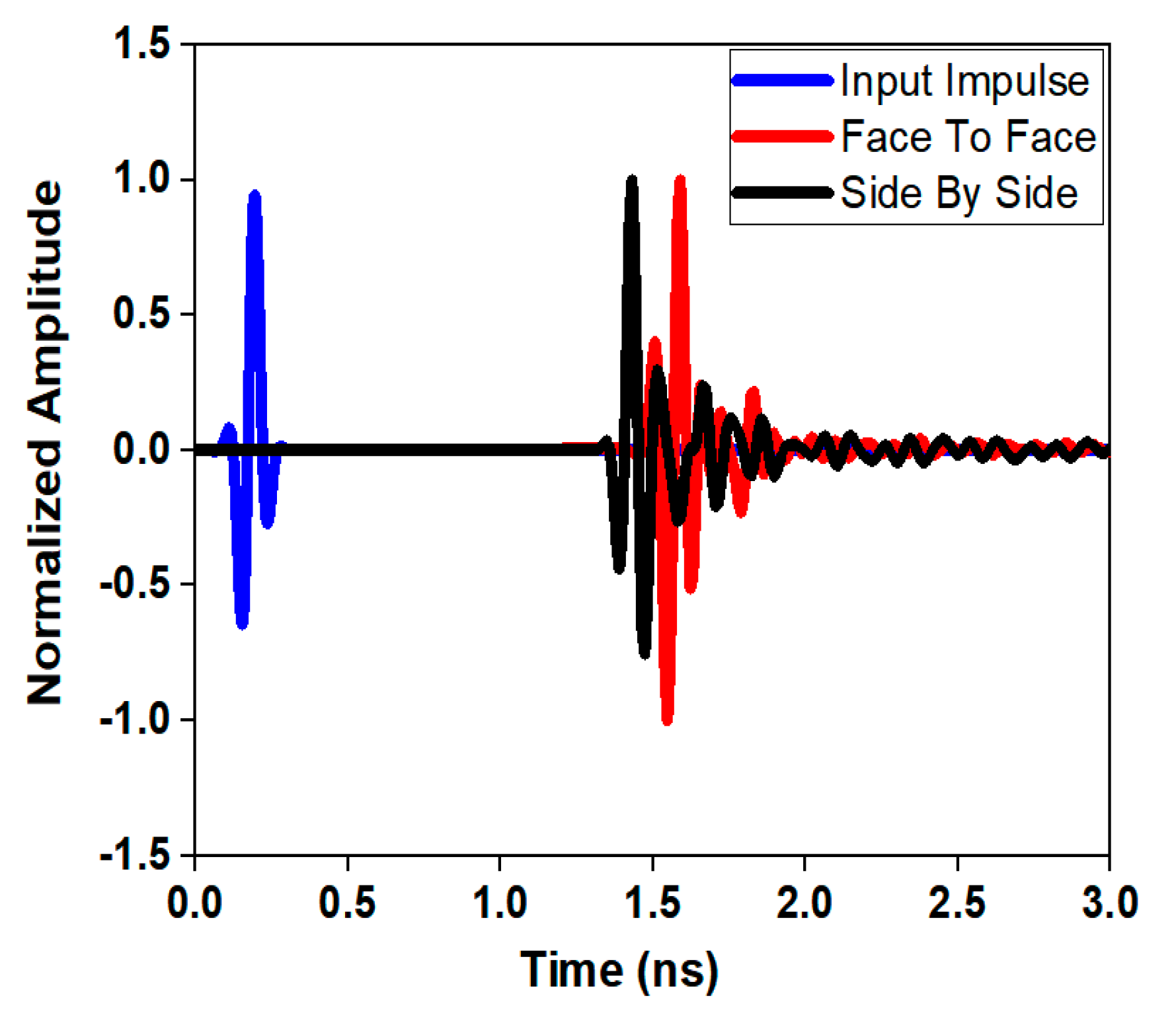
6. Time-Domain Characterization

SWB antennas must be capable of operating over the entire bandwidth with good efficiency and acceptable radiation properties. Simultaneously, the transmitted pulse from the SWB antenna should have a good impulse response with minimum distortion. In addition, it is necessary that the pulse be identified at the receiver end with minimal distortion. Therefore, to endorse the significance of the antenna for pulsed communication systems, time-domain analysis was performed. The time-domain characterization of the antenna parameters confirmed that the designed antenna was an excellent candidate for triple band-notched SWB applications. To realize the time-domain behavior of the signal at band-notched frequencies, two similar antennas were arranged in face-to-face and side-by-side configurations 75 mm apart, as shown in Figure 15. In both the configurations, Gaussian pulses, as shown in Figure 16, were taken into consideration. A few key time-domain metrics were investigated in this following subsection.

6.1. System Fidelity Factor (SFF)
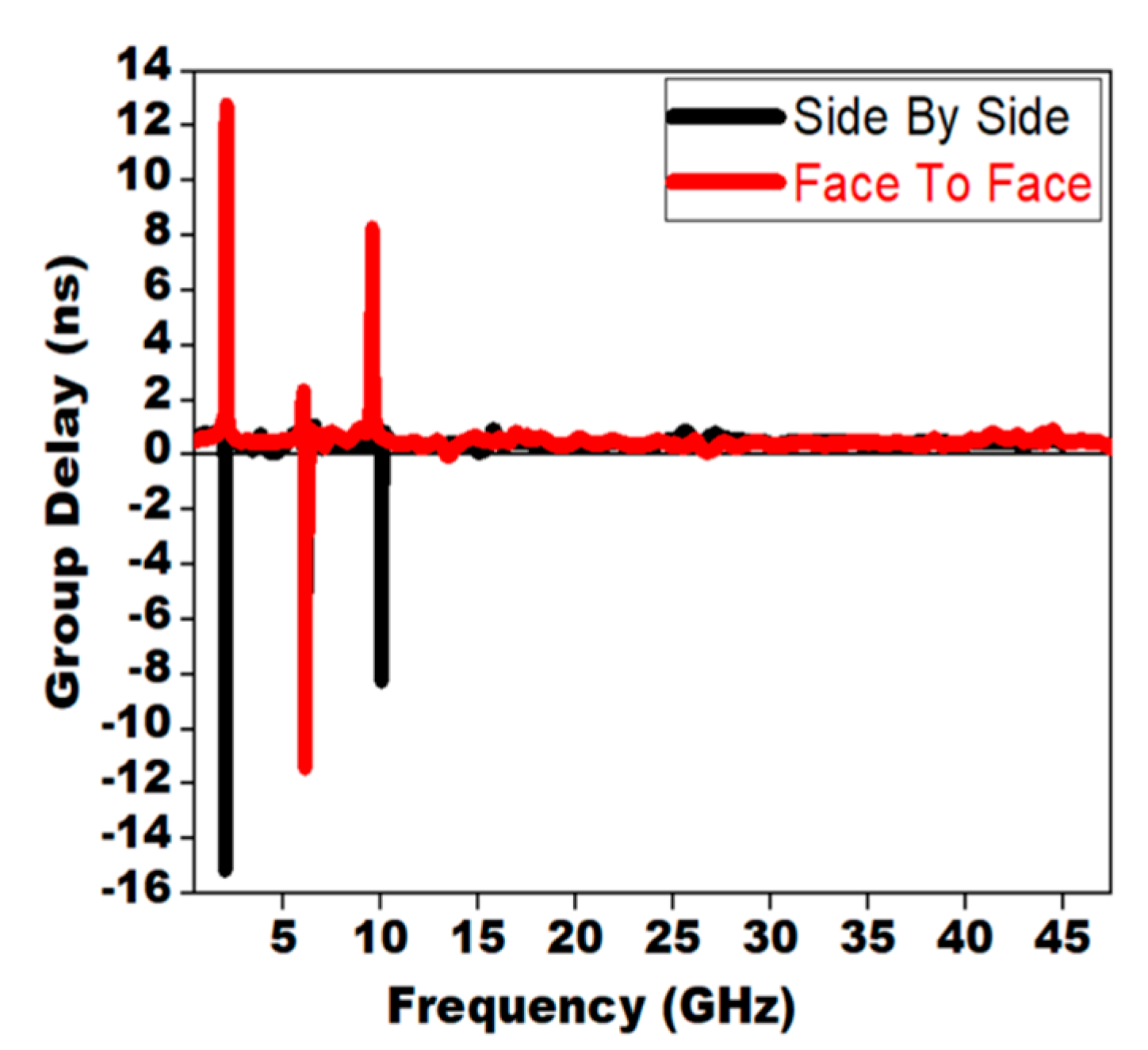
SSF can be described as the cross-correlation between the normalized input waveform Ts(t) and normalized received waveform Rs(t) and can be evaluated by Equation (9)
S F F = max T T s ^ ( t ) R s ^ ( t + τ ) d t
where
T s ^ ( t ) = T s ( t ) [ | T s ( t ) | 2 d t ] 1 2
R s ^ ( t ) = R s ( t ) [ | R s ( t ) | 2 d t ] 1 2
where, T s ( t ) is the normalized transmitted signal pulse, and R s ( t ) is the normalized received signal pulse for the presented triple band-notched SWB antenna.
Normalization is performed to ensure that only the shape of the signals is considered without taking its magnitude into account. The ideal value of S F F lies between 0 and 1. If it is 0, then the received signal is completely different from transmitted signal, and if it is 1, then both the transmitted and received signals are identical. The signal is unrecognizable when the S F F < 0.5. Hence, a practical S F F should be near to 1 for ensuring reliable antenna performance over wide frequency ranges.
The S F F is evaluated by finding the similarity between T s ( t ) and R s ( t ) using Equation (9). The calculated SFFs for the triple band-notched SWB antenna system for face-to-face and side-by-side configurations were 93% and 90%, respectively.
As depicted in Figure 16, the undesired oscillations in the received signal for the triple band-notched SWB antenna system in both configurations were considerably small. It could be observed that the received signal had lower distortion and relatively maintained the shape of the transmitted pulse. This confirmed that the received signal was less prone to inter symbol interference (ISI).

6.2. Group Delay

The amount of distortion in the SWB antenna can be defined in terms of the group delay of the device. A uniform sustained group delay is always desirable for the entire SWB frequency range. The group delay of the proposed antenna system was steady, except at the notch bands. There was a sudden variation in the group delay at the notch frequency for the band-notched SWB antenna system due to the appearance of phase irregularities. From Figure 17, it can be seen that a high group delay was observed at the notched frequencies (2, 6, and 10 GHz), whereas for passband frequencies, group delays for the face-to-face and side to side arrangements were within acceptable limit of less than 1 ns.

6.3. Transfer Function

Since the SWB systems use short pulses to transmit and receive signals, it was essential to study the transfer functions for evaluating the proposed antenna’s performance and designing the transmitted pulse signals.
In the transfer function (S21) of the band-notched SWB antenna system, there was a sharp dip at the notch frequencies. From Figure 18, it was observed that the magnitude of S21 in both configurations was flat over the entire SWB spectrum, except at band-notched regions. In the case of the face-to-face orientation, attenuations of 54 dB, 60 dB, and 37 dB were observed at the first notched band centered at 2 GHz, the second notched band at the 6 GHz region, and the third notched band at the 10 GHz region, respectively. In the side-by-side configuration, the attenuation was comparably less than the face-to-face configuration at band-notched regions.

7. Comparative Analysis

Some distinct techniques were already well demonstrated in achieving a wideband antenna with single/dual/triple band-notch characteristic [1,2,3,4,5,6,7,8,9,10,11,12,13,14,15,17,18,19,20,21,22,23,24,25] in the introductory section of this article. Thus, it is worth comparing the proposed design with the existing designs stated in the literature as presented in Table 3. It can also be seen from Table 3 that the presented antenna has considerably larger bandwidth ratios than the other referenced antennas. Although the size of the antenna is somewhat larger than those in the reported literature, this is nevertheless the best one with respect to size of frequency range compared to other works. The main advantage of the proposed antenna is that it can be tuned independently, ensuring that the notch frequencies are minimally mutually coupled. Rejection levels of −9.9 dB, −3.6 dB, and −1.8 dB were encountered at notch frequencies of 2 GHz, 6 GHz, and 10 GHz, respectively, which confirms the efficacy of band-notched features of this presented design. The higher the rejection levels, the better the triple band notch antenna performance is. It could be observed that the proposed antenna showed superior performance compared to most of the previous studies in terms of bandwidth, gain at passband, ratio bandwidth, bandwidth percentage, and bandwidth dimension ratio. Therefore, the proposed triple band-notched design is a prominent radiating structure for SWB applications.

8. Conclusions

A compact concentric structured SWB antenna with triple notch bands using an E-shaped stub, split elliptical-shaped slot, and C-shaped resonator has been demonstrated experimentally. The presented antenna offers a broad impedance bandwidth of 45.83 GHz (1.67–47.5 GHz), with triple notches at 1.8–2.2 GHz, 4–7.2 GHz, and 9.8–10.4 GHz to eliminate the interference from co-existing AWS, C, and X bands, respectively. Based on empirical formulas, three notch bands are developed at the intended frequencies with appropriate dimensions. In order to understand the triple band-notched functions, the surface current distribution at the band-notched frequencies are computed and examined. The band notches of the designed antenna can be tuned autonomously through their particular governing parameters. The simulated and measured results of VSWR, gain, and radiation pattern are compared, and a close agreement between simulated and measured results is observed. The presented antenna has an elementary linear structure with a concise dimension of 45 × 40 mm2, allowing it to be embedded within portable devices conveniently. The designed antenna offers excellent time-domain performances, such as constant group delay, minimum pulse distortion, and an abruptly reduced gain at the stop bands, which makes it appropriate for pulse-based SWB communications.

Author Contributions

Conceptualization: T.A. and W.B.; methodology: T.A., W.B., A.S., P.K., S.D. and J.A.; software: W.B. and A.S.; validation, M.S., W.B., T.A., P.K., A.S., S.D. and J.A.; data citation: W.B. and A.S.; writing: W.B., T.A., S.D. and A.S.; supervision: T.A., M.S., P.K., and J.A. All authors have read and agreed to the published version of the manuscript.

Funding

This research received no external funding.

Institutional Review Board Statement

Not applicable.

Informed Consent Statement

Not applicable.

Data Availability Statement

Not applicable.

Conflicts of Interest

The authors declare no conflict of interest.

References

  1. Sahoo, S.; Mohanty, M.N.; Mishra, L.P. Bandwidth improvement of compact planar antenna for UWB application with dual notch band performance using parasitic resonant structure. Prog. Electromagn. Res. 2018, 66, 29–39. [Google Scholar]
  2. Dong, J.; Li, Q.; Deng, L. Compact planar ultrawideband antennas with 3.5/5.2/5.8 GHz triple band-notched characteristics for internet of things applications. Sensors 2017, 17, 349. [Google Scholar] [CrossRef] [PubMed]
  3. Xu, J.; Wang, G. A compact printed UWB antenna with triple band-notched characteristics. Microw. Opt. Technol. Lett. 2012, 54, 2146–2150. [Google Scholar] [CrossRef]
  4. Zhou, D.; Gao, S.; Zhu, F.; Abd-Alhameed, R.A.; Xu, J.D. A simple and compact planar ultra wideband antenna with single or dual band-notched characteristics. Prog. Electromagn. Res. 2012, 123, 47–65. [Google Scholar] [CrossRef] [Green Version]
  5. Shi, M.; Cui, L.; Liu, H.; Lv, M.; Sun, X.B. A new UWB antenna with band-notched characteristic. Prog. Electromagn. Res. 2018, 74, 201–209. [Google Scholar] [CrossRef] [Green Version]
  6. Jiang, W.; Che, W. A novel UWB antenna with dual notched bands for WiMAX and WLAN applications. IEEE Antennas Wirel. Propag. Lett. 2012, 11, 293–296. [Google Scholar] [CrossRef]
  7. Yang, B.; Qu, S. A compact integrated Bluetooth UWB dual-band notch antenna for automotive communications. AEU Int. J. Electron. Commun. 2017, 80, 104–113. [Google Scholar] [CrossRef]
  8. Sharma, M. Superwideband Triple Notch Monopole Antenna for Multiple Wireless Applications. Wirel. Pers. Commun. 2019, 104, 459–470. [Google Scholar] [CrossRef]
  9. Dhasarathan, V.; Sharma, M.; Kapil, M.; Vashist, P.C.; Patel, S.K.; Nguyen, T.K. Integrated bluetooth/LTE2600 superwideband monopole antenna with triple notched (WiMAX/WLAN/DSS) band characteristics for UWB/X/Ku band wireless network applications. Wirel. Netw. 2020, 26, 2845–2855. [Google Scholar] [CrossRef]
  10. Weng, Y.F.; Cheung, S.W.; Yuk, T.I. Triple band-notched UWB antenna using meandered ground stubs. In Proceedings of the 2010 Loughborough Antennas & Propagation Conference 2010, Loughborough, UK, 8–9 November 2010; pp. 341–344. [Google Scholar]
  11. Yadav, D.; Abegaonkar, M.P.; Koul, S.K.; Tiwari, V.; Bhatnagar, D. A compact dual band-notched UWB circular monopole antenna with parasitic resonators. AEU Int. J. Electron. Commun. 2018, 84, 313–320. [Google Scholar] [CrossRef]
  12. Manohar, M.; Kshetrimayum, R.S.; Gogoi, A.K. A compact dual band-notched circular ring printed monopole antenna for super wideband applications. Radio Eng. 2017, 26, 64–70. [Google Scholar] [CrossRef]
  13. Kim, K.H.; Park, S.O. Analysis of the small band-rejected antenna with the parasitic strip for UWB. IEEE Trans. Antennas Propag. 2006, 54, 1688–1692. [Google Scholar] [CrossRef]
  14. Sarkar, D.; Srivastava, K.V.; Saurav, K. A compact microstrip-fed triple band-notched UWB monopole antenna. IEEE Antennas Wirel. Propag. Lett. 2014, 13, 396–399. [Google Scholar] [CrossRef]
  15. Sarkar, M.; Dwari, S.; Daniel, A. Printed monopole antenna for ultra-wideband application with tunable triple band-notched characteristics. Wirel. Pers. Commun. 2015, 84, 2943–2954. [Google Scholar] [CrossRef]
  16. Balani, W.; Sarvagya, M.; Samasgikar, A.; Ali, T.; Kumar, P. Design and Analysis of Super-Wideband Antenna for Microwave Applications. Sensors 2021, 21, 477. [Google Scholar] [CrossRef]
  17. Esmati, Z.; Moosazadeh, M. Design of compact dual band-notched UWB antenna using slotted conductor-backed plane. Arab. J. Sci. Eng. 2014, 39, 4707–4713. [Google Scholar] [CrossRef]
  18. Tilanthe, P.; Sharma, P.C.; Bandopadhyay, T.K. A compact UWB antenna with dual band rejection. Progress Electromagn. Res. 2011, 35, 389–405. [Google Scholar] [CrossRef] [Green Version]
  19. Xu, J.; Shen, D.; Zhang, X.; Wu, K. A compact disc ultrawideband (UWB) antenna with quintuple band rejections. IEEE Antennas Wirel. Propag. Lett. 2012, 11, 1517–1520. [Google Scholar]
  20. Iqbal, A.; Smida, A.; Mallat, N.K.; Islam, M.T.; Kim, S. A compact UWB antenna with independently controllable notch bands. Sensors 2019, 19, 1411. [Google Scholar] [CrossRef] [Green Version]
  21. Li, W.T.; Shi, X.W.; Hei, Y.Q. Novel planar UWB monopole antenna with triple band-notched characteristics. IEEE Antennas Wirel. Propag. Lett. 2009, 8, 1094–1098. [Google Scholar]
  22. Shaik, L.A.; Saha, C.; Siddiqui, J.Y.; Antar, Y.M. Ultra-wideband monopole antenna for multiband and wideband frequency notch and narrowband applications. IET Microw. Antennas Propag. 2016, 10, 1204–1211. [Google Scholar] [CrossRef]
  23. Kundu, S.; Jana, S.K. Leaf-shaped CPW-fed UWB antenna with triple notch bands for ground penetrating radar applications. Microw. Opt. Technol. Lett. 2018, 60, 930–936. [Google Scholar] [CrossRef]
  24. Elhabchi, M.; Srifi, M.N.; Touahni, R. A tri-band-notched UWB planar monopole antenna using DGS and semi arc-shaped slot for WIMAX/WLAN/X-band rejection. Prog. Electromagn. Res. 2017, 70, 7–14. [Google Scholar] [CrossRef] [Green Version]
  25. Liu, J.; Esselle, K.P.; Hay, S.G.; Zhong, S.S. Study of an extremely wideband monopole antenna with triple band-notched characteristics. Prog. Electromagn. Res. 2012, 123, 143–158. [Google Scholar] [CrossRef] [Green Version]
Figure 1. Labelled geometry of the triple band-notched super wide band (SWB) antenna front view and back view made on RT-Duroid 5880 substrate with dielectric constant of 2.2, tan δ = 0.0009, and thickness of 1.57 mm.
Applsci 11 00711 g001
Figure 2. Phase 1: VSWR result of the SWB antenna.
Applsci 11 00711 g002
Figure 3. Phase 2: VSWR of the single band-notched antenna.
Applsci 11 00711 g003
Figure 4. Phase 3: VSWR of the dual band-notched antenna.
Applsci 11 00711 g004
Figure 5. Phase 4: VSWR result of the triple band-notched antenna.
Applsci 11 00711 g005
Figure 6. Parametric variation of independently controllable AWS band notch by varying E2.
Applsci 11 00711 g006
Figure 7. Parametric variation of independently controllable C band notch by varying EMIN.
Applsci 11 00711 g007
Figure 8. Parametric variation of the independently controllable C band notch by varying C2.
Applsci 11 00711 g008
Figure 9. Simulated surface current distribution at the notch frequency (a) at 2 GHz with E-shaped stub, (b) at 6 GHz with split elliptical slot, and (c) at 10 GHz with C-shaped resonator.
Applsci 11 00711 g009
Figure 10. Fabricated antenna showing (a) E-shaped stub, split elliptical slot, and C-shaped resonator on Rogers’s board (front view), and (b) elliptical ground plane (rear view).
Applsci 11 00711 g010
Figure 11. Simulated and measured VSWR.
Applsci 11 00711 g011
Figure 12. Three-dimensional polar gain plot for the designed antenna at notch frequency (a) 2 GHz, (b) 6 GHz, and (c) 10 GHz.
Applsci 11 00711 g012aApplsci 11 00711 g012b
Figure 13. Simulated and measured peak gain of proposed antenna with notched bands.
Applsci 11 00711 g013
Figure 14. Simulated and measured far field radiation patterns of presented antenna at (∅ = 90°) and (∅ = 0°) for (a) 2.53 GHz, (b) 8.43 GHz, (c) 11.88 GHz, and (d) 18.51 GHz.
Applsci 11 00711 g014
Figure 15. Two different orientations of the presented radiator for time-domain analysis: (a) side-by-side and (b) face-to-face orientations.
Applsci 11 00711 g015
Figure 16. Normalized received pulse for triple band-notched SWB antenna system in face-to-face and side-by-side arrangements.
Applsci 11 00711 g016
Figure 17. Group delay for proposed band notch antenna for side-by-side and face-to-face configurations.
Applsci 11 00711 g017
Figure 18. Transfer function (S21) for the proposed triple band notch antenna for face-to-face and side-by-side configuration.
Applsci 11 00711 g018
Table 1. Optimal values for different parameters of the designed triple band-notched SWB antenna structure.
SymbolDimension (mm)SymbolDimension (mm)
W40R42.6
L45R52.3
R19.7LF21.4
R25.8WF3.6
R34LG15
E134C15
E210C22.4
E31.2C31.6
EMIN4.2CG0.6
EMAX8.16CT0.54
EG0.6CS0.6
ER0.2
Table 2. Parametric variation of notched bands.
AWS C Band X Band
E2 (mm)Bandwidth (GHz)EMIN (mm)Bandwidth (GHz)C2 (mm)Bandwidth (GHz)
82.1–2.544.11–7.142.210.2 to 10.69
92–2.44.24–7.132.310.06 to 10.57
101.8–2.24.43.79–7.052.49.86 to 10.34
Table 3. Comparison of proposed design with existing designs.
Ref. No.Size (λ Free Space Wavelength Calculated at Lower Frequency)Frequency (GHz)Notch BW (GHz)Notch BandsBW (%)Bandwidth RatioBDRGain (Passband in dB)Gain at Notch Frequency (Rejection Level in dB)VSWR at the Notch BandNo. of NotchesAntenna Structure
Radiator DesignNotch Structure
[1]0.11λ × 0.15λ 2.8–133.3–4.2, 5.1–5.4WiMAX, WLAN,1294.64:178180–2.65, 67,5DualSquare-shaped radiator J-shaped and F-shaped slot
[2]0.07λ × 0.11λ2.12–14.83.36–4.16, 4.92–5.36, 5.68–6.0WiMAX, lower WLAN, upper WLAN1506.98:119,4802–612, 9, 810,5,4TripleRectangular patch antennaInverted T-shaped slot, comb-shaped slot, rectangular-shaped slot
[3]0.24λ × 0.29λ2.8–12.6 3.43–3.65, 4.95–5.25, 5.36–5.85WiMAX, WLAN1274.5:118252.5–5.5 2.5, 2, 0.55,5.5,3.5TripleCircular patch radiatorC-shaped slots
[4]0.35λ × 0.35λ3–115.15– 5.35, 5.725–5.825WLAN1143.66:19312.5–4 (−5.2 and −2.4)5.8,8.5DualCircular radiating patchQuarter wavelength open ended slits
[5]0.30λ × 0.28λ3–115.0–5.8WLAN1143.66:113572.5–7 12.527SingleCircular-shaped radiating patchPair of half wavelength stubs and slits
[6]0.3λ × 0.24λ2.8–11.0 3.3–4, 5.05–5.90WiMAX, WLAN1193.92:116531–44, 615,11DualSquare radiating patchT-shaped stub, pair of U-shaped parasitic strips
[7]0.24λ × 0.24λ2.39–2.49, 3.1–11.4 4.97–5.48, 5.69–5.99Lower WLAN, Upper WLAN1304.76:122570.5–54, 1Not definedDualQuasi U-shaped antennaPair of inverted L-shaped stubs
[8]0.25λ × 0.29λ2.76–39.533.74, 5.45, 7.65WiMAX, WLAN X band17414.32:124005–6.88 11.38, 9.65, 8.13 20.64, 5.65 and 12.05 TripleGuitar-shaped radiating patchInverted T-shaped stub, pair of elliptical slots
[9]0.15λ × 0.22λ2.34–20.003.30–3.80, 5.150–5.825, 7.25–7.75WiMAX, WLAN, DSS 1588.54:147883.39–4.98 6.95, 8.95, 7.98Not defined TripleTilted ellipse-shaped radiating patchFractal stub, pair of modified rectangular slots
[10]0.26λ × 0.35λ2.68–11.153.3–3.6, 5.15–5.35, 5.725–5.825 WiMAX, WLAN, Upper WLAN1224.16:113412–4.753.4, 2.3 and 2.1 Not defined TripleElliptical-shaped radiating patchThree sets of meandered ground stubs
[11]0.32λ × 0.24λ3–11 5–5.4, 7.8–8.4WLAN ITU band1143.66:114841.79–4.47 2, 3Not defined DualCircular monopole radiatorU-shaped and I-shaped parasitic elements
[12]0.13λ × 0.27λ1.6–25 3.2–4.4, 7.2–8.4WiMAX/C band17615.6:150145.814, 85,4DualCircular monopole radiating patchU-shaped parasitic element, U-shaped slot
[13]0.2λ × 0.2λ3–175.15–5.825IEEE802.11a, HIPERLAN/21405.66:135002–544Single Hemi-ellipse-shaped antenna Parasitic strip
[14]0.26λ × 0.26λ2.21–11.71 3.3–3.8, 5.15–5.85, 7.9–8.4WiMAX, WLAN, X-band1365.29:120111–61, 37.5, 5.5, 4TripleSemi-elliptical-shaped radiating patchComplementary SRR and rectangular SRR
[15]0.24λ × 0.353.1–11 3.4–3.6, 5.1–5.3, 5.7–5.9 WiMAX WLAN1123.54:113332–4.5 6, 2.5, 2Not definedTripleBevel-shaped radiating patchPair of slots, circular CSRR, rectangular-shaped CSRR
[17] 0.17λ × 0.17λ2.8–14.8 3.3–3.6, 5.15–5.825WiMAX WLAN1365.28:147060.5–54, 618, 11DualSquare-shaped radiating patchInverted L-shaped slot, U-shaped slot
[18] 0.32λ × 0.29λ 2.4–21.75.15–5.825, 3.3–3.6IEEE802.11a, HIPERLAN/2 WLAN, WiMAX 1539.04:11649Not definedNot defined 4.5, 4.5DualStepped square-shaped radiating patchL-shaped slot, U-shaped slot
[19]0.21λ × 0.26λ2.45–123.27–3.57, 5.01–5.45, 5.55–6.05, 7.05–7.45, 7.83–8.19WiMAX, WLAN, downlink of X-band satellite communication, ITU8-GHz band signals1324.89:124182–62, 3.0.5, 1, 1.55, 7, 8, 5, 8PentaPortrait radiating patchC-shaped slot, nested C-shaped slot, arc-shaped stub, pair of U-shaped slots
[20]0.15λ × 0.16λ1.4–11.31.8–2.3, 5.6–6.1, 3.2–3.8Advanced wireless system, IEEE 802.11/HIPERLAN, WiMAX1568.07:165003.6–4.6 2.5, 3, 19, 10, 18TripleMaple leaf-shaped radiatorE-shaped resonator, meandered slot, and U-shaped slot
[21]0.35λ × 0.33λ2.9–133.3–3.9, 5.2–5.35, 5.8–6.0 WiMAX WLAN127%4.48:110994–65, 6, 720, 10, 20TripleSpade-shaped monopole radiatorHook-shaped structure, inverted ohm-shaped slot, semi octagonal resonator
[22]0.43 × 0.612.6–10.8 5.09, 6.34, and 8.04 WLAN X Band1224.15:14650–49.6, 12.7,4.27 Not definedTripleCircular monopole radiating patchThree pairs of circular SRRs,
[23]0.33λ × 0.29λ 2.58–11.62 3.28–3.82, 5.12–5.4, 5.7–6 WiMAX, WLAN, DSRC1274.5:113272–5 5, 10, 412, 10, 4TripleLeaf structured CPW-fed ground planeTwo rectangular SRRs and one circular SRR
[24]0.43λ × 0.24λ 3.1–11 3.3–3.7, 7.1–7.76, 5.15–5.825 WiMAX, Downlink X-band satellite communication, WLAN1123.54:11085 2.7–3.6 5, 2, 6Not definedTripleFork-shaped radiating patchU-shaped slot, modified U-shaped slot, semi-arch-shaped slot
[25]0.35λ × 0.36λ 0.72–25 2.4–2.484, 5.15–5.85, 7.25–7.75WLAN, downlinks of X-band satellite communication 18934.72:115002.5–7.5 1.5, −2, 310, 10, 10TripleModified elliptical-shaped radiating patchPair of arc-shaped slots, inverted U-shaped slot
Prop. work0.22λ × 0.25λ1.67–47.51.8–2.2, 4–7.2, 9.8–10.4AWS, C Band, X Band18628.44:133822–159.9, 3.6, 1.84, 7, 5.9TripleConcentric structured monopole antennaE-shaped stub, split elliptical slot, C-shaped resonator
Publisher’s Note: MDPI stays neutral with regard to jurisdictional claims in published maps and institutional affiliations.

