
Arrays of Sub-Terahertz Cryogenic Metamaterial
by
 ,
,
Mikhail Tarasov
1,* ,
,
Aleksandra Gunbina
2,
Artem Chekushkin
1,
Vyacheslav Vdovin
2 and
Aleksei Kalaboukhov
3 1
V. Kotelnikov Institute of Radio Engineering and Electronics of RAS, 103907 Moscow, Russia
2
Institute of Applied Physics of RAS, 603155 Nizhny Novgorod, Russia
3
MC2, Chalmers University of Technology, SE-41296 Göteborg, Sweden
*
Author to whom correspondence should be addressed.
Appl. Sci. 2021, 11(20), 9649; https://0-doi-org.brum.beds.ac.uk/10.3390/app11209649
Submission received: 9 September 2021
/
Revised: 28 September 2021
/
Accepted: 11 October 2021
/
Published: 15 October 2021
(This article belongs to the Special Issue State-of-the-art Terahertz Science and Technology)
Abstract
:Integrated quasi-optical cryogenic terahertz receivers contain arrays of detectors, quasi-optical filters, interferometers, and other metamaterials. Matrices of quasi-optical band-pass, low-pass, and high-pass filters, Fabry–Perot grid interferometers, and arrays of half-wave and electrically small antennas with superconductor-insulator-normal metal-insulator-superconductor (SINIS) sub-terahertz wavelength range detectors were fabricated and experimentally studied on the same computational, technological, and experimental platform. For the design of the filters, we used the periodic frequency-selective surfaces (FSS) approach, contrary to detector arrays that can be presented in a model of distributed absorbers. The structures were fabricated using direct electron beam lithography, thermal shadow evaporation, lift-off, alternatively magnetron sputtering, and chemical and plasma etching. The numerical simulation methods of such structures are sufficiently different: for the reactive matrices with low losses, the approximation of an infinite structure with periodic boundary conditions is applicable, and for the arrays of detectors with dissipative elements of absorbers, a complete analysis of the finite structure with hundreds of interacting ports is applicable. The difference is determined by the presence of dissipation in the detector arrays, the phase of the reflected or re-emitted signal turned out to be undefined and the Floquet periodic boundary conditions are correct only for a phased array antenna. The spectral characteristics of the created filters, interferometers, and antenna arrays were measured in the frequency range 50–600 GHz.
1. Introduction
The tasks for radio astronomy, non-destructive inspection, remote sensing of atmospheric pollution, and security control require the development of ultimate high-sensitive receiving systems in the submillimeter wave range. The most sensitive of these are superconducting detectors cooled down to sub-kelvin temperatures, which are the part of an integrated quasi-optical receiving system. The main competitors are transition-edge sensors (TESs) [1], kinetic inductance detectors (KIDs) [2,3], and superconductor-insulator-normal metal-insulator-superconductor (SINIS) detectors [4]. The main advantage of a TES is its high sensitivity, and the drawbacks are a narrow dynamic range, low speed, and a requirement of temperature stability. KID sensors are more robust, but require rather complicated readout electronics. As reported in [4], the SINIS parameters of responsivity dV/dP 109 V/W and NEP < 10−16 W/Hz1/2 can be improved by using microwave superconducting quantum interferometer (SQUID) readout electronics. Integrating SINIS detectors in a series or parallel matrices [5,6] improves the dynamic range and allows for their use in ground-based observatories with a background power load of tens of picowatts.
Bolometer-type detecting devices are intrinsically wideband and are affected by incoming background radiation in the wide frequency range. Usually, bolometers are integrated into antennas (antenna arrays) designed for this specific frequency range to match impedances and receive the incoming signal with the detector in the required frequency band. Additional quasi-optical beam guides with band-pass, low-pass, and high-pass filter elements eliminate or reduce out-of-band background overheating. In the sub-THz wavelength range, it is effective to use frequency-selective surfaces approach, on the basis of which both receiving antenna arrays and various filters (band-pass, low-pass, and high-pass filters) can be created.
Both matrices of bolometers and mesh filters can be viewed as a sort of metamaterial or metasurface. Metamaterial [7] and metasurface [8], as its specific option, can be applied for receiving, filtering, and conversion of electromagnetic radiation in a wide range of spectra. In this paper, we present simulation and experimental studies of mesh filters with half-wave and electrically small unit cells, as well as matrices of half-wave and electrically small ring antennas with bolometers. Structures with half-wave unit cell is suitable for narrow-band applications, and matrices with electrically small unit cell are advantageous for broad-bang applications. Simulation approaches for these two families of metasurfaces are quite different. In Section 2, we present frequency-selective surface modelling, Section 3 describes matrices of various filters, simulation, fabrication, and experimental studies. Section 4 is devoted to matrices of annular ring antennas with bolometers, also simulation, fabrication, and experimental studies.
2. Frequency-Selective Surfaces
A frequency-selective surface [8] usually consists of periodic simple metallic elements that interact with incoming microwave radiation. For GHz bands, metallic components are preferred. The FSS unit cell in general does not contain only metallic elements, as it can be made out of semiconductor-dielectric and all-dielectric components [9]. The silicon-dielectric and metal-dielectric FSSs are also promising for mid-IR domain, see [10] and also [11].
The FSS structure is equivalent to the reactance for propagating waves. It can reflect, transmit, or absorb radiation in a specific frequency range. A metallic grid FSS is common in millimeter and submillimeter wave ranges. Grid structures can be divided into main groups of inductive, capacitive, and combined types depending on the choice of unit element of the grid. In Figure 1, the main basic FSS types are presented. Modern advanced FSS structures can be much more complicated, as in [12,13]. FSSs with required spectral characteristics can be integrated with superconducting detectors, as in [14], and develop receivers for several frequency bands. Besides conventional half-wavelength antenna elements [6], wideband detectors with electrically small elements [5,15] can be developed. Another important application of FSSs is in developing spectral filters for background radiation power load suppression. The fabrication technique for such structures is well developed using a lift-off technique and the chemical etching of thin metallic films and foils.
In one of the first detailed analytical and experimental studies of cross-shape filters [16], it was found that peak transmission is determined by the length of the crossarm (and not by period itself), while the bandwidth is determined chiefly by coupling between the crosses. These results are qualitatively consistent with coupled-dipole model.
A comprehensive historical review of metal mesh filters is presented in [17]. Besides review of published results of research groups, authors also refer to some companies that can fabricate and sell different terahertz metal mesh filters (high-pass, low-pass, and band pass transmission). Among them, the most known are BRLABS [BR-labs http://www.br-labs.com accessed on 10 October 2021] with bandpass filters between 0.4 to 10 THz, QMC Instruments [QMC instruments http://www.terahertz.co.uk accessed on 10 October 2021] with low-pass filters with edges between 0.3 to 20 THz, Virginia diodes with bandpass filters between 0.35 to 5 THz [Virginia diodes http://www.vadiodes.com accessed on 10 October 2021], and Mutsumi corporation [Mutsumi corporation http://www.science-mall.co.jp/en accessed on 10 October 2021] with bandpass filters between 0.2 to 2 THz.
In [18], authors measured characteristics of single-mesh cross-shaped filters dependencies on incident angle and polarization. Broadband resonances correspond to slot apertures, and series of narrowline resonances of Fabry–Perot type. It was demonstrated the possibility of tuning narrow-band resonances by adjusting the incidence and polarization angles, while the fundamental broadline resonance is not significantly affected.
Among the best laboratory-made filters can be mentioned [19] with free-standing metal-mesh bandpass filters with central frequencies ranging from 0.585 to 2.1 THz. Filters are made of a 12 μm thick copper foil, power transmission 97–100% at their center frequency, and stop-band rejection in excess of 18 dB.
A combination of Fabry–Perot and guided mode resonances provides creating flat-top filter with less than 3 dB losses at central frequency 300 GHz, a 5 GHz flat-top, 19 GHz bandwidth at −15dB, that means high out-of-band rejection [20].
3. Metamaterial Matrices of Microwave Filters: Design, Fabrication, and Experimental Studies
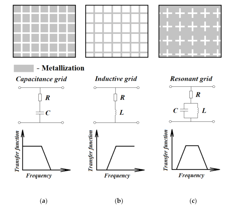
Cryogenic band-pass filters are required for the suppression of background IR radiation by three orders of magnitude to avoid the overheating of bolometers from radiation through the optical window. Such filters should have minimum losses at the signal frequency. Filters can be designed in the form of a periodic metal film frequency-selective surface (FSS). A period of the grid and size of a unit cell determines the resonant wavelength and beam pattern of the grid. The characteristics of the filters can be described by out-of-phase interference in the plane of the filter and in-phase interference normal to the surface of the filter. The distance between the adjacent elements is close to half a wavelength. For band-pass filters, inductive grids with cross-shaped openings are often used to obtain a higher Q-factor compared to square- and circle-shaped openings. An inductive grid is presented by electrically connected unit cells, as in Figure 1. In the simplest approximation, the openings in the unit cells can be viewed as diaphragms in the waveguide and described as parallel LC tank circuits inserted in the transmission line with an impedance equal to free space impedance, Z0. Such a description is valid for a single-mode waveguide. For resistive losses in such a circuit, both the resistivity of the metal and skin depth should be taken into account. For good conductors such as copper and gold, this resistance is much lower compared to Z0 at low temperatures, and the quality factor is determined by the ratio Z0/ω0L, that is, practically independent of R.
3.1. Thin-Film Filters
Metal film filters can be fabricated by various fabrication methods: evaporation, sputtering, etching, or lifting-off. Advanced designs are multilayer structures, as in [21,22]. For frequencies below 1 THz, such filters can be made of free-standing thin metal foil instead of thin film on a dielectric substrate.
We fabricated a series of band-pass filters for the central frequencies of 300, 450, 600, and 750 GHz [23]. Such filters were fabricated with chemical etching of 50 µm of thick copper foil, 20 µm of thick aluminum foil, chemical etching of copper-plated Teflon (35 µm of copper on 800 µm of Teflon carrier), and chemical etching of aluminum-plated Kapton. The shape of the openings was transferred to an S1813 photoresist from a photomask (Figure 2a) with dimensions ratios of period:length:width as P:L:W = 10:8:1. To avoid oxidation, copper foil was electrolytically gold plated. A photo of such a filter is presented in Figure 2b. The copper filters were etched in a solution of hydrogen peroxide and salt acid, and the aluminum was etched in orthophosphoric acid or in potassium hydroxide. Such filters were modeled in the CST STUDIO SUITE with Floquet ports and “unit cell” boundary conditions. Schematic images of some modeled filters are presented in Figure 3.
The spectral characteristics were measured with a BWO transmission spectrometer, a Fourier spectrometer (BECKMAN IR-720M), and an IR spectrophotometer (Shimadzu IR-460). At lower frequencies, better characteristics were obtained for copper foil filters, and at higher frequencies for thin-film filters evaporated on Mylar or Kapton. The best transmission losses were as low as −0.13 dB. The losses in the cascade of four filters was –0.9 dB. The cascade of four filters separated by filter paper was −1.5 dB. The fine alignment and tuning of the cascade filter can improve the Q-factor. Filters on thick Teflon inserted additional losses of about 1 dB due to the reflections from two air-Teflon boundaries. Filters made of 0.4 µm of aluminum on Kapton have additional losses of 5 dB that can be attributed to resistive losses in the thin aluminum film on top of an adhesion layer of 5 nm chromium. Furthermore, using the IR spectrophotometer, we measured the transmission of the filters in the IR band. Losses in this region are over 10 dB. The results of the measurements of the different filters in the frequency band 100–600 GHz are presented in Figure 4.
The out-of-band attenuation in a single filter at infrared (Figure 5) was above −11 dB in the wave range 2–20 μm; that is, more than the geometrical factor equal to the area of etched-away opening to the area of unit cell equals, which is −8.2 dB.
The operation of cryogenic bolometers is only possible at a strong suppression of the background IR radiation. For this purpose, special cold low-pass filters (for example, fluorogold) are used. The attenuation of the IR background by a band-pass filter outside its working band reduces the requirements for low-pass filters. The band-pass spectra of the grid filters in the 2.5- to 25-μm IR wavelength range are shown in Figure 5. Deep transmission minima at 6 and 13 μm relate to reflections and absorptions in the Mylar film, on which this filter is based. The filters can be efficiently staged in the IR wave range in contrast to the submillimeter range, since the mutual darkening of the holes of subsequent grids leads to the fact that the total transmission is much smaller than products of the transmissions of single filters. In our spectrometer, the signal transmitted through two filters was below the noise level, i.e., the attenuation exceeded 20 dB.
3.2. Capillary High-Pass Filters
High-pass filters can be fabricated similarly to thin-film band-pass filters. The thin-film metal mesh filters are available from industrial companies such as Virginia Diodes in the US and QMC in the UK. As with any thin-film mesh filters, they have some disadvantages, such as the Wood anomaly and losses at the edges due to the skin effect. The alternative solution is a waveguide filter. The properties of evanescent waveguides were studied in detail in [24]. The suppression of the long wavelength portion of radiation in this filter can be very high. Another important advantage of the evanescent waveguide as a filter is the sharpness of the transmission cutoff. In this case, the characteristics of the filters can be adjusted within wide limits by changing the diameters and lengths of the waveguides. The amplitude of the wave propagating in a waveguide is:
where Z is the coordinate along the waveguide, E is the intensity of the electric field at point Z, E0 is the intensity of the electric field at the initial point, and γ is the propagation constant, described as:
E(Z) = |E0|exp{iγZ}
γ = (2π/λcr) √(λcr/λ)2 − 1
If λ < λcr, we have an ordinary wave, but if λ > λcr, the propagation constant γ will be imaginary and the wave exponentially attenuates inside the waveguide.
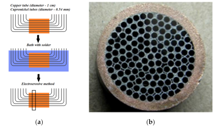
A single below-cutoff circular waveguide as a high-pass filter was experimentally studied in [24], and it obtained an attenuation of 6–12 dB in the passband and an attenuation of 30–60 dB in the stopband. Such a filter requires input and output horns and adapters if using in quasi-optical systems and makes construction rather complicated, large in size, and with non-uniform spectral characteristics. An array of capillaries can operate as a high-pass filter at millimeter and submillimeter waves without additional adapters. At lower frequencies, each capillary can be viewed as a below-cutoff circular waveguide. An array of capillaries does not need any adapters, it is relatively short, and can be inserted in any quasi-optical beam guide. Capillary arrays can be an alternative to perforated plates (grids) that need to be arranged as four to six parallel layers, and this pseudo high-pass filter is a band-pass filter with a bandwidth of about one octave [25]. Industrial manufacturers of multimesh terahertz filters, such as QMC Instruments (UK) and TYDEX (Russia), do not offer the high-performance high-pass filters that are required for cryogenic radiation sources intended for the calibration of superconducting bolometers. We fabricated a series of capillary array filters with different diameters and lengths of capillaries. The fabrication process consisted of the following steps: electroplating stainless or nickel–copper capillaries with Ni, filling short pieces of 10 mm inner diameter tube with as many capillaries as possible, soldering such packages with tin–lead alloy, electro-erosion cutting pieces of 1, 2, 3, and 4 mm long, and finally cleaning in an ultrasonic bath (Figure 6a). A photo of the fabricated capillary filter is presented in Figure 6b. The filters were placed in the waist of a quasi-optical beam guide comprising (Figure 7) a backward wave oscillator (BWO) radiation source, a corrugated horn, four Teflon lenses (focal length 20 cm and 40 cm), and a Goley cell detector. The transmission was measured in the frequency range 150–550 GHz. For an inner diameter of a capillary of 0.54 mm and a length of 3 mm, the attenuation of such a filter was over 40 dB at frequencies below 200 GHz. At frequencies above 350 GHz, attenuation does not exceed 5 dB. The results of the measurements are presented in Figure 8 and Figure 9.
As we mentioned above, our experimental curves are shifted to higher frequencies presumably due to slight pressing capillaries in fabrication process and some deformation. Squeezing capillary diameter in fabrication leads to reducing effective diameter in the middle and increasing of the cut-off frequency.
3.3. Cryogenic Tunable Filter-Interferometer of Fabry–Perot Type with Grid Meshes below 1/8 Wavelength Period
For developing a cryogenic measuring system and performing spectral measurements, it is very appealing to use a broadband calibrated cryogenic thermal radiation source combined with a tunable high-Q filter inside the cryostat. This solution makes it possible to significantly simplify the optical path in comparison with the use of a BWO source and a set of lenses at room temperature, as well as to remove multiple reflections and irregularities arising on the optical windows of the cryostat. As a tunable filter, a mesh filter of the Fabry–Perot interferometer type can be used [26]. One of the requirements for the implementation of such a design is a good reflectivity of the meshes. In our experiment, metal film grid filters on quartz substrates were used as meshes (interferometer mirrors). A photo of the golden mesh is presented in Figure 10a. For a backlash-free tuning of distance between meshes, we fabricated a gadget with magnetic pushers made from SmCo magnetic rods. The mandrels were facing each other with the same poles, so that pushing the mandrels back and forth was smooth, without sticking or backlash. For photos of the mechanical parts of such a tunable interferometer, see Figure 10b. The assembled tunable filter consisted of two metal film meshes on quartz substrates that could be pushed apart by the rotation of ring diaphragms in the M50 × 0.75 screw. One complete revolution of the mesh ring corresponded to a movement of 0.75 mm. The initial gap between the meshes was 0.1 mm. The meshes were oriented facing the metallic film sides and dielectrics oriented outside. The transmission of one such grid in the 500 GHz band was below 4%, which fulfills the requirements of interferometer meshes.
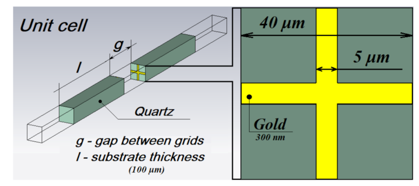
The frequency response of such a filter tuned to a frequency of 300 GHz was calculated. The calculation was carried out in the following configuration: the grids on the substrates faced each other, the distance between the grids was 500 μm, which corresponded to half the wavelength at a given frequency. Optical quartz for the substrate and gold for the grating material were chosen as reference materials for numerical simulations. This periodic lattice was simulated for the characteristic cell dimensions with periodic boundary conditions. The cross size was 40 μm, width was 5 μm, film thickness was 0.3 μm, and substrate thickness was 240 μm. The simulation projects were calculated both in CST STUDIO SUITE and HFSS programs (see a view of the model in Figure 11). The calculated transmission spectral results are presented in Figure 12 in the frequency range 100–1000 GHz. The main resonant transmission feature was present at a frequency of approximately 300 GHz and harmonics at 600 and 900 GHz. A slight downshift of maxima from the expected frequency was related to the so-called “sagging electric field” effect in the grids and is more pronounced at higher frequencies. For the first version of the filter, the grids were made of gold on quartz substrates with a thickness of 240 μm, a diameter of 25 mm, a gold thickness of 300 nm, a stripe width of 5 μm, and a period of 40 μm. The transmission was measured by the substitution method in a transmission BWO spectrometer. A holder with meshes was installed in a four-lens beam guide (Figure 7) in the waist of the formed Gaussian beam, where the wave front is the flattest. The results of the experimental study are shown in Figure 13a. In addition, the aluminum filter on the glass substrate was investigated (Figure 13b).
Such a filter was used to measure the response of the SINIS bolometer [27]. A “fast” blackbody radiation source on a sapphire substrate was used as the emitter, which made it possible to operate at a modulation frequency of 20 Hz. To move the meshes inside the cryostat, the design of a worm drive connected to the filter draft by a long shaft made of a thin-walled stainless tube was developed (see Figure 14). The operation of the filter was demonstrated with a SINIS bolometer mounted at the 273 mK stage in a helium-3 Heliox-AC-V sorption cryostat. Reduced and broadened spectrum for black body source is due to broad illumination angle for such wide aperture and corresponding different resonant distances for different angles of incidence. Similar to [28], the Fabry–Perot resonance is dependent on incidence and polarization angles. With our black-body radiation source placed close to interferometer, these angles vary from normal to meshes to about ϕ = 30° from normal. The corresponding resonant distance varies from actual distance d for normal incidence to d/cosϕ and brings broadening of transmission spectrum by about 15%.
3.4. Methods of FSS Modeling
Alternative methods for FSS modeling can be applied in CST STUDIO SUITE, HFSS, and Mathcad projects. One approach is using Floquet’s theorem with the unit cell in the infinite matrix, assuming the electromagnetic field in each cell can differ only by a complex multiple. Another approach is modeling the whole array with all complex interactions between elements.
A Floquet cell is a space element limited on the sides by periodic boundary conditions, with the radiation source presented by a plane wave emerging at coordinate Zmax (schematic model in Figure 15). Electric field E (and similar for magnetic field H) for a Floquet port can be presented, similar to [28], as:
where an,m are the amplitudes of n, m harmonics; k is the wave number for free space; kn = k0 + 2πn/Lx; βm = β0 + 2πm/Ly; γn,m = √(k2 − kn2 − βm2); k0, β0 are determined by the applied field, which is presented by a plane wave; and Lx,y are the repetition periods for axes OX and OY. Incident field is plane wave k0 = k·sinθ·cosϕ, θ is inclination angle, and ϕ is azimuth angle.
E(x,y,z) = ∑n∑m an,m∙exp{−iknx − iβmy − γn,mz}
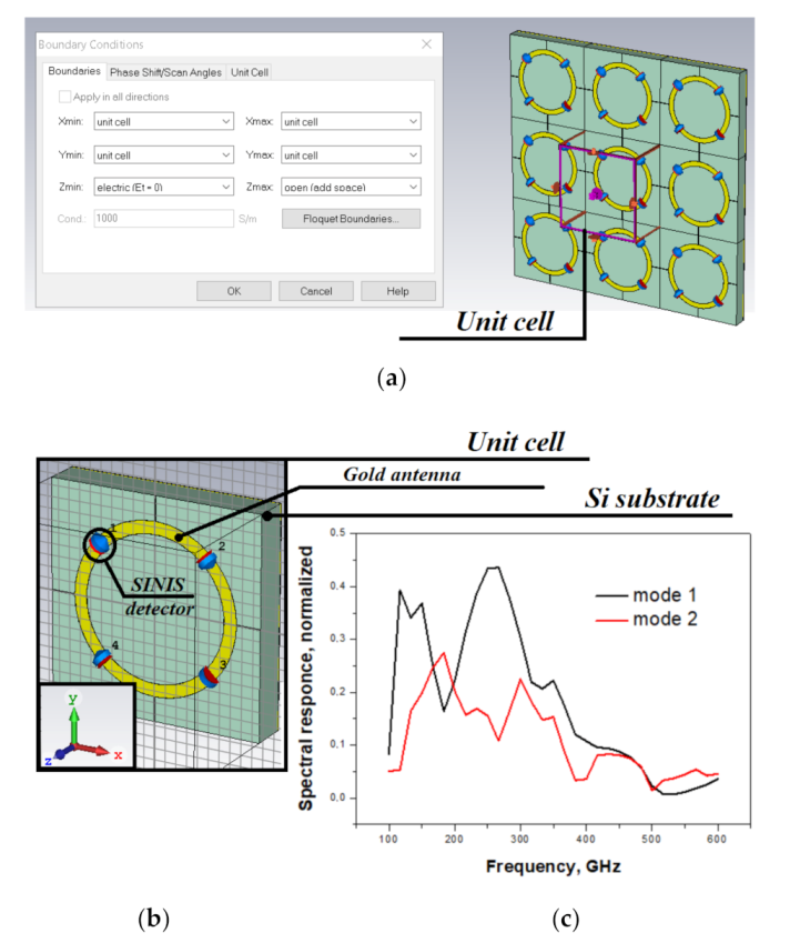
Such a method allows us to quickly obtain rough estimations of any periodic structure, and is widely used for the simulation of periodic quasi-optical filters. For the simulation of detector arrays, such a method can provide only approximate results, because the dissipation makes phases of reflected and re-illuminated signals uncertain. For nondissipative case the lateral sides of the unit cell were allocated a Floquet periodicity conditions with a wave vector resulting from the calculated values of the wave vector within one cell. Absorption in each unit cell is independent and phases of wave vectors are indefinite, the mutual influence of the elements with actual phases is not accounted for. In Figure 15, the single-cell approach according to Floquet’s theorem is presented. For comparison, the results of the modeling of the whole array of conventional half-wave antennas with SINIS detectors are presented in Figure 16 (the results of modeling from [29]). Here, we should mention that such a technique is suitable for the modeling of phased antenna arrays.
By scaling the dimensions of an FSS, it is easy to obtain arrays for different spectral bands. The modeling and scaling of circular antennas for the central frequencies of 90, 150, 230, 350, and 480 GHz, and photos of fabricated samples are presented in [14] and in Figure 17, with experimental results at 95 and 350 GHz.
4. Transition from Arrays of Half-Wave Antennas to Arrays of Electrically Small Antennas with SINIS Detectors
4.1. Numerical Modeling and Simulation Algorithm
A high background power load can saturate a single bolometer. For a SINIS bolometer, the typical saturation power level is 1 pW. To increase the dynamic range of ground-based receivers, single elements are integrated in arrays, and the incoming power is distributed between many elements. Unit antenna cells can be of different types and parameters depending on the requirements for selectivity, polarization, beam pattern, etc. In our case, the most suitable is an annular ring antenna (for details, see [14,23]). An ordinary annular ring antenna resonant wavelength corresponds to its perimeter. As an example, an antenna for 345 GHz has a resonant wavelength of 0.87 mm in a vacuum and 0.26 mm on a silicon substrate. The radius of such an antenna without additional reactance elements on a Si substrate is 0.138 mm.
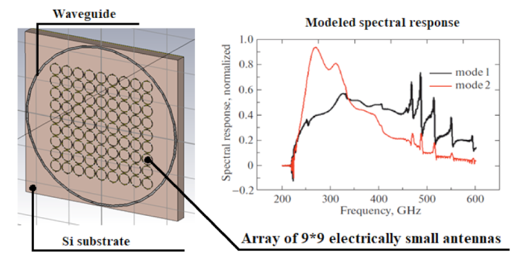
A square array of 5 × 5 elements is depicted in Figure 16 and Figure 17 (left). A feeding port for an illuminating array was inserted in a circular waveguide 10 mm long and 3 mm in diameter. The two polarizations were marked as mode 1 (along connection lines) and mode 2 (across connection lines) for the first circular waveguide mode E01. The difference in spectral response for the two orthogonal polarizations was determined by the interconnection elements placed along the electric field direction for mode 2. The measurement results in the main 350 GHz frequency band are presented in Section 3.3. Furthermore, we also tested the signal response at the much lower frequency of 90 GHz, which demonstrated rather effective receiving. This experiment led to the conclusion to use the configuration of electrically small antennas much less in diameter compared to half wavelengths (about λ/10). We reduced the antenna diameter from 300 μm to 54 µm for the new array comprising 9x9 antennas (see Figure 18). As a result, on the smaller area, we were able to integrate more detecting elements and to increase the saturation power for the same focal plane area. An initial simplified estimation for a unit cell in an infinite matrix with periodic boundary conditions was presented in [5,15]. It results in a rough estimation, but it does not reflect the fine spectral features of arrays of incoherent receiving elements. For the exact spectral simulation, we developed a full model array of 9 × 9 elements with 324 ports (Figure 18, left). The spectral response for the two polarizations are presented in Figure 18 (right). A sharp decrease below 220 GHz is determined by the cutoff frequency of the feeding waveguide. This corresponds to the actual configuration of our experimental setup [29,30]. The obtained spectral dependence is more complicated compared with the unit cell model with Floquet ports, and corresponds more closely to the experimental results. Such arrays of electrically small antennas are equivalent to a distributed absorber that absorbs radiation in a wide frequency range. For comparison, we also simulated six different shapes of annular antennas (see Table 1 and Table 2 and Figure 19).
4.2. Fabrication Technologies
The fabrication process can be divided into two stages: the first is shaping the FSS, wiring and contact pads, and the second stage is the fabrication of the SINIS detectors. The technology of the normal metal-insulator-superconductor (NIS) tunnel junctions is described in detail in our review article [31], and in this section, we present some specific features of these fabrication recipes.
The first layer with FSS can be fabricated using a lift-off process. After cleaning, the substrate is spin-covered with double-layer or inversed photoresist and baked. The resist is exposed by a laser or e-beam lithographer and developed. A thin film of FSS material (usually 10 nm Ti/100 nm Au/20 nm Pd) is deposited by thermal evaporation, e-beam evaporation, or magnetron sputtering. The first Ti layer improves the adhesion to the substrate, the second Au layer is low-loss material for the antenna, and the third Pd buffer layer is intended to reduce the resistance between the Au and the aluminum electrodes of the detector. The first three-layer sandwich fabrication process is schematically presented in Figure 20.
The second stage is the fabrication of SINIS detectors (see the schematic in Figure 21). The incoming radiation is absorbed by a thin film of normal (non-superconducting) metal. The temperature variation of the absorber is measured by tunnel NIS junctions connected to the edges of the absorber. High-quality tunnel junctions can be fabricated in one vacuum cycle using the shadow evaporation technique. One method is the Dolan technique with a suspended bridge of resist [32], another is the so-called bridge-free technique with evaporation into orthogonal grooves [33]. Later, we developed a process with magnetron sputtering, two lithography steps, and reactive ion etching [34]. Furthermore, we also developed a novel process of suspended bolometer fabrication (see Figure 21d). A detailed description of the recipes is presented in [31], and photos, in Figure 22.
4.3. Experimental Studies and Comparison with Modeling
The spectral evaluation of the fabricated samples is based on backward-wave oscillator (BWO) radiation sources. Four such sources cover the frequency range 70–600 GHz. The output power spectrum of the BWO is rather non-uniform and requires a broadband detector for monitoring and calibration. Moreover, on the way from the BWO to the sample, the probe signal is attenuated and reflected from cryostat windows, filters, a sample holder, and elements of the beam guide. For the correct spectral measurements, an experimental setup was equipped with three calibration channels. First, with the pyroelectric detector close to the BWO, an estimation of the BWO and output horn spectrum is provided. Second, the channel with the RuOx bolometer provides a measurement of the power approaching the sample holder. The third one, comprising an array of NIS junctions, monitors the power approaching the chip with the bolometer under test. Such a complicated calibration technique is described in detail in [29]. A schematic view of the experimental setup is presented in Figure 23. Measured spectra of arrays of half-wave and electrically small antennas are presented in Figure 24.
5. Discussion
The creation of receiving matrices and filtering elements in the MM and subMM wave ranges is one of the most in-demand tasks today, as such structures can be applied in various fields from radio astronomy research to the creation of scanning matrices for security systems. The methodology for modeling, manufacturing, and measuring such devices has become relevant. Matrices based on half-wave unit cells are the most popular building blocks. To create a broadband receiving structure, it is important to develop electrically small antennas with a characteristic element size λ/10 or less—an analogue of a distributed absorber. With an increase in the frequency range and a decrease in the size of single elements and the period, the calculation of the characteristics of such structures becomes a complex computational problem. A modern approach is numerical simulation in software packages such as CST STUDIO SUITE and HFSS. However, the results obtained by the numerical simulation method do not always reflect the real (or close to real) electrodynamic picture of the matrices being developed. In the pursuit of a decrease in computing power and a reduction in computation time, a modeling technique is used with Floquet ports, infinite matrices, and periodic unit cell boundary conditions. The condition that the electromagnetic field in a single cell differs only by a complex component can be applicable only for the case of phased antenna arrays, or filtering devices in the absence of dissipation. In the case of antenna arrays with integrated SINIS detectors, we observe a more complex electrodynamic picture. This is especially important for receiving matrices consisting of electrically small elements, since in this case, the mutual influence of the adjacent elements on each other is significant, which is not taken into account when calculating the unit cell. As an example, Figure 25 shows the simulated spectral responses of the matrices of electrically small antennas using two methods: a single cell with Floquet ports and an entire matrix consisting of 81 ring antennas, each of which is integrated with four SINIS detectors.
As noted above, the simplified method for calculating a unit cell is quite applicable for studying the characteristics of filters based on periodic structures. The difference between the calculated and experimental results of the study (a small shift in frequency and bandwidth) of filtering devices (Figure 4, Figure 8, Figure 9 and Figure 13) is due to the following: the imperfect size and shape of the fabricated structures and the difference in the basic characteristics (mainly dielectric constant) used in the substrate materials in a practical and simulated case. Considering the results of modeling filters on thick substrates (quartz 100 µm and Teflon 800 µm, Figure 4a), “parasitic resonances” can be explained by the fact that the resonance of the etched structures (crosses) is combined with the Fabri–Perot resonance on a plane-parallel plate.
The evaluation and comparison of the theoretical and experimental characteristics of receiving matrices with integrated superconducting detectors, in contrast to filtering devices, is a more difficult task, as on the path “source-receiver”, there are multiple reflections both on the windows of the cryostat and inside it that will require huge computing power and supercomputers to simulate. In addition, it should be noted that the power level of the signal source (in our case, the backward wave oscillator) is significantly nonuniform. To take into account multiple reflections when measuring the characteristics of such receiving structures and refining the shape of the spectral response, it is possible to introduce additional reference channels to calibrate the received signal, as was done in [29] (see Figure 23).
Active receiving and passive filtering matrices have some common features. In both cases, we have two scale approaches: half wavelength and electrically small unit cells. The first case corresponds to frequency-selective surface (FSS), and the second to the distributed absorber model. For passive filters with low losses, modeling can be simplified using a unit cell and periodic boundary conditions. Detector arrays with absorbers require a full model of arrays that account for the interaction between a finite number of elements.
6. Conclusions
The numerical modeling, development, fabrication, and an experimental study of a family of matrices of cryogenic metamaterials in the form of periodic structures of passive and active elements of a quasi-optical receiver (band-pass filters, grid interferometers, distributed absorbers, and frequency-selective surfaces with planar antennas and integrated SINIS bolometers) was carried out. We used two alternative approaches to the calculation of such periodic structures: the numerical model of a single cell with periodic boundary conditions for passive reactive cells; and the calculation of the complete structure with hundreds of independent active absorbing ports for arrays of bolometers. Structures with half-wave unit cells are suitable for narrow-band applications, and matrices with electrically small unit cells are advantageous for broad-bang applications.
7. Patents
- M. Tarasov, A. Gunbina, D. Nagirnaya, and M. Fominsky, Method of making device with thin-film tunnel junctions, Patent RU2733330C1, Russia, 2019.
- M. Tarasov, A. Gunbina, A. Chekushkin, and M. Fominsky, Method of fabrication of thin-film tunnel junctions by means of separate lithography, application for patent, № No 2021108441 RU 30 March 2021.
Author Contributions
Conceptualization, M.T. and V.V.; methodology, A.K.; design, M.T., A.G. and A.C.; simulation, A.G.; fabrication, A.G.; microwave experiment, A.C. and A.G.; writing—original draft preparation, M.T.; writing—review and editing, A.K. All authors have read and agreed to the published version of the manuscript.
Funding
This research was funded by the Russian Science Foundation, grant number 21-42-04421. Equipment from USU “Cryointegral” was used to carry out the research; USU is supported by a grant from the Ministry of Science and Higher Education of the Russian Federation, agreement No. 075-15-2021-990.
Institutional Review Board Statement
Not applicable.
Informed Consent Statement
Not applicable.
Data Availability Statement
Not applicable.
Conflicts of Interest
The authors declare no conflict of interest.
References
- Day, P.; LeDuc, H.G.; Dowell, C.D.; Lee, R.A.; Turner, A.; Zmuidzinas, J. Distributed antenna-coupled TES for FIR detector arrays. J. Low Temp. Phys. 2008, 151, 477–482. [Google Scholar] [CrossRef]
- Day, P.K.; LeDuc, H.G.; Mazin, B.A.; Vayonakis, A.; Zmuidzinas, J. A broadband superconducting detector suitable for use in large arrays. Nature 2003, 425, 817–821. [Google Scholar] [CrossRef]
- Paiella, A.; Ade, P.A.R.; Battistelli, E.S.; Castellano, M.G.; Colantoni, I.; Columbro, F.; Coppolecchia, A.; D’Alessandro, G.; de Bernardis, P.; De Petris, M.; et al. In Flight Performance of the LEKIDs of the OLIMPO Experiment. J. Low Temp. Phys. 2020, 199, 491–501. [Google Scholar] [CrossRef] [Green Version]
- Tarasov, M.; Gunbina, A.; Yusupov, R.; Chekushkin, A.; Nagirnaya, D.; Lemzyakov, S.; Vdovin, V.; Edelman, V.; Kalaboukhov, A.; Winkler, D. Non-thermal absorption and quantum efficiency of SINIS bolometer. IEEE Trans. Appl. Supercond. 2021, 31, 2300105. [Google Scholar] [CrossRef]
- Tarasov, M.; Sobolev, A.; Gunbina, A.; Yakopov, G.; Chekushkin, A.; Yusupov, R.; Lemzyakov, S.; Vdovin, V.; Edelman, V. Annular antenna array metamaterial with SINIS bolometers. J. Appl. Phys. 2019, 125, 174501-1–174501-6. [Google Scholar] [CrossRef]
- Tarasov, M.A.; Gunbina, A.A.; Mahashabde, S.; Yusupov, R.A.; Chekushkin, A.M.; Nagirnaya, D.V.; Edelman, V.S.; Yakopov, G.V.; Vdovin, V.F. Arrays of annular antennas with SINIS bolometers. IEEE Trans. Appl. Supercond. 2020, 30, 2300106. [Google Scholar] [CrossRef]
- Veselago, V.G. Electrodynamics of materials with negative index of refraction. J. Phys. Uspekhi 2003, 46, 764–768. [Google Scholar] [CrossRef]
- Munk, B.A. Frequency Selective Surfaces: Theory and Design; John Wiley & Sons: New York, NY, USA, 2005. [Google Scholar]
- Danila, O. Polyvinylidene fluoride-based metasurface for high-quality active switching and spectrum shaping in the Terahertz G-band. Polymers 2021, 13, 1860. [Google Scholar] [CrossRef] [PubMed]
- Danila, O. Spectroscopic assessment of a simple hybrid si-Au cell metasurface-based sensor in the mid-infrared domain. J. Quant. Spectrosc. Radiat. Transf. 2020, 254, 107209. [Google Scholar] [CrossRef]
- Danila, O.; Manaila-Maximean, D.; Barbar, A.; Loiki, V. Non-layered gold-silicon and all-silicon frequency-selective metasurfaces for potential mid-infrared sensing applications. Sensors 2021, 21, 5600. [Google Scholar] [CrossRef]
- Varikuntla, K.K.; Singaravelu, R. Design of a novel 2.5D frequency selective surface element using Fibonacci spiral for radome application. In Proceedings of the 2018 Asia-Pacific Microwave Conference (APMC), Kyoto, Japan, 6–9 November 2018; 2019. [Google Scholar] [CrossRef]
- Zhao, Z.; Li, W.; Yang, Y.; Huo, H.; Li, J.; Zhang, A. An incident angle insensitive band-pass frequency selective surface with flat top. In Proceedings of the 2017 IEEE International Symposium on Antennas and Propagation & USNC/URSI National Radio Science Meeting IEEE, San Diego, CA, USA, 9–14 July 2017; pp. 273–274. [Google Scholar] [CrossRef]
- Mahashabde, S. Frequency Selective Cold-Electron Bolometer Arrays. Ph.D. Thesis, Chalmers University of Technology, Gothenburg, Sweden, 2015. [Google Scholar]
- Sobolev, A.S.; Beiranvand, B.; Chekushkin, A.M.; Kudryashov, A.V.; Tarasov, M.A.; Yusupov, R.A.; Gunbina, A.; Vdovin, V.F.; Edelman, V. Wideband metamaterial-based array of SINIS bolometers. In Proceedings of the 3rd International Conference “Terahertz and Microwave Radiation: Generation, Detection and Applications” (TERA-2018), EPJ Web of Conferences, Nizhny Novgorod, Russia, 22–25 October 2018; Volume 195, p. 05009. [Google Scholar] [CrossRef] [Green Version]
- Chase, S.T.; Joseph, R.D. Resonant array bandpass filters for far infrared. Appl. Opt. 1983, 22, 1775–1779. [Google Scholar] [CrossRef]
- Melo, A.M.; Gobbi, A.L.; Piazzetta, M.H.O.; da Silva, A.M.P.A. Cross-shaped Terahertz metal mesh filters: Historical review and results. Adv. Opt. Technol. 2012, 2012, 530512. [Google Scholar] [CrossRef]
- Ferraro, A.; Zografopoulos, D.C.; Caputo, R.; Beccherelli, R. Angle-resolved and polarization-dependent investigation of cross-shaped frequency-selective surface terahertz filters. Appl. Phys. Lett. 2017, 110, 141107. [Google Scholar] [CrossRef]
- Porterfield, D.W.; Hesler, J.L.; Densing, R.; Mueller, E.R.; Crowe, T.W.; Weikle, R.M. Resonant metal-mesh bandpass filters for the far infrared. Appl. Opt. 1994, 33, 6046–6052. [Google Scholar] [CrossRef]
- Ferraro, A.; Tanga, A.A.; Zografopoulos, D.C.; Messina, G.C.; Ortolani, M.; Beccherelli, R. Guided mode resonance flat-top bandpass filter for terahertz telecom applications. Opt. Lett. 2019, 17, 4239–4242. [Google Scholar] [CrossRef] [PubMed]
- Pisano, G.; Ng, M.W.; Haynes, V.C.; Maffei, B. A broadband metal-mesh half-wave plate for millimeter wave linear polarisation rotation. Prog. Electromagn. Res. M 2016, 25, 101–114. [Google Scholar] [CrossRef] [Green Version]
- Rahim, T.; Khan, F.A.; Jiadong, X. Design of X-band Frequency Selective Surface (FSS) with band pass characteristics based on miniaturized unit cell. In Proceedings of the 2016 13th International Bhurban Conference on Applied Sciences and Technology (IBCAST), Islamabad, Pakistan, 12–16 January 2016. [Google Scholar]
- Tarasov, M.A.; Gromov, V.D.; Bogomolov, G.D.; Otto, E.A.; Kuzmin, L.S. Fabrication and characteristics of mesh band-pass filters. Instrum. Exp. Tech. 2009, 52, 74–78. [Google Scholar] [CrossRef]
- Syzranov, V.S.; Ermolov, A.S.; Lebedev, S.P.; Murzin, V.N. Design and studying waveguide filters of terahertz and sub-terahertz frequency ranges. Instrum. Exp. Tech. 2012, 55, 673–679. [Google Scholar] [CrossRef]
- Ulrich, R. Interference filters for far infrared. Appl. Opt. 1986, 7, 1987–1996. [Google Scholar] [CrossRef] [PubMed]
- Chekushkin, A.M.; Yusupov, R.A.; Zavyalov, V.V.; Kuzmin, L.S.; Tarasov, M.A. Cryogenic tunable spectral filter for the calibration of highly sensitive bolometers. J. Radioelectron. 2017, 1–8. [Google Scholar]
- Tarasov, M.; Chekushkin, A.; Jonsson, L.; Kuzmin, L. Grid interferometer for spectral calibration of cryogenic bolometers. In Proceedings in the 14th International Workshop “High-Frequency Superconducting Electronics”, Björkliden, Kiruna, Sweden, 10–16 April 2016. [Google Scholar]
- Kurushin, A.A. Implementation of Fouquet Channels for Modelling of Periodic Nanostructure. 2010, p. 22. Available online: http://jre.cplire.ru/jre/nov10/5/text.html#4 (accessed on 2 October 2021).
- Gunbina, A.A.; Tarasov, M.A.; Lemzyakov, S.A.; Chekushkin, A.M.; Yusupov, R.A.; Nagirnaya, D.V.; Mansfel’d, M.A.; Vdovin, V.F.; Winkler, D.; Kalaboukhov, A.S.; et al. Spectral response of arrays of half-wave and electrically small antennas with SINIS bolometers. Phys. Solid State 2020, 62, 1504–1611. [Google Scholar] [CrossRef]
- Tarasov, M.A.; Chekushkin, A.M.; Yusupov, R.A.; Gunbina, A.A.; Edelman, V.S. Matching of radiation with array of planar antennas with SINIS bolometers in an integrating cavity. J. Commun. Technol. Electron. 2020, 65, 60–68. [Google Scholar] [CrossRef]
- Gunbina, A.A.; Tarasov, M.A.; Fominsky, M.Y.; Chekushkin, A.M.; Yusupov , R.A.; Nagirnaya, D.V. Fabrication of aluminium nanostructures for microwave detectors based on tunnel junctions. In Book Advances in Microelectronics: Reviews; Sergey, Y.Y., Ed.; IFSA Publishing, S.L.: Barcelona, Spain, 2021; Volume 3, pp. 183–212. [Google Scholar]
- Dolan, G.J. Offset masks for lift-off photoprocessing. Appl. Phys. Lett. 1977, 31, 337–339. [Google Scholar] [CrossRef]
- Tarasov, M.; Gunbina, A.; D. Nagirnaya, D.; Fominsky, M. Method of Making Device with Thin-Film Tunnel Junctions. Patent RU2733330C1, 1 October 2020. [Google Scholar]
- Tarasov, M.; Gunbina, A.; Chekushkin, A.; Fominsky, M. Method of Fabrication of Thin-Film Tunnel Junctions by Means of Separate Lithography. Patent NO. 2021108441 RU, 22 September 2021. [Google Scholar]
Figure 1.
Basic frequency-selective surfaces: (a) capacitive mesh; (b) inductive mesh; and (c) combined (resonant) mesh. Grey color—metal film, white—openings.
Figure 1.
Basic frequency-selective surfaces: (a) capacitive mesh; (b) inductive mesh; and (c) combined (resonant) mesh. Grey color—metal film, white—openings.

Figure 2.
(a) Unit cell and (b) photo of fabricated 600 GHz filter with 625 μm period.

Figure 3.
Schematic image of modeled structure: (a) foil filters; and (b) copper filter on Mylar substrate.
Figure 3.
Schematic image of modeled structure: (a) foil filters; and (b) copper filter on Mylar substrate.

Figure 4.
Transmission spectra for different filters: (a) numerical modeling of copper filters on thick substrates (quartz 100 µm and Teflon 800 µm); (b) Au thin film filters: calculations and measurements; (c) comparison of calculated and measured results in narrow band for Al and Cu foil filters; (d) calculation and measurements of Cu filter on Mylar substrate; (e) calculation and measurements of Cu filter on Kapton; and (f) calculation and measurements of Cu filter on quartz. Frequency downshift is due to the difference of characteristics in the real and modeled dielectric substrate.


Figure 5.
The results of measurements of Al foil filter (1) and Al filter on Mylar substrate (2). Measurements from [23].
Figure 5.
The results of measurements of Al foil filter (1) and Al filter on Mylar substrate (2). Measurements from [23].

Figure 6.
Capillarity filter: (a) fabrication process; and (b) photo of capillary filter.

Figure 7.
Photo and schematic view of experimental setup for filter evaluation: 1—BWO, 2, 4—lenses, 3—chopper, 5—filter under test, and 6—pyroelectric detector.
Figure 7.
Photo and schematic view of experimental setup for filter evaluation: 1—BWO, 2, 4—lenses, 3—chopper, 5—filter under test, and 6—pyroelectric detector.

Figure 8.
Investigation of capillary filter 200 and 350 GHz band: (a) schematic image of modeled structure; and (b) results of numerical modeling and experimental tests. Experimental curves are shifted to higher frequencies presumably due to slight pressing capillaries in the fabrication process and deformation.

Figure 9.
Investigation of dependence of filter’s characteristic on capillary length: (a) the results of modeling; and (b) the results of measurements of thick (4 mm long) and thin (2 mm long) filters.
Figure 9.
Investigation of dependence of filter’s characteristic on capillary length: (a) the results of modeling; and (b) the results of measurements of thick (4 mm long) and thin (2 mm long) filters.


Figure 10.
Tunable interferometer: (a) golden mesh evaporated on quartz substrate; (b) mechanical parts of the gadget; and (c) assembled interferometer.
Figure 10.
Tunable interferometer: (a) golden mesh evaporated on quartz substrate; (b) mechanical parts of the gadget; and (c) assembled interferometer.

Figure 11.
Design view of unit cell for numerical modeling.

Figure 12.
Calculated dependence of the interferometer transmission spectrum for 4 distances between meshes.
Figure 12.
Calculated dependence of the interferometer transmission spectrum for 4 distances between meshes.

Figure 13.
Results of the theoretical and experimental study of the transmission of an interferometer depending on the distance between the grids: (a) measurements of a gold filter on a quartz substrate from the radiation source of the avalanche diode at 232 GHz (red) and 95 GHz (blue); and (b) measurements of an aluminum filter on a glass substrate carried out by changing the distance between the filter grids.

Figure 14.
(a) Blackbody radiation source, tunable filter at 3 K stage, and bolometer under test at 273 mK temperature stage; and (b) response measured with blackbody source (red) and 232 GHz IMPATT source (black). Reduced and broadened spectrum for black body source is due to broad illumination angle for such wide aperture and corresponding different resonant distances for different angles of incidence.

Figure 15.
Modeling of half-wave antenna array using Floquet’s theorem in CST STUDIO SUITE. (a) Boundary conditions; (b) unit cell of the investigated structure antenna is made of gold with four integrated SINIS detectors on the Si substrate. On the back side of the substrate, a 1 µm film of an Au counter-reflector is deposited (Zmin–electrical boundary conditions). The source is a plane wave emerging at the boundary Zmax (c).

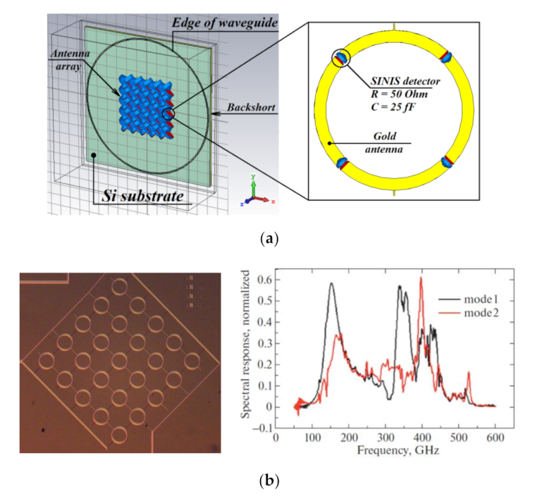
Figure 16.
Results of modeling of the whole array of 25 annular antennas as in Figure 2: (a) schematic image of modeled structure with description; and (b) optical image of fabricated array (left) and results of modeling for two polarization modes, along connection lines (mode 1) and across (mode 2), as in [22].

Figure 17.
(a) Simulated spectral response (lines), experiment (circles) of different half-wave antennas arrays from; (b) SEM image of 350 GHz array; (c) Photo of 240 GHz array in sample holder; and (d) photo of 90 GHz array in sample holder. Results and photos from [14].
Figure 17.
(a) Simulated spectral response (lines), experiment (circles) of different half-wave antennas arrays from; (b) SEM image of 350 GHz array; (c) Photo of 240 GHz array in sample holder; and (d) photo of 90 GHz array in sample holder. Results and photos from [14].

Figure 18.
Model of 9 × 9 array of small antennas (left) and calculated spectral response (right).

Figure 19.
Spectral response calculated for six different matrices of electrically small antennas: (a) Mode 1; (b) Mode 2. Number labels are the same as in Table 1.
Figure 19.
Spectral response calculated for six different matrices of electrically small antennas: (a) Mode 1; (b) Mode 2. Number labels are the same as in Table 1.

Figure 20.
Schematic of the first three-layer fabrication process: (a) profile of inversed and (b) double-layer positive resists, and deposited films underneath; (c) optical image of developed resist; and (d) deposited Ti/Au/Pd film comprising annular antenna and wiring.
Figure 20.
Schematic of the first three-layer fabrication process: (a) profile of inversed and (b) double-layer positive resists, and deposited films underneath; (c) optical image of developed resist; and (d) deposited Ti/Au/Pd film comprising annular antenna and wiring.

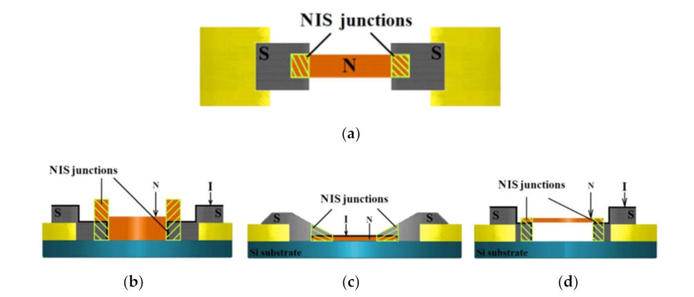
Figure 21.
Schematic view of SINIS detector from [15]: (a) top view; (b–d) cross-section of three SINIS types: thick absorber deposited as last layer (b), thin absorber deposited first (c), and suspended absorber (d).
Figure 21.
Schematic view of SINIS detector from [15]: (a) top view; (b–d) cross-section of three SINIS types: thick absorber deposited as last layer (b), thin absorber deposited first (c), and suspended absorber (d).

Figure 22.
SEM images of detectors fabricated by: (a) Dolan technique of shadow evaporation; (b) bridge-free shadow evaporation; and (c) suspended absorber (see also [31]).
Figure 22.
SEM images of detectors fabricated by: (a) Dolan technique of shadow evaporation; (b) bridge-free shadow evaporation; and (c) suspended absorber (see also [31]).

Figure 23.
Experimental setup for spectral evaluation of cryogenic detectors comprising cryostat with optical windows, filters, calibration detectors, BWO source, chopper, and pyroelectric detector [29].
Figure 23.
Experimental setup for spectral evaluation of cryogenic detectors comprising cryostat with optical windows, filters, calibration detectors, BWO source, chopper, and pyroelectric detector [29].

Figure 24.
Measured spectral response of arrays of half-wave (a) and electrically small (b) antennas from [29], black as it is from detector voltage response, and red after corrections from the reference channel (not averaging).
Figure 24.
Measured spectral response of arrays of half-wave (a) and electrically small (b) antennas from [29], black as it is from detector voltage response, and red after corrections from the reference channel (not averaging).

Figure 25.
The calculated spectral response of matrices of electrically small antennas using two methods: (a) a single cell with Floquet ports; and (b) an entire matrix modeling [5,15,22].


Table 1.
Parameters of six types of electrically small antennas.
| Array # | 1 | 2 | 3 | 4 | 5 | 6 |
|---|---|---|---|---|---|---|
| Parameter, μm | ||||||
| Outer radius | 33 | 33 | 33 | 33 | 33 | 50 |
| Inner radius | 30 | 30 | 3 | 15 | 30 | 3 |
| Connecting wire | 4 | 29 | 29 | 29 | 8 | 3 |
| Period | 70 | 95 | 95 | 95 | 74 | 103 |
Table 2.
Image of part of modeled structure number labels are the same as in Table 1.
Table 2.
Image of part of modeled structure number labels are the same as in Table 1.
| Array # | 1 | 2 | 3 |
|---|---|---|---|
 |  |  | |
| Array # | 4 | 5 | 6 |
 |  |  |
Publisher’s Note: MDPI stays neutral with regard to jurisdictional claims in published maps and institutional affiliations. |
© 2021 by the authors. Licensee MDPI, Basel, Switzerland. This article is an open access article distributed under the terms and conditions of the Creative Commons Attribution (CC BY) license (https://creativecommons.org/licenses/by/4.0/).
Share and Cite
MDPI and ACS Style
Tarasov, M.; Gunbina, A.; Chekushkin, A.; Vdovin, V.; Kalaboukhov, A. Arrays of Sub-Terahertz Cryogenic Metamaterial. Appl. Sci. 2021, 11, 9649. https://0-doi-org.brum.beds.ac.uk/10.3390/app11209649
AMA Style
Tarasov M, Gunbina A, Chekushkin A, Vdovin V, Kalaboukhov A. Arrays of Sub-Terahertz Cryogenic Metamaterial. Applied Sciences. 2021; 11(20):9649. https://0-doi-org.brum.beds.ac.uk/10.3390/app11209649
Chicago/Turabian StyleTarasov, Mikhail, Aleksandra Gunbina, Artem Chekushkin, Vyacheslav Vdovin, and Aleksei Kalaboukhov. 2021. "Arrays of Sub-Terahertz Cryogenic Metamaterial" Applied Sciences 11, no. 20: 9649. https://0-doi-org.brum.beds.ac.uk/10.3390/app11209649
Note that from the first issue of 2016, this journal uses article numbers instead of page numbers. See further details here.