
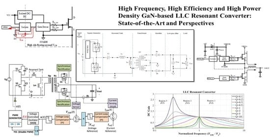
High Frequency, High Efficiency, and High Power Density GaN-Based LLC Resonant Converter: State-of-the-Art and Perspectives

 ,
,
Abstract
:
1. Introduction
2. LLC Resonant Converter Structure
3. Operation Regions
4. LLC Converter Design Steps
4.1. Selection of the Transformer Turn Ratio
4.2. The DC Gain Requirements
4.3. Quality Factor and Inductance Ratio Selection
4.4. Resonant Component Selection
5. Results
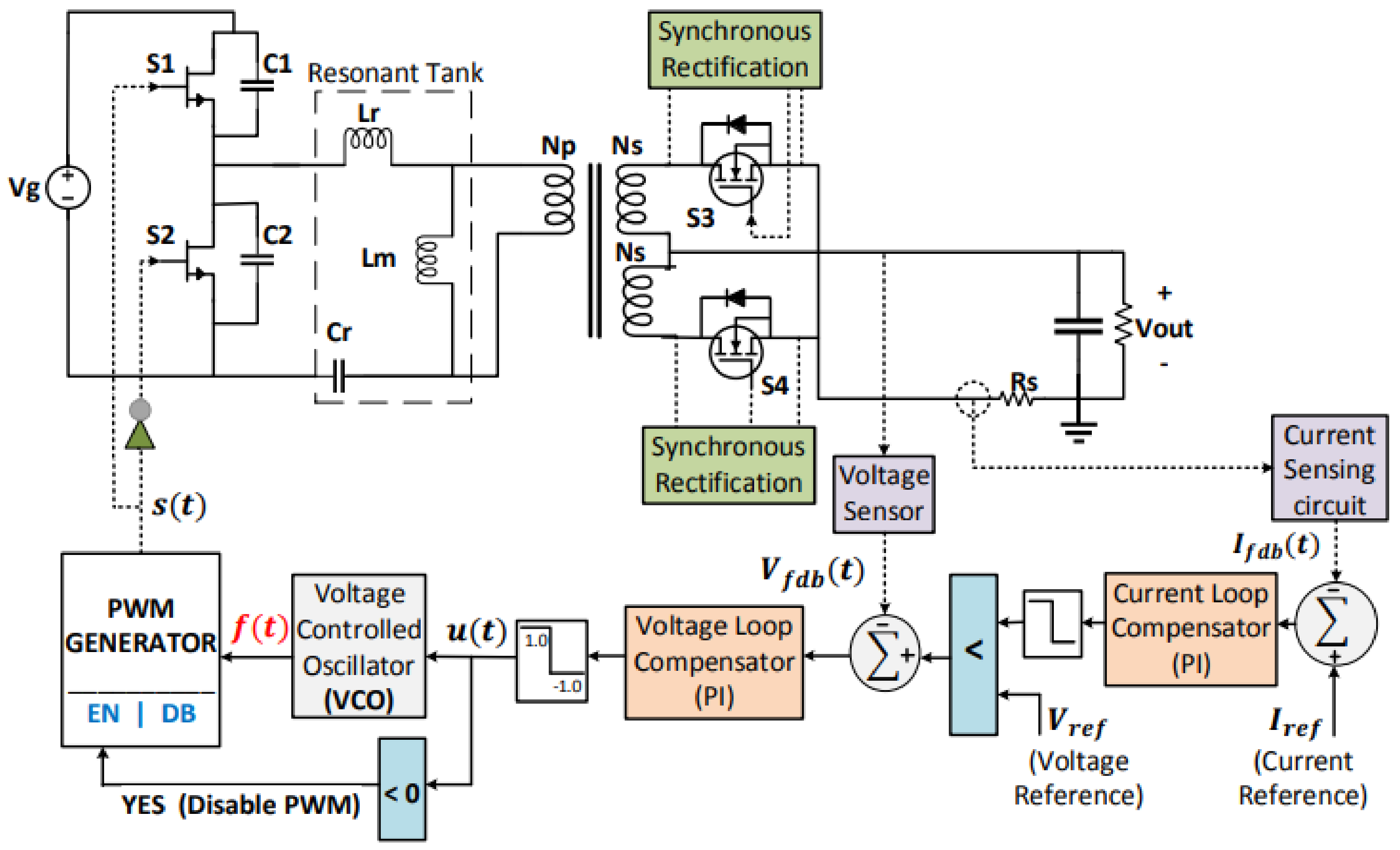
6. LLC resonant Converter Drive
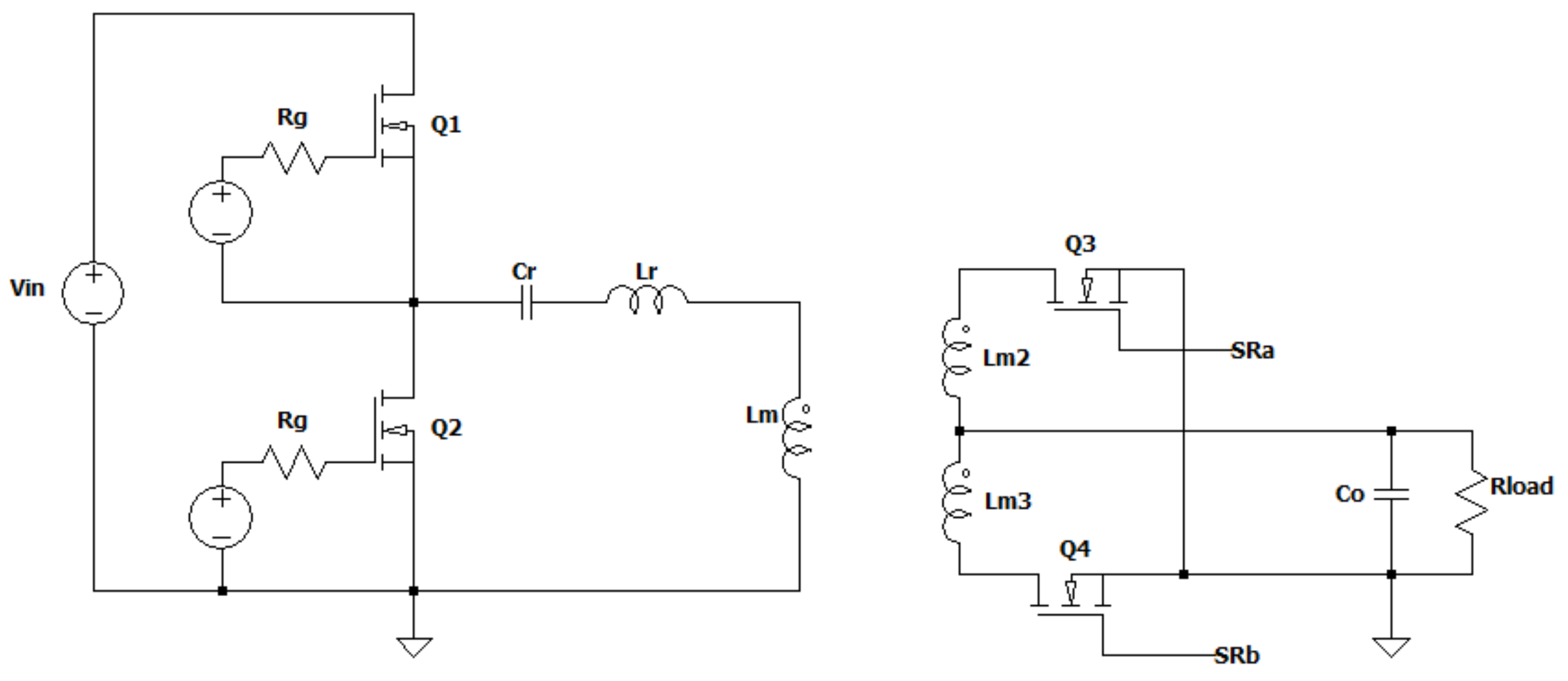
7. Interleaved LLC Resonant Converter
8. LLC inductance and Magnetics
9. Commercial Availability
10. GaN-Based LLC Converter
11. Reliability of GaN-Based Devices
12. Conclusions
Author Contributions
Funding
Institutional Review Board Statement
Informed Consent Statement
Conflicts of Interest
References
- Cornelius, A.; Hensel, A.; Wienhausen, H.A.; Kranzer, D. Application of GaN Power Transistors in a 2.5 MHz LLC DC/DC Converter for Compact and Efficient Power Conversion. In Proceedings of the 2016 18th European Conference on Power Electronics and Applications (EPE’16 ECCE Europe), Karlsruhe, Germany, 6–8 September 2016; Institute of Electrical and Electronics Engineers: Piscataway, NJ, USA, 2016; pp. 1–7. [Google Scholar]
- Amirahmadi, A.; Domb, M.; Persson, E. High Power Density High Efficiency Wide Input Voltage Range LLC Resonant Converter Utilizing E-Mode GaN Switches. In Proceedings of the 2017 IEEE Applied Power Electronics Conference and Exposition (APEC), Tampa, FL, USA, 26–30 March 2017; Institute of Electrical and Electronics Engineers: Piscataway, NJ, USA, 2017; pp. 350–354. [Google Scholar]
- Bhuvaneswari, C.; Samuel Rajesh Babu, R. A Review on LLC Resonant Converter. In Proceedings of the 2016 International Conference on Computation of Power, Energy Information and Communication (ICCPEIC), Melmaruvathur, India, 20–21 April 2016; Institute of Electrical and Electronics Engineers: Piscataway, NJ, USA, 2016; pp. 620–623. [Google Scholar]
- Huang, H. Designing an LLC Resonant Half-Bridge Power Converter. In Texas Instruments Power Supply Design Seminar, SEM1900; Topic, 3; Texas Instruments Incorporated: Dallas, TX, USA, 2010; pp. 2010–2011. [Google Scholar]
- Yang, B. Topology Investigation of Front End DC/DC Converter for Distributed Power System. Ph.D. Thesis, Department of Electrical and Computer Engineering, Virginia Tech, Blacksburg, VA, USA, 2003. [Google Scholar]
- Wen, H.; Gong, J.; Yeh, C.-H.; Han, Y.; Lai, J. An Investigation on Fully Zero-Voltage-Switching Condition for High-Frequency GaN Based LLC Converter in Solid-State-Transformer Application. In Proceedings of the 2019 IEEE Applied Power Electronics Conference and Exposition (APEC), Anaheim, CA, USA, 17–21 March 2019; Institute of Electrical and Electronics Engineers: Piscataway, NJ, USA, 2019; pp. 797–801. [Google Scholar]
- Choe, J.-M.; Yeth, C.-S.; Yu, O.; Lee, M.; Wen, H.; Lai, J.-S.; Zhang, L. Controller and EMI Filter Design for Modular Front-End Solid-State Transformer. In Proceedings of the 2018 IEEE Applied Power Electronics Conference and Exposition (APEC), San Antonio, TX, USA, 4–8 March 2018; Institute of Electrical and Electronics Engineers: Piscataway, NJ, USA, 2018; pp. 188–192. [Google Scholar]
- Deng, J.; Li, S.; Hu, S.; Mi, C.C.; Ma, R. Design Methodology of LLC Resonant Converters for Electric Vehicle Battery Chargers. IEEE Trans. Veh. Technol. 2014, 63, 1581–1592. [Google Scholar] [CrossRef]
- Chen, W.; Lu, Z.; Zhang, X.; Ye, S. A Novel ZVS Step-Up Push-Pull Type Isolated LLC Series Resonant Dc-Dc Converter for UPS Systems and Its Topology Variations. In Proceedings of the 2008 Twenty-Third Annual IEEE Applied Power Electronics Conference and Exposition, Austin, TX, USA, 24–28 February 2008; Institute of Electrical and Electronics Engineers: Piscataway, NJ, USA, 2008; pp. 1073–1078. [Google Scholar]
- Zhao, X.; Zhang, L.; Born, R.; Lai, J.S. A High-Efficiency Hybrid Resonant Converter with Wide-Input Regulation for Photovoltaic Applications. IEEE Trans. Ind. Electron. 2017, 64, 3684–3695. [Google Scholar] [CrossRef]
- Fei, C.; Gadelrab, R.; Li, Q.; Lee, F.C. High-frequency three-phase interleaved LLC resonant converter with GaN devices and integrated planar magnetics. IEEE J. Emerg. Sel. Top. Power Electron. 2019, 7, 653–663. [Google Scholar] [CrossRef]
- Hsieh, H.; Wang, H.; Huang, T. LLC charger using quasi-contactless power transfer by resonant magnetic induction coupling. IEEE Trans. Transport. Electrific. 2018, 4, 376–388. [Google Scholar] [CrossRef]
- Shen, Y.; Zhao, W.; Chen, Z.; Cai, C. Full-bridge LLC resonant converter with series-parallel connected transformers for electric vehicle on-board charger. IEEE Access 2018, 6, 13490–13500. [Google Scholar] [CrossRef]
- Shi, C.; Wang, H.; Dusmez, S.; Khaligh, A. A SiC-based high efficiency isolated on-board PEV charger with ultra-wide DC-link voltage range. IEEE Trans. Ind. Appl. 2017, 53, 501–511. [Google Scholar] [CrossRef]
- Shi, L.; Liu, B.; Duan, S. Current sharing method based on optimal phase shift control for interleaved three-phase half-bridge LLC converter with floating y-connection. J. Power Electron. 2019, 19, 934–943. [Google Scholar]
- Lee, F.C.; Wang, S.; Kong, P.; Wang, C.; Fu, D. Power Architecture Design with Improved System Efficiency, EMI and Power Density. In Proceedings of the 2008 IEEE Power Electronics Specialists Conference, Rhodes, Greece, 15–19 June 2008; Institute of Electrical and Electronics Engineers: Piscataway, NJ, USA, 2008; pp. 4131–4137. [Google Scholar]
- Chen, R.; Brohlin, P.; Dapkus, D. Design and Magnetics Optimization of LLC Resonant Converter with GaN. In Proceedings of the 2017 IEEE Applied Power Electronics Conference and Exposition (APEC), Tampa, FL, USA, 26–30 March 2017; Institute of Electrical and Electronics Engineers: Piscataway, NJ, USA, 2017; pp. 94–98. [Google Scholar]
- Yang, B.; Lee, F.C.; Zhang, A.J.; Huang, G. LLC Resonant Converter for Front end DC/DC Conversion. In Proceedings of the Seventeenth Annual IEEE Applied Power Electronics Conference and Exposition (IEEE APEC), Dallas, TX, USA, 10–14 March 2002; Institute of Electrical and Electronics Engineers: Piscataway, NJ, USA, 2002; pp. 1108–1112. [Google Scholar]
- Yang, B.; Ren, Y.; Lee, F.C. Integrated Magnetic for LLC Resonant Converter. In Proceedings of the Seventeenth Annual IEEE Applied Power Electronics Conference and Exposition (IEEE APEC), Dallas, TX, USA, 10–14 March 2002; Institute of Electrical and Electronics Engineers: Piscataway, NJ, USA, 2002; pp. 346–351. [Google Scholar]
- Lu, B.; Liu, W.; Liang, Y.; Lee, F.C.; van Wyk, J.D. Optimal Design Methodology for LLC Resonant Converter. In Proceedings of the Twenty-First Annual IEEE Applied Power Electronics Conference and Exposition (IEEE APEC), Dallas, TX, USA, 19–23 March 2006; Institute of Electrical and Electronics Engineers: Piscataway, NJ, USA, 2006; pp. 533–538. [Google Scholar]
- Fu, D.; Lu, B.; Lee, F.C. 1 MHz High Efficiency LLC Resonant Converters with Synchronous Rectifier. In Proceedings of the 2007 IEEE Power Electronics Specialists Conference (IEEE PESC), Orlando, FL, USA, 17–21 June 2007; Institute of Electrical and Electronics Engineers: Piscataway, NJ, USA, 2007; pp. 2404–2410. [Google Scholar]
- Fei, C. Optimization of LLC Resonant Converters: State-Trajectory Control and PCB based Magnetics. Ph.D. Thesis, Virginia Tech, Blacksburg, VA, USA, 2018. [Google Scholar]
- Kozacek, B.; Frivaldsky, M.; Jaros, V. Improving Qualitative Parameters of LLC Converter Using a Perspective Semiconductor and Magnetic Components. In Proceedings of the 2016 International Conference on Applied Electronics (AE), Pilsen, Czech Republic, 6–7 September 2016; Institute of Electrical and Electronics Engineers: Piscataway, NJ, USA, 2016; pp. 125–129. [Google Scholar]
- Fuhr, T.; Kupka, T. Innovative Single Stage Isolated AC/DC Converter with Power Factor Correction. In Proceedings of the 2019 20th International Scientific Conference on Electric Power Engineering (EPE), Kouty nad Desnou, Czech Republic, 15–17 May 2019; Institute of Electrical and Electronics Engineers: Piscataway, NJ, USA, 2019; pp. 1–4. [Google Scholar]
- Qiu, Y.; Lu, L.J. High-Power-Density 400VDC-19VDC LLC Solution with GaN HEMTs. In Proceedings of the 2018 1st Workshop on Wide Bandgap Power Devices and Applications in Asia (WiPDA Asia), Xi’an, China, 16–18 May 2018; Institute of Electrical and Electronics Engineers: Piscataway, NJ, USA, 2018; pp. 66–72. [Google Scholar]
- Hu, Z.; Wang, L.; Qiu, Y.; Liu, Y.-F.; Sen, P.C. An Accurate Design Algorithm for LLC Resonant Converters Part II. IEEE Trans. Power Electron. 2016, 31, 5448–5460. [Google Scholar] [CrossRef]
- Qiu, Y.; Wang, L.; Wang, H.; Liu, Y.; Sen, P.C. Bipolar Ripple Cancellation Method to Achieve Single-Stage Electrolytic-Capacitor- Less High-Power LED Driver. IEEE J. Emerg. Sel. Top. Power Electron. 2015, 3, 698–713. [Google Scholar]
- Qiu, Y.; Liu, W.; Fang, P.; Liu, Y.-F. A Mathematical Guideline for Designing an AC-DC LLC Converter with PFC. In Proceedings of the Thirty-Third Annual IEEE Applied Power Electronics Conference and Exposition (APEC 2018), San Antonio, TX, USA, 4–8 March 2018; Institute of Electrical and Electronics Engineers: Piscataway, NJ, USA, 2018; pp. 2001–2008. [Google Scholar]
- Seeman, M.D.; Bahl, S.R.; Anderson, D.I.; Shah, G.A. Advantages of GaN in a High-Voltage Resonant LLC Converter. In Proceedings of the 2014 IEEE Applied Power Electronics Conference and Exposition (APEC 2014), Fort Worth, TX, USA, 16–20 March 2014; Institute of Electrical and Electronics Engineers: Piscataway, NJ, USA, 2014; pp. 476–483. [Google Scholar]
- Reusch, D.; Lee, F.C. High Frequency Bus Converter with Low Loss Integrated Matrix Transformer. In Proceedings of the 2012 Twenty-Seventh Annual IEEE Applied Power Electronics Conference and Exposition (IEEE APEC), Orlando, FL, USA, 5–9 February 2012; Institute of Electrical and Electronics Engineers: Piscataway, NJ, USA, 2012; pp. 1392–1397. [Google Scholar]
- Huang, D.; Ji, S.; Lee, F.C. LLC Resonant Converter with Matrix Transformer. IEEE Trans. Power Electron. 2014, 29, 4339–4347. [Google Scholar] [CrossRef]
- Mu, M.; Lee, F.C. Design and Optimization of a 380–12 V High-Frequency, High-Current LLC Converter with GaN Devices and Planar Matrix Transformers. IEEE J. Emerg. Sel. Top. Power Electron. 2016, 4, 854–862. [Google Scholar]
- Mojab, A.; Hemmat, Z.; Riazmontazer, H.; Rahnamaee, A. Introducing optical cascode GaN HEMT. IEEE Trans. Electron. Devices 2017, 64, 796–804. [Google Scholar] [CrossRef]
- Fei, C.; Ahmed, M.H.; Lee, F.C.; Li, Q. Two-stage 48 V–12 V/6 V–1.8 V Voltage Regulator Module with Dynamic Bus Voltage Control for Light Load Efficiency Improvement of Two-stage Voltage Regulator. IEEE Trans. Power Electron. 2017, 32, 5628–5636. [Google Scholar] [CrossRef]
- De Groot, H.; Janssen, E.; Pagano, R.; Schetters, K. Design of a 1-MHz LLC resonant converter based on a DSP-driven SOI half-bridge power MOS module. IEEE Trans. Power Electron. 2007, 22, 2307–2320. [Google Scholar] [CrossRef]
- Fei, C.; Lee, F.C.; Li, Q. Digital Implementation of Soft Start-up and Short-circuit Protection for High-frequency LLC Converters with Optimal Trajectory Control (OTC). IEEE Trans. Power Electron. 2017, 32, 8008–8017. [Google Scholar] [CrossRef]
- Fei, C.; Lee, F.C.; Li, Q. Multi-Step Simplified Optimal Trajectory Control (SOTC) for Fast Transient Response of High Frequency LLC Converters. In Proceedings of the 2015 IEEE Energy Conversion Congress and Exposition (IEEE ECCE 2015), Montreal, QC, Canada, 20–24 September 2015; Institute of Electrical and Electronics Engineers: Piscataway, NJ, USA, 2015; pp. 2064–2071. [Google Scholar]
- Fei, C.; Li, Q.; Lee, F.C. Digital Implementation of Adaptive Synchronous Rectifier (SR) Driving Scheme for High-frequency LLC Converters with Microcontroller. IEEE Trans. Ind. Electron. 2017, 33, 5351–5361. [Google Scholar] [CrossRef]
- Fei, C.; Li, Q.; Lee, F.C. Digital implementation of light-load efficiency improvement for high-frequency LLC converters with simplified optimal trajectory control. IEEE J. Emerg. Sel. Top. Power Electron. 2018, 6, 1850–1859. [Google Scholar] [CrossRef]
- Lee, F.C.; Li, Q.; Liu, Z.; Yang, Y.; Fei, C.; Mu, M. Application of GaN devices for 1 kW server power supply with integrated magnetics. CPSS Trans. Power Electron. Appl. 2016, 1, 3–12. [Google Scholar] [CrossRef]
- Tian, M.; Hao, Y.; Wang, K.; Xuan, Y.; Huang, L.; Sun, J.; Yang, X. EMI Modeling and Experiment of a GaN Based LLC Half-Bridge Converter. In Proceedings of the 2015 9th International Conference on Power Electronics and ECCE Asia (ICPE-ECCE Asia), Seoul, Korea, 1–5 June 2015; Institute of Electrical and Electronics Engineers: Piscataway, NJ, USA, 2015; pp. 1961–1966. [Google Scholar]
- Beiranvand, R.; Rashidian, B.; Zolghadri, M.R.; Hoseini Alavi, S.M. A design procedure for optimizing the LLC resonant converter as a wide output range voltage source. IEEE Trans. Power Electron. 2012, 27, 3749–3763. [Google Scholar] [CrossRef]
- Beiranvand, R.; Rashidian, B.; Zolghadri, M.R.; Hoseini Alavi, S.M. Using LLC resonant converter for designing wide-range voltage source. IEEE Trans. Ind. Electron. 2011, 58, 1746–1756. [Google Scholar] [CrossRef]
- Wang, H.; Dusmez, S.; Khaligh, A. Design and Analysis of a Full-Bridge LLC-Based PEV Charger Optimized for Wide Battery Voltage Range. IEEE Trans. Veh. Technol. 2014, 63, 1603–1613. [Google Scholar] [CrossRef]
- Mishima, T.; Mizutani, H.; Nakaoka, M. A sensitivity-improved PFM LLC resonant full-bridge DC–DC converter with LC anti-resonant circuitry. IEEE Trans. Power Electron. 2017, 32, 310–324. [Google Scholar] [CrossRef]
- Yeon, C.; Kim, J.; Park, M.; Lee, I.; Moon, G. Improving the light load regulation capability of LLC series resonant converter using impedance analysis. IEEE Trans. Power Electron. 2017, 32, 7056–7067. [Google Scholar] [CrossRef]
- Li, C.; Wang, H.; Shang, M. A five-switch bridge based reconfigurable LLC converter for deeply depleted PEV charging applications. IEEE Trans. Power Electron. 2019, 34, 4031–4035. [Google Scholar] [CrossRef]
- Kim, C.; Baek, J.; Lee, J. High-efficiency single-stage LLC resonant converter for wide-input-voltage range. IEEE Trans. Power Electron. 2018, 33, 7832–7840. [Google Scholar] [CrossRef]
- Wu, H.; Zhan, X.; Xing, Y. Interleaved LLC resonant converter with hybrid rectifier and variable-frequency plus phase-shift control for wide output voltage range applications. IEEE Trans. Power Electron. 2017, 32, 4246–4257. [Google Scholar] [CrossRef]
- Dung, N.A.; Chiu, H.; Lin, J.; Hsieh, Y.; Chen, H.; Zeng, B. Novel modulation of isolated bidirectional DC–DC converter for energy storage systems. IEEE Trans. Power Electron. 2019, 34, 1266–1275. [Google Scholar] [CrossRef]
- Shahzad, M.I.; Iqbal, S.; Taib, S. Interleaved LLC converter with cascaded voltage-doubler rectifiers for deeply depleted PEV battery charging. IEEE Trans. Transport. Electrific. 2018, 4, 89–98. [Google Scholar] [CrossRef]
- Shang, M.; Wang, H. A voltage-quadrupler rectifier based pulse width-modulated LLC converter with wide output range. IEEE Trans. Ind. Appl. 2018, 54, 6159–6168. [Google Scholar] [CrossRef]
- Li, Z.; Xue, B.; Wang, H. An interleaved secondary-side modulated LLC resonant converter for wide output range applications. IEEE Trans. Ind. Electron. 2020, 67, 1124–1135. [Google Scholar] [CrossRef]
- Wang, H.; Li, Z. A PWM LLC type resonant converter adapted to wide output range in PEV charging applications. IEEE Trans. Power Electron. 2018, 33, 3791–3801. [Google Scholar] [CrossRef]
- Shang, M.; Wang, H.; Cao, Q. Reconfigurable LLC topology with squeezed frequency span for high-voltage bus-based photovoltaic systems. IEEE Trans. Power Electron. 2018, 33, 3688–3692. [Google Scholar] [CrossRef]
- Tang, X.; Xing, Y.; Wu, H.; Zhao, J. An improved LLC resonant converter with reconfigurable hybrid voltage multiplier and PWM-plus-PFM hybrid control for wide output range applications. IEEE Trans. Power Electron. 2020, 35, 185–197. [Google Scholar] [CrossRef]
- Sun, W.; Xing, Y.; Wu, H.; Ding, J. Modified high-efficiency LLC converters with two split resonant branches for wide input-voltage range applications. IEEE Trans. Power Electron. 2018, 33, 7867–7879. [Google Scholar] [CrossRef]
- Dao, D.N.; Lee, D.-C. High-efficiency hybrid LLC resonant converter for on-board chargers of plug-in electric vehicles. IEEE Trans. Power Electron. 2020, 35, 8324–8334. [Google Scholar]
- Matsumori, H.; Kosaka, T.; Sekido, K.; Kim, K.; Egawa, T.; Matsui, N. Isolated DC-DC Converter Utilizing GaN Power Device for Automotive Application. In Proceedings of the 2019 IEEE Applied Power Electronics Conference and Exposition (APEC), Anaheim, CA, USA, 17–21 March 2019; Institute of Electrical and Electronics Engineers: Piscataway, NJ, USA, 2019; pp. 1704–1709. [Google Scholar]
- Wen, H.; Jiao, D.; Lai, J.-S.; Strydom, J.; Zhang, L. An Accurate Voltage Gain Model Considering Diode Effect for LLC Resonant Converter in Wide Gain Range Applications. In Proceedings of the 2020 IEEE Energy Conversion Congress and Exposition (ECCE), Detroit, MI, USA, 11–15 October 2020; Institute of Electrical and Electronics Engineers: Piscataway, NJ, USA, 2020; pp. 5436–5441. [Google Scholar]
- Feng, W.; Lee, F.C.; Mattavelli, P. Optimal Trajectory Control of Burst Mode for LLC Resonant Converter. IEEE Trans. Power Electron. 2013, 28, 457–466. [Google Scholar] [CrossRef]
- Wen, H.; Jiao, D.; Lai, J.-S. Light Load Operation Analysis for MHz GaN Based LLC Resonant Converter. In Proceedings of the 2020 IEEE 9th International Power Electronics and Motion Control Conference (IPEMC2020-ECCE Asia), Seoul, Korea, 1–5 June 2015; Institute of Electrical and Electronics Engineers: Piscataway, NJ, USA, 2015; pp. 1087–1090. [Google Scholar]
- Cao, Q.; Li, Z.; Wang, H. Wide Voltage Gain Range LLC DC/DC Topologies: State-of-the-Art. In Proceedings of the 2018 International Power Electronics Conference (IPEC-Niigata 2018—ECCE Asia), Niigata, Japan, 20–24 May 2018; Institute of Electrical and Electronics Engineers: Piscataway, NJ, USA, 2018; pp. 100–107. [Google Scholar]
- Bhalsod, S.K.; Bijeev, N.V.; Jani, V.H. Design and Simulation of Advanced GaN Based LLC Resonant Converter for Space Applications. In Proceedings of the 2017 International Conference on Current Trends in Computer, Electrical, Electronics and Communication (CTCEEC), Mysore, India, 8–9 September 2017; Institute of Electrical and Electronics Engineers: Piscataway, NJ, USA, 2017; pp. 733–739. [Google Scholar]
- Glitz, E.S.; Ordonez, M. MOSFET Power Loss Estimation in LLC Resonant Converters: Time Interval Analysis. IEEE Trans. Power Electron. 2019, 34, 11964–11980. [Google Scholar] [CrossRef]
- De Simone, S.; Adragna, C.; Spini, C.; Gattavari, G. Design-oriented steady state analysis of LLC resonant converters based on FHA. In Proceedings of the SPEEDAM 2006 International Symposium on Power Electronics, Electrical Drives, Automation and Motion, Taormina, Italy, 23–26 May 2006. [Google Scholar]
- Infineon Technologies North America (IFNA) Corp. Resonant LLC Converter: Operation and Design; Application Note AN2012-09V1.0; Infineon Technologies North America (IFNA) Corp: Los Angeles, CA, USA, 2012. [Google Scholar]
- Ren, R.; Liu, B.; Jones, E.A.; Wang, F.; Zhang, Z.; Costinett, D. Accurate ZVS Boundary in High Switching Frequency LLC Converter. In Proceedings of the 2016 IEEE Energy Conversion Congress and Exposition (ECCE), Milwaukee, WI, USA, 18–22 September 2016; Institute of Electrical and Electronics Engineers: Piscataway, NJ, USA, 2016; pp. 1–6. [Google Scholar]
- Chen, H.; Wu, X. Analysis on the Influence of the Secondary Parasitic Capacitance to ZVS Transient in LLC Resonant Converter. In Proceedings of the 2014 IEEE Energy Conversion Congress and Exposition (ECCE), Pittsburgh, PA, USA, 14–18 September 2014; Institute of Electrical and Electronics Engineers: Piscataway, NJ, USA, 2014; pp. 4755–4760. [Google Scholar]
- Wen, H.; Gong, J.; Zhao, X.; Yeh, C.; Lai, J. Analysis of Diode Reverse Recovery Effect on ZVS Condition for GaN-Based LLC Resonant Converter. IEEE Trans. Power Electron. 2019, 34, 11952–11963. [Google Scholar] [CrossRef]
- Liu, J.X.; Yushyna, L. High Frequency Investigation of Wide Bandgap-based PFC and LLC Converters in PSU. In Proceedings of the PCIM Europe Digital Days 2020: International Exhibition and Conference for Power Electronics, Intelligent Motion, Renewable Energy and Energy Management, Frankfurt on the Main, Germany, 7–8 July 2020; VDE: Frankfurt on the Main, Germany; pp. 1–7. [Google Scholar]
- Strain, N.N.; Sun, J.; Huang, X.; Costinett, D.J.; Tolbert, L.M. ZVS Analysis of a GaN-Based Series-Parallel Dual Transformer LLC Resonant Converter. In Proceedings of the 2019 IEEE 7th Workshop on Wide Bandgap Power Devices and Applications (WiPDA), Raleigh, NC, USA, 29–31 October 2019; Institute of Electrical and Electronics Engineers: Piscataway, NJ, USA, 2019; pp. 398–404. [Google Scholar]
- Lee, B.; Kim, M.; Kim, C.; Park, K.; Moon, G. Analysis of LLC Resonant Converter Considering Effects of Parasitic Components. In Proceedings of the 31st International Telecommunications Energy Conference, Incheon (INTELEC 2009), Incheon, Korea, 18–22 October 2009; Institute of Electrical and Electronics Engineers: Piscataway, NJ, USA, 2009; pp. 1–6. [Google Scholar]
- Wen, H.; Liu, Y.; Lai, J.-S. Analysis on the Effect of Secondary Side Devices for the Operation of GaN Based LLC Resonant Converter. In Proceedings of the 2020 IEEE Applied Power Electronics Conference and Exposition (APEC), New Orleans, LA, USA, 15–19 March 2020; Institute of Electrical and Electronics Engineers: Piscataway, NJ, USA, 2020; pp. 2214–2218. [Google Scholar]
- Wen, H.; Jiao, D.; Lai, J.-S. Optimal Design Methodology for High Frequency GaN Based Step-up LLC Resonant Converter. In Proceedings of the 2019 IEEE 4th International Future Energy Electronics Conference (IFEEC), Singapore, 25–28 November 2019; Institute of Electrical and Electronics Engineers: Piscataway, NJ, USA, 2019; pp. 1–5. [Google Scholar]
- Wang, N.; Jia, H.; Tian, M.; Li, Z.; Xu, G.; Yang, X. Impact of Transformer Stray Capacitance on the Conduction Loss in a GaN-Based LLC Resonant Converter. In Proceedings of the 2017 IEEE 3rd International Future Energy Electronics Conference and ECCE Asia (IFEEC 2017-ECCE Asia), Kaohsiung, Taiwan, 3–7 June 2017; Institute of Electrical and Electronics Engineers: Piscataway, NJ, USA, 2017; pp. 1334–1338. [Google Scholar]
- Prieto, M.J.; Fernandez, A.; Diaz, J.M.; Lopera, J.M.; Sebastian, J. Influence of Transformer Parasitics in Low-Power Applications. In Proceedings of the Fourteenth Annual Applied Power Electronics Conference and Exposition (APEC ’99), Dallas, TX, USA, 14–18 March 1999; Institute of Electrical and Electronics Engineers: Piscataway, NJ, USA, 1999; pp. 1175–1180. [Google Scholar]
- Lu, H.-Y.; Zhu, J.-G.; Hui, S.Y.R. Experimental determination of stray capacitances in high frequency transformers. IEEE Trans. Power Electron. 2003, 18, 1105–1112. [Google Scholar]
- Saket, M.A.; Shafiei, N.; Ordonez, M.; Craeiun, M.; Botting, C. Low Parasitics Planar Transformer for LLC Resonant Battery Chargers. In Proceedings of the IEEE Applied Power Electronics Conference and Exposition, Long Beach, CA, USA, 20–24 March 2016; Institute of Electrical and Electronics Engineers: Piscataway, NJ, USA, 2016; pp. 854–858. [Google Scholar]
- Kong, P.; Wang, S.; Lee, F.C.; Wang, Z. Reducing Common-Mode Noise in Two-Switch Forward Converter. IEEE Trans. Power. Electron. 2011, 26, 1522–1533. [Google Scholar] [CrossRef]
- Zhang, W.; Long, Y.; Cui, Y.; Wang, F.; Tolbert, L.M.; Blalock, B.J.; Henning, S.; Moses, J.; Dean, R. Impact of Planar Transformer Winding Capacitance on Si-Based and GaN-Based LLC Resonant Converter. In Proceedings of the 2013 Twenty-Eighth Annual IEEE Applied Power Electronics Conference and Exposition (APEC), Long Beach, CA, USA, 17–21 March 2013; Institute of Electrical and Electronics Engineers: Piscataway, NJ, USA, 2013; pp. 1668–1674. [Google Scholar]
- Watanabe, T.; Oshikata, T.; Nishijima, K.; Kurokawa, F. A New Approach of Improvement of Dissipation Caused by Capacitance between Primary and Secondary Windings of LLC Transformer. In Proceedings of the 2015 International Conference on Renewable Energy Research and Applications (ICRERA), Palermo, Italy, 22–25 November 2015; Institute of Electrical and Electronics Engineers: Piscataway, NJ, USA, 2015; pp. 484–488. [Google Scholar]
- Saket, M.A.; Shafiei, N.; Ordonez, M. LLC converters with planar transformers: Issues and mitigation. IEEE Trans. Power Electron. 2016, 32, 4524–4542. [Google Scholar] [CrossRef]
- Chen, Y.; Lee, F.; Amoroso, L.; Wu, H.P. A Resonant MOSFET Gate Driver with Efficient Energy Recovery. IEEE Trans. Power Electron. 2004, 19, 470–477. [Google Scholar] [CrossRef]
- Eberle, W.; Zhang, Z.; Liu, Y.F.; Sen, P.C. A Current Source Gate Driver Achieving Switching Loss Savings and Gate Energy Recovery at 1-MHz. IEEE Trans. Power Electron. 2008, 23, 678–691. [Google Scholar] [CrossRef]
- Pereira, D.; de Paula, W.; Braga, H. SPICE Simulation and Evaluation of a GaN-Based Synchronous Full-Bridge Resonant Converter. In Proceedings of the 12th IEEE International Conference on Industry Applications (INDUSCON), Curitiba, Brazil, 20–23 November 2016. [Google Scholar]
- Wang, K.; Yang, X.; Wang, L.; Jain, P. Instability Analysis and Oscillation Suppression of Enhancement-Mode GaN Devices in Half-Bridge Circuits. IEEE Trans. Power Electron. 2018, 33, 1585–1596. [Google Scholar] [CrossRef]
- Yu, J.S.; Zhang, W.J.; Ng, W.T. A Segmented Output Stage H-bridge IC with Tunable Gate Driver. In Proceedings of the 2014 IEEE 26th International Symposium on Power Semiconductor Devices & IC’s (ISPSD), Waikoloa, HI, USA, 15–19 June 2014. [Google Scholar]
- Zhang, W.J.; Leng, Y.; Yu, J.S.; Jiang, X.X.; Cheng, C.Y.; Ng, W.T. A Gate Driver IC for Enhancement Mode GaN Power Transistors with Sense FET Reverse Conduction Detection Circuit. IET Power Electron. 2019, 12, 3928–3935. [Google Scholar] [CrossRef]
- Long, Y.; Zhang, W.; Costinett, D.; Blalock, B.B.; Jenkins, L.L. A High-Frequency Resonant Gate Driver for Enhancement-Mode GaN Power Devices. In Proceedings of the 2015 IEEE Applied Power Electronics Conference and Exposition (APEC), Charlotte, NC, USA, 15–19 March 2015. [Google Scholar]
- Zhang, Z.; Yang, Z.; Ye, S.; Liu, Y.-F. Topology and Analysis of a New Resonant Gate Driver. In Proceedings of the PESC Record—IEEE Annual Power Electronics Specialists Conference, Jeju, Korea, 18–22 June 2006. [Google Scholar]
- Eberle, W.; Sen, P.C.; Liu, Y.-F. A New Resonant Gate Drive Circuit with Efficient Energy Recovery and Low Conduction Loss. IEEE Trans. Ind. Electron. 2008, 55, 2213–2221. [Google Scholar] [CrossRef]
- ON Semiconductor. High Speed Half-Bridge Driver for GaN Power Switches; NCP51820; Semiconductor Components Industries, LLC.: Phoenix, AZ, USA, 2021. [Google Scholar]
- GaN Systems. Design with GaN Enhancement Mode HEMT: GN001 Application Guide; GaN Systems Inc.: Kanata, ON, Canada, 2016. [Google Scholar]
- Infineon. Single-Channel Functional and Reinforced Isolated Gate-Drive ICs for High-Voltage Enhancement-Mode GaN HEMTs; GaN EiceDRIVER Product Family; Infineon: Neubiberg, Germany, 2019. [Google Scholar]
- Yi, K.H.; Moon, G.W. Novel two-phase interleaved LLC series-resonant converter using a phase of the resonant capacitor. IEEE Trans. Ind. Electron. 2009, 56, 1815–1819. [Google Scholar]
- Hu, Z.; Qiu, Y.; Wang, L.; Liu, Y.F. An Interleaved LLC Resonant Converter Operating at Constant Switching Frequency. IEEE Trans. Power Electron. 2014, 29, 2931–2943. [Google Scholar] [CrossRef]
- Hu, Z.; Qiu, Y.; Liu, Y.F.; Sen, P.C. A control strategy and design method for interleaved LLC converters operating at variable switching frequency. IEEE Trans. Power Electron. 2014, 29, 4426–4437. [Google Scholar] [CrossRef]
- Kirshenboim, O.; Peretz, M.M. Combined Multi-Level and Two-phase Interleaved LLC Converter with Enhanced Power Processing Characteristics and Natural Current Sharing. IEEE Trans. Power Electron. 2018, 33, 5613–5620. [Google Scholar] [CrossRef]
- Orietti, E.; Mattavelli, P.; Spiazzi, G.; Adragna, C.; Gattavari, G. Current Sharing in Three-Phase LLC Interleaved Resonant Converter. In Proceedings of the 2009 IEEE Energy Conversion Congress and Exposition (IEEE ECCE 2009), San Jose, CA, USA, 20–24 September 2009; Institute of Electrical and Electronics Engineers: Piscataway, NJ, USA, 2009; pp. 1145–1152. [Google Scholar]
- Kim, H.S.; Baek, J.W.; Ryu, M.H.; Kim, J.H.; Jung, J.H. The high-efficiency isolated ac–dc converter using the three-phase interleaved LLC resonant converter employing the Y-connected rectifier. IEEE Trans. Power Electron. 2014, 29, 4017–4028. [Google Scholar] [CrossRef]
- Yang, H.; Pei, C.; Liang, Y. Magnetic Integrated Device and Power Conversion Circuit. U.S. Patent Application No. 15/147,589, 22 January 2019. [Google Scholar]
- Boysen, K.; Myhre, R. Resonant Circuit and Resonant DC/DC Converter. U.S. Patent US9240723B2, 19 January 2016. [Google Scholar]
- Nakakohara, Y.; Otake, H.; Evans, T.M.; Yoshida, T.; Tsuruya, M.; Nakahara, K. Three-phase LLC series resonant DC/DC converter using SiC MOSFETs to realize high-voltage and high-frequency operation. IEEE Trans. Ind. Electron. 2016, 63, 2103–2110. [Google Scholar] [CrossRef]
- Tengfei, O.; Noah, M.; Tsuruya, M.; Namiki, S.; Morita, K.; Imaoka, J.; Yamamoto, M. Transformer with Adjustable Path-Core Type Inductance for Use in GaN-HEMT LLC Resonant Converter. IEEJ J. Ind. Appl. 2021, 21002488. [Google Scholar] [CrossRef]
- Mostafa, N.; Kimura, S.; Imaoka, J.; Martinez, W.; Endo, S.; Yamamoto, M.; Umetani, K. Magnetic design and experimental evaluation of a commercially available single integrated transformer in three-phase LLC resonant converter. IEEE Trans. Ind. Appl. 2018, 54, 6190–6204. [Google Scholar]
- Mostafa, N.; Umetani, K.; Endo, S.; Ishibashi, H.; Imaoka, J.; Yamamoto, M. A Lagrangian dynamics model of integrated transformer incorporated in a multi-phase LLC resonant converter. In Proceedings of the 2017 IEEE Energy Conversion Congress and Exposition (ECCE), Cincinnati, OH, USA, 1–5 October 2017; Institute of Electrical and Electronics Engineers: Piscataway, NJ, USA, 2017; pp. 3781–3787. [Google Scholar]
- Mostafa, N.; Umetani, K.; Imaoka, J.; Yamamoto, M. Lagrangian dynamics model and practical implementation of an integrated transformer in multi-phase LLC resonant converter. IET Power Electron. 2018, 11, 339–347. [Google Scholar]
- Mostafa, N.; Endo, S.; Ishibashi, H.; Nanamori, K.; Imaoka, J.; Umetani, K.; Yamamoto, M. A current sharing method utilizing single balancing transformer for a multiphase LLC resonant converter with integrated magnetics. IEEE J. Emerg. Sel. Top. Power Electron. 2017, 6, 977–992. [Google Scholar]
- Krigar, T.; Pfost, M. 2-MHz Compact Wireless Power Transfer System with Voltage Conversion From 400 V to 48 V. In Proceedings of the 2021 IEEE Wireless Power Transfer Conference (WPTC), San Diego, CA, USA, 1–4 June 2021; Institute of Electrical and Electronics Engineers: Piscataway, NJ, USA, 2021; pp. 1–4. [Google Scholar]
- Ziyi, J.; Min, F.; Dou, Y.; Cao, Z.; Li, X. Optimization of key power loss for LLC circuits with planar transformer in high-frequency and high-power scenarios. AIP Adv. 2021, 11, 055119. [Google Scholar]
- Li, B.; Li, Q.; Lee, F.C. High-Frequency PCB Winding Transformer with Integrated Inductors for a Bi-Directional Resonant Converter. IEEE Trans. Power Electron. 2019, 34, 6123–6135. [Google Scholar] [CrossRef]
- Fei, C.; Lee, F.C.; Li, Q. High-Efficiency High-Power-Density LLC Converter with an Integrated Planar Matrix Transformer for High-Output Current Applications. IEEE Trans. Ind. Electron. 2017, 64, 9072–9082. [Google Scholar] [CrossRef]
- Runruo, C.; Yu, S.-Y. A High-Efficiency High-Power-Density 1MHz LLC Converter with GaN Devices and Integrated Transformer. In Proceedings of the 2018 IEEE Applied Power Electronics Conference and Exposition (APEC), San Antonio, TX, USA, 4–8 March 2018; Institute of Electrical and Electronics Engineers: Piscataway, NJ, USA, 2018; pp. 791–796. [Google Scholar]
- Yan, C.; Li, F.; Zeng, J.; Liu, T.; Ying, J. A Novel Transformer Structure for High Power, High Frequency Converter. In Proceedings of the 2007 IEEE Power Electronics Specialists Conference, Orlando, FL, USA, 17–21 June 2007; Institute of Electrical and Electronics Engineers: Piscataway, NJ, USA, 2007; pp. 214–218. [Google Scholar]
- Huang, D.; Ji, S.; Lee, F.C. LLC Resonant Converter with Matrix Transformer. In Proceedings of the 2014 IEEE Applied Power Electronics Conference and Exposition (APEC 2014), Fort Worth, TX, USA, 16–20 March 2014; Institute of Electrical and Electronics Engineers: Piscataway, NJ, USA, 2014; pp. 1118–1125. [Google Scholar]
- Ren, R.; Liu, S.; Wang, J.; Zhang, F. High Frequency LLC DC-Transformer Based on GaN Devices and the Dead Time Optimization. In Proceedings of the 2014 International Power Electronics and Application Conference and Exposition, Shanghai, China, 5–8 November 2014; Institute of Electrical and Electronics Engineers: Piscataway, NJ, USA, 2014; pp. 462–467. [Google Scholar]
- Hu, J.; Sullivan, C.R. Optimization of Shapes for Round-Wire High Frequency Gapped-Inductor Windings. In Proceedings of the 1998 IEEE Industry Applications Society Annual Meeting, St. Louis, MO, USA, 12–15 October 1998; Institute of Electrical and Electronics Engineers: Piscataway, NJ, USA, 1998; pp. 900–906. [Google Scholar]
- Pollock, J.D.; Sullivan, C.R. Modelling Foil Winding Configurations with Low AC and DC Resistance. In Proceedings of the 2005 IEEE 36th Power Electronics Specialists Conference, Recife, Dresden, Germany, 16 June 2005; Institute of Electrical and Electronics Engineers: Piscataway, NJ, USA, 2005; pp. 1507–1512. [Google Scholar]
- Wen, H.; Liu, Y.; Jiao, D.; Yeh, C.-S.; Lai, J.-S. Design Principles and Optimization Considerations of a High Frequency Transformer in GaN Based 1 MHz 2.8 kW LLC Resonant Converter with over 99% Efficiency. In Proceedings of the 2021 IEEE Applied Power Electronics Conference and Exposition (APEC), Phoenix, AZ, USA, 14–17 June 2021; Institute of Electrical and Electronics Engineers: Piscataway, NJ, USA, 2021; pp. 1939–1944. [Google Scholar]
- Liu, Y.; Wen, H.; Dung, N.A.; Lai, J. Design Considerations for MHz PCB Winding Magnetic Components. In Proceedings of the 2019 IEEE 4th International Future Energy Electronics Conference (IFEEC), Singapore, 25–28 November 2019; Institute of Electrical and Electronics Engineers: Piscataway, NJ, USA, 2019; pp. 1–8. [Google Scholar]
- Lidow, A.; Strydom, J.; Strittmatter, R.; Zhou, C. GaN: A Reliable Future in Power Conversion. IEEE Power Electron. Mag. 2015, 2, 20–26. [Google Scholar] [CrossRef]
- Ribarich, T.; Bredemeier, P.; Oliver, S. GaN High Density 300W AC-DC Converter. In Proceedings of the PCIM Europe 2019: International Exhibition and Conference for Power Electronics, Intelligent Motion, Renewable Energy and Energy Management, Nuremberg, Germany, 7–9 May 2019; VDE: Frankfurt on the Main, Germany, 2019; pp. 1–4. [Google Scholar]
- Lee, I.; Moon, G. Analysis and Design of a Three-Level LLC Series Resonant Converter for High- and Wide-Input-Voltage Applications. IEEE Trans. Power Electron. 2012, 27, 2966–2979. [Google Scholar] [CrossRef]
- Haga, H.; Kurokawa, F. Modulation Method of a Full-Bridge Three-Level LLC Resonant Converter for Battery Charger of Electrical Vehicles. IEEE Trans. Power Electron. 2017, 32, 2498–2507. [Google Scholar] [CrossRef]
- Feng, Q.; Wang, Z.; Wu, Y.; Zuk, P. 900V GaN FETs in a 300 kHz 2 kW LLC Converter for High Input Voltage Applications. In Proceedings of the 2019 IEEE 7th Workshop on Wide Bandgap Power Devices and Applications (WiPDA), Raleigh, NC, USA, 29–31 October 2019; Institute of Electrical and Electronics Engineers: Piscataway, NJ, USA, 2019; pp. 388–392. [Google Scholar]
- Ruiyang, Y.; Huang, Q.; Chen, T.; Huang, A.Q.; Ribarich, T. High-Frequency and High-Density Design of All GaN Power Supply Unit. In Proceedings of the PCIM Europe 2018: International Exhibition and Conference for Power Electronics, Intelligent Motion, Renewable Energy and Energy Management, Nuremberg, Germany, 5–7 June 2018; VDE: Frankfurt on the Main, Germany, 2018; pp. 1–5. [Google Scholar]
- Ribarich, T.; Oliver, S. State-of-The-Art GaN Power IC-Based 150 W AC-DC Adapter. In Proceedings of the PCIM Europe 2017: International Exhibition and Conference for Power Electronics, Intelligent Motion, Renewable Energy and Energy Management, Nuremberg, Germany, 16–18 May 2017; VDE: Frankfurt on the Main, Germany, 2017; pp. 1–7. [Google Scholar]
- Lee, J.Y.; Jeong, Y.S.; Han, B.M. An Isolated DC/DC Converter Using High-Frequency Unregulated LLC Resonant Converter for Fuel Cell pplications. IEEE Trans. Ind. Electron. 2011, 58, 2926–2934. [Google Scholar] [CrossRef]
- Wienhausen, A.H.; Kranzer, D. 1 MHz Resonant DC/DC-Converter Using 600 V Gallium Nitride (GaN) Power Transistors. Mater. Sci. Forum 2013, 740–742, 1123–1127. [Google Scholar] [CrossRef]
- Ruiyang, Y.; Huang, Q.; Ribarich, T.; Huang, A.Q.; Kinzer, D. Monolithic GaN Power ICs Enable High Density High Frequency 3.2 kW AC-DC Rectifier. In Proceedings of the PCIM Europe 2018: International Exhibition and Conference for Power Electronics, Intelligent Motion, Renewable Energy and Energy Management, Nuremberg, Germany, 5–7 June 2018; VDE: Frankfurt on the Main, Germany, 2018; pp. 1–4. [Google Scholar]
- Youhao, X.; Min, C.; Nielson, K.; Bell, R. Optimization of the Drive Circuit for Enhancement Mode Power GaN FETs in DC-DC Converters. In Proceedings of the Applied Power Electronics Conference and Exposition (APEC), 2012 Twenty-Seventh Annual IEEE, Orlando, FL, USA, 5–9 February 2012; Institute of Electrical and Electronics Engineers: Piscataway, NJ, USA, 2012; pp. 2467–2471. [Google Scholar]
- Sun, T.; Ren, X.; Chen, Q.; Zhang, Z.; Ruan, X. Reliability and Efficiency Improvement in LLC Resonant Converter by Adopting GaN Transistor. In Proceedings of the 2015 IEEE Applied Power Electronics Conference and Exposition (APEC ’2015), Charlotte, NC, USA, 15–19 March 2015; Institute of Electrical and Electronics Engineers: Piscataway, NJ, USA, 2015; pp. 2459–2463. [Google Scholar]
- Park, H.P.; Jung, J.H. Design Considerations of 1 MHz LLC Resonant Converter with GaN E-HEMT. In Proceedings of the 17th European Conference on Power Electronics and Applications (EPE’15 ECCE-Europe), Geneva, Switzerland, 8–10 September 2015. [Google Scholar]
- Hariya, A.; Matsuura, K.; Yanagi, H.; Tomioka, S.; Ishizuka, Y.; Ninomiya, T. 5 MHz PWM-Controlled Current Mode Resonant DC-DC Converter Using GaN-FETs. In Proceedings of the 2014 International Power Electronics Conference (IPEC-Hiroshima 2014—ECCE-ASIA), Hiroshima, Japan, 18–21 May 2014; Institute of Electrical and Electronics Engineers: Piscataway, NJ, USA, 2014; pp. 3630–3637. [Google Scholar]
- Liang, W.; Raymond, L.; Gu, L.; Rivas, J. 27.12 MHz GaN Resonant Power Converter with PCB Embedded Resonant Air Core Inductors and Capacitors. In Proceedings of the 2015 IEEE Energy Conversion Congress and Exposition (ECCE), Montreal, QC, Canada, 20–24 September 2015; Institute of Electrical and Electronics Engineers: Piscataway, NJ, USA, 2015; pp. 4251–4256. [Google Scholar]
- Shigematsu, H.; Inoue, Y.; Akasegawa, A.; Yamada, M.; Masuda, S.; Kamada, Y.; Yamada, A.; Kanamura, M.; Ohki, T.; Makiyama, K.; et al. C-Band 340W and X-Band 100W GaN Power Amplifiers with Over 50% PAE. In Proceedings of the IEEE MTT-S International Microwave Symposium Digest, Boston, MA, USA, 7–12 June 2009; Institute of Electrical and Electronics Engineers: Piscataway, NJ, USA, 2009; pp. 1265–1268. [Google Scholar]
- Micovic, M.; Kurdoghlian, A.; Shinohara, K.; Burnham, S.; Milosavljevic, I.; Hu, M.; Corrion, A.; Fung, A.; Lin, R.; Samoska, L.; et al. W-Band GaN MMIC with 842 mW Output Power at 88 GHz. In Proceedings of the IEEE MTT-S International Microwave Symposium Digest, Anaheim, CA, USA, 23–28 May 2010; Institute of Electrical and Electronics Engineers: Piscataway, NJ, USA, 2010; pp. 237–239. [Google Scholar]
- Yang, Y.; Liu, Z.; Lee, F.C.; Li, Q. Analysis and Filter Design of Differential Mode EMI Noise for GaN-Based Interleaved MHz Critical Mode PFC Converter. In Proceedings of the 2014 IEEE Energy Conversion Congress and Exposition (ECCE), Pittsburgh, PA, USA, 14–18 September 2014; Institute of Electrical and Electronics Engineers: Piscataway, NJ, USA, 2014; pp. 4784–4789. [Google Scholar]
- Mausamjeet, K.; Pervaiz, S.; Afridi, K.K. Control of a Merged-Energy-Buffer Based Two-Stage Electrolytic-Free Offline LED Driver. In Proceedings of the 2019 20th Workshop on Control and Modeling for Power Electronics (COMPEL), Toronto, ON, Canada, 17–20 June 2019; Institute of Electrical and Electronics Engineers: Piscataway, NJ, USA, 2019; pp. 1–6. [Google Scholar]
- Ionascut-Nedelcescu, A.; Carlone, C.; Houdayer, A.; von Bardeleben, J.H.; Cantin, J.L.; Raymond, S. Radiation hardness of gallium nitride. IEEE Trans. Nucl. Sci. 2002, 49, 2733–2738. [Google Scholar] [CrossRef]
- Adell, P.C.; Scheick, L.Z. Radiation Effects in Power Systems: A Review. IEEE Trans. Nucl. Sci. 2013, 60, 1929–1952. [Google Scholar] [CrossRef]
- Maier, D.; Alomari, M.; Grandjean, N.; Carlin, J.; Diforte-Poisson, M.; Dua, C.; Delage, S.; Kohn, E. InAlN/GaN HEMTs for operation in the 1000 °C regime: A first experiment. IEEE Electron. Device Lett. 2012, 33, 985–987. [Google Scholar] [CrossRef]
- Stocco, A. Reliability and Failure Mechanisms of GaN HEMT Devices Suitable for High-Frequency and High-Power Applications. Ph.D. Thesis, University of Padova, Padova, Italy, 2012. [Google Scholar]
- Meneghesso, G.; Meneghini, M.; Tazzoli, A.; Ronchi, N.; Stocco, A.; Chini, A.; Zanoni, E. Reliability issues of Gallium Nitride High Electron Mobility Transistors. Int. J. Microw. Wirel. Technol. 2006, 2, 39–50. [Google Scholar] [CrossRef]
- Shigekawa, N.; Shiojima, K.; Suemitsu, T. Electroluminescence characterization of AlGaN/GaN high-electron-mobility transistors. Appl. Phys. Lett. 2001, 79, 1196–1198. [Google Scholar] [CrossRef]
- Shigekawa, N.; Shiojima, K.; Suemitsu, T. Optical study of high-biased AlGaN/GaN high-electron-mobility transistors. J. Appl. Phys. 2002, 92, 531–535. [Google Scholar] [CrossRef]
- Meneghesso, G.; Verzellesi, G.; Danesin, F.; Rampazzo, F.; Zanon, F.; Tazzoli, A.; Meneghini, M.; Zanoni, E. Reliability of GaN High-Electron-Mobility Transistors: State of the art and perspectives. IEEE Trans. Device Mater. Reliab. 2008, 8, 332–343. [Google Scholar] [CrossRef]
- Coffie, R.; Chen, Y.; Smorchkova, I.P.; Heying, B.; Gambin, V.; Sutton, W.; Chou, Y.C.; Luo, W.-B.; Wojtowicz, M.; Oki, A. Temperature and Voltage Dependent RF Degradation Study in AlGaN/GaN HEMTs. In Proceedings of the IEEE International Reliability Physics Symposium, Phoenix, AZ, USA, 15–19 April 2007; Institute of Electrical and Electronics Engineers: Piscataway, NJ, USA, 2007; pp. 568–569. [Google Scholar]
- Vetury, R.; Zhang, N.Q.; Keller, S.; Mishra, U.K. The impact of surface states on the DC and RF characteristics of AlGaN/GaN HFETs. IEEE Trans. Electron. Devices 2001, 48, 560–566. [Google Scholar] [CrossRef]
- Chini, A.; Buttari, D.; Coffie, R.; Shen, L.; Heikman, S.; Chakraborty, A.; Keller, S.; Mishra, U.K. High Performance AlGaN/GaN HEMTs with a Field Plated Gate Structure. In Proceedings of the International Semiconductor Device Research Symposium, Washington, DC, USA, 10–12 December 2003; Institute of Electrical and Electronics Engineers: Piscataway, NJ, USA, 2003; pp. 434–435. [Google Scholar]
- Zanoni, E.; Meneghini, M.; Chini, A.; Marcon, D.; Meneghesso, G. AlGaN/GaN-based HEMTs failure physics and reliability: Mechanisms affecting gate edge and Schottky junction. IEEE Trans. Electron. Devices 2013, 60, 3119–3131. [Google Scholar] [CrossRef]
- Abbate, C.; Busatto, G.; Sanseverino, A.; Tedesco, D.; Velardi, F. Failure mechanisms of enhancement mode GaN power HEMTs operated in short circuit. Microelectron. Reliab. 2019, 100–101, 113454. [Google Scholar] [CrossRef]
- Abbate, C.; Busatto, G.; Sanseverino, A.; Tedesco, D.; Velardi, F. Failure analysis of 650 V enhancement mode GaN HEMT after short circuit tests. Microelectron. Reliab. 2018, 88–90, 677–683. [Google Scholar] [CrossRef]
- Abbate, C.; Busatto, G.; Sanseverino, A.; Tedesco, D.; Velardi, F. Experimental study of the instabilities observed in 650 V enhancement mode GaN HEMT during short circuit. Microelectron. Reliab. 2017, 76–77, 314–320. [Google Scholar] [CrossRef]
- Abbate, C.; Colella, L.; di Folco, R.; Busatto, G.; Martano, E.; Palazzo, S.; Sanseverino, A.; Velardi, F. An Accurate Switching Current Measurement Based on Resistive Shunt Applied to Short Circuit GaN HEMT Characterization. Appl. Sci. 2021, 11, 9138. [Google Scholar] [CrossRef]
- Mao, M.; Tang, S.; Wang, Z.; Deng, R.; Deng, C.; Chen, S.; Ren, Y. Effect of Temperature Cycling, High Temperature Storage and Steady-State Operation Life Test on Reliability of GaN HEMTs. In Proceedings of the 2021 22nd International Conference on Electronic Packaging Technology (ICEPT), Xiamen, China, 14–17 September 2021; Institute of Electrical and Electronics Engineers: Piscataway, NJ, USA, 2021; pp. 1–4. [Google Scholar]
- Zeng, C.; Wang, Y.; Liao, X.; Li, R.; Chen, Y.; Lai, P.; Huang, Y.; En, Y. Reliability Assessment of Algangan Hemts for High Voltage Applications Based on High Temperature Reverse Bias Test. In Proceedings of the 2014 10th International Conference on Reliability, Maintainability and Safety (ICRMS), Guangzhou, China, 6–8 August 2014; Institute of Electrical and Electronics Engineers: Piscataway, NJ, USA, 2014; pp. 298–301. [Google Scholar]


| Properties | GaN | Si | SiC |
|---|---|---|---|
| 3.4 | 1.12 | 3.2 | |
| 3.3 | 0.3 | 2.2 | |
| 210−10 | 11010 | 810−9 | |
| 2.5 | 1.0 | 2.0 | |
| 990–2000 | 1500 | 650 | |
| 1.3 | 1.5 | 3.8 |
| Technology /Parameter | GaN | Si | SiC |
|---|---|---|---|
| Part number | GS66508B-TR | FCB099N65S3 | SCT3080AW7TL |
| Manufacturer | GaN Systems | ON Semiconductor | ROHM Semiconductor |
| Drain-source voltage (V) | 650 | 650 | 650 |
| Drain current–continuous (A) | 30 | 30 | 29 |
| Rds–on () | 63 | 99 | 104 |
| Vgs (V) | −10, +7 | 4.5 | 5.6 |
| Qg–gate charge (nC) | 6.1 | 61 | 48 |
| Price $ | 15.75 | 3.67 | 12.67 |
| Parameter | Value | Parameter | Value |
|---|---|---|---|
| kHz | |||
| 0.61 | |||
| 0.68 | |||
| µH | |||
| 6.97 Ω | µH | ||
| 7.66 Ω | nF |
Publisher’s Note: MDPI stays neutral with regard to jurisdictional claims in published maps and institutional affiliations. |
© 2021 by the authors. Licensee MDPI, Basel, Switzerland. This article is an open access article distributed under the terms and conditions of the Creative Commons Attribution (CC BY) license (https://creativecommons.org/licenses/by/4.0/).
Share and Cite
Mortazavizadeh, S.A.; Palazzo, S.; Amendola, A.; De Santis, E.; Di Ruzza, D.; Panariello, G.; Sanseverino, A.; Velardi, F.; Busatto, G. High Frequency, High Efficiency, and High Power Density GaN-Based LLC Resonant Converter: State-of-the-Art and Perspectives. Appl. Sci. 2021, 11, 11350. https://0-doi-org.brum.beds.ac.uk/10.3390/app112311350
Mortazavizadeh SA, Palazzo S, Amendola A, De Santis E, Di Ruzza D, Panariello G, Sanseverino A, Velardi F, Busatto G. High Frequency, High Efficiency, and High Power Density GaN-Based LLC Resonant Converter: State-of-the-Art and Perspectives. Applied Sciences. 2021; 11(23):11350. https://0-doi-org.brum.beds.ac.uk/10.3390/app112311350
Chicago/Turabian StyleMortazavizadeh, Seyed Abolfazl, Simone Palazzo, Arturo Amendola, Enzo De Santis, Dario Di Ruzza, Giuseppe Panariello, Annunziata Sanseverino, Francesco Velardi, and Giovanni Busatto. 2021. "High Frequency, High Efficiency, and High Power Density GaN-Based LLC Resonant Converter: State-of-the-Art and Perspectives" Applied Sciences 11, no. 23: 11350. https://0-doi-org.brum.beds.ac.uk/10.3390/app112311350