Article

Design of the Class-E Power Amplifier with Finite DC Feed Inductance under Maximum-Rating Constraints

Department of Electronic Engineering, Pontificia Universidad Javeriana, Bogotá 110311, Colombia
*
Author to whom correspondence should be addressed.
Submission received: 25 February 2021 / Revised: 16 March 2021 / Accepted: 16 March 2021 / Published: 21 April 2021
(This article belongs to the Section Electrical, Electronics and Communications Engineering)

Abstract

:
This paper proposes an analytical expression set to determine the maximum values of currents and voltages in the Class-E Power Amplifier (PA) with Finite DC-Feed Inductance (FDI) under the following assumptions—ideal components (e.g., inductors and capacitors with infinite quality factor), a switch with zero rise and fall commutation times, zero on-resistance, and infinite off-resistance, and an infinite loaded quality factor of the output resonant circuit. The developed expressions are the average supply current, the RMS (Root Mean Square) current through the DC-feed inductance, the peak voltage and current in the switch, the RMS current through the switch, the peak voltages of the output resonant circuit, and the peak voltage and current in the PA load. These equations were obtained from the circuit analysis of this ideal amplifier and curve-fitting tools. Furthermore, the proposed expressions are a useful tool to estimate the maximum ratings of the amplifier components. The accuracy of the expressions was analyzed by the circuit simulation of twelve ideal amplifiers, which were designed to meet a wide spectrum of application scenarios. The resulting Mean Absolute Percentage Error (MAPE) of the maximum-rating constraints estimation was 2.64%.

1. Introduction

The Class-E Power Amplifier (PA), shown in Figure 1, has a wide range of applications due to its high efficiency. It is used in applications such as wireless power transmission systems [1], dedicated short-range communications [2], low-power RF devices [3], induction heater systems [4], and street-lighting [5]. In general, the PA designer analyzes the DC-feed inductance (i.e., L S H in Figure 1) as an RF-choke or a finite value and designs the overall circuit to guarantee Zero Voltage Switching (ZVS) and Zero Voltage Derivative Switching (ZVDS) conditions. When the value of L S H is considered in the PA model, the designer could explore the PA design with more flexibility [6,7,8], a feature that is particularly useful in applications with many constraints as the integrated PA implementations [7,9].
In general, the models of the Class-E PA with Finite DC-Feed Inductance (FDI) are more complex than the Class-E with RF-choke models because they considered the feed current behavior in the circuit analysis [9]. Furthermore, the first analytical design equations reported in [6] appeared only 43 years after the topology was born in 1964 [10]. These equations are based on an ideal model of the Class-E PA with FDI, which considers a Class-E amplifier with ideal components (e.g., inductors and capacitors with infinite quality factor), a switch with zero rise and fall commutation times, zero on-resistance, and infinite off-resistance, and an infinite loaded quality factor of the output resonant circuit [6,8,11]. Moreover, these equations allow finding the PA circuit components values for ZVS and ZDVS with an arbitrary duty-cycle and finite dc-feed inductance (e.g., continuously ranging from Class-E with small finite drain inductance to Class-E with RF choke) without an iterative procedure [8,12,13]. Therefore, these equations allow optimizing the ideal Class-E with FDI to a particular application because the designer could explore the design space under high-efficiency operation (i.e., defined by the ZVS and ZDVS operation) to find component combinations to solve the trade-offs between specifications and restrictions [14]. On one hand, a high accuracy PA design from the analytical equations of the ideal amplifier is obtained only when the assumptions of the ideal model are fulfilled by the real implementation, which generally is difficult to accomplish [15]. On the other hand, the design of this idealized amplifier is very useful on the design of the real amplifiers because allows reducing the consumed time of the iterative CAD design (commonly used in VLSI and RF applications) [8]. For instance, in [7], the authors design an integrated Class-E PA with FDI, which was designed using its idealized model and an iterative process supported by simulation tools (i.e., Cadence Virtuoso Suite).
A successful circuit implementation depends on considering the technical, economical and reliability restrictions in the design process [16,17]. In particular, to guarantee the manufacturability and reliability of the amplifier, the designer should consider aspects such as components with commercial values, tolerances, maximum ratings, and electrical stress values (i.e., voltage, current, or power) [16,17,18]. To guarantee high PA reliability, the designer involves the component degradation (produced by the exposed to voltage and current stress) in the design process by safety margins on the maximum-ratings of the components [16,19,20]. In particular, the designer of a Class-E PA with FDI must optimize the component combination to achieve the specifications and restrictions with high-efficiency [7,21,22].
The design of the Class-E PA with FDI has been explored in several works [6,7,9,13,14,23,24,25,26,27,28,29]. The involved methodologies could be classified under three paradigms: the techniques based only on iterative tuning process (assisted by simulating or prototyping of the amplifiers) [30], the methods based only on analytical equations [6,11,28], and the procedures that combines the first two approaches [12,13,29]. The main advantage of the first approach is its accuracy (when the iterative process converges) because the directly tuning of the prototype (or a good model) allows obtaining the design goals. However, this approach is very time and resource consuming. The second approach is low-cost and low-complexity because it avoids iterative cycles using analytical equations. These equations could be explicit or implicit functions of the model parameters. Furthermore, when they are implicit, their calculation could be made with minimum computer resources. The main drawback of the second approach is the math complexity involved in the analytical circuit solution. Therefore, the design procedures must be developed assisted by a mathematical software tool, especially if the analytical model cannot summarize in an explicit set of analytical equations. The mixed approach combines the advantages of the first two methods because it uses an analytical solution of a low-complexity PA model (e.g., a fixed value of D, ideal switching device, a high value of LSH) to find the start point of an iterative design process with a more accurate PA model (or prototype). Indeed, through the involved analytical equations, the PA designer could explore the PA design space to calculate the initial component values of the amplifier. Then, an iterative tuning process starts under the circuit logic embedded in the analytical model. In this process, the PA components are tuned in simulation (or in an experimental prototype). As a result, the overall iterative process converges in few steps.
The analytical expressions proposed in [9] are commonly used in low-complexity analytical design approaches because of its simplicity and high accuracy under fixed duty cycle (D) operation of 50%. The resulting solution was based on the ideal Class-E PA with FDI model and fitting tools to simplify the analytical equations proposed by [6]. Furthermore, the circuit solution are collected in a set of explicit analytical equations (usually called as the PA design set [6,7,28]) that relates all the circuit components (e.g., L S H , L 0 ) to some circuit constrains (e.g., V D D , P O U T and ω ) using ad-hoc coefficients (i.e., K L , K C , K P , K X ), which are explicit functions of the model parameter known as q [6,9]. In addition, the authors optimize the amplifier under some application scenarios and found optimum values of the q parameter for each analyzed context. The resulting methodology provides accurate and simple analytic equations (i.e., polynomial explicit equations of the q parameter). Recently in [8], the authors proposed an analytical methodology to design the ideal Class-E PA with FDI without the fixed duty cycle restriction. They reported a systematic method to explore the search space of the proposed model in [6] using a Maple™ implementation (which is available online [8]). The authors involve in their method the specifications and restrictions in some of their study cases, they use the analytical expression of the maximum voltage of the switch proposed in [14] to involve the breakdown limit of the VLSI fabrication process as a design restriction. Although they did not develop math expressions for other common amplifier restrictions or specifications (e.g, as maximum rating constraints of the passive amplifier components or 1dB compression point), if a math expression is available, it could be added to its code easily. The resulting methodology provides accurate and simple analytic equations (i.e., polynomial and trigonometric explicit equations of the q and D parameter). To summarize, the analytical methods avoid iterative solutions with lower accuracy predictions under high values of parasitic elements of the amplifier components because the maximum amplifier efficiency of a real Class-E could be outside of the ZVS condition [15]. However, when the design specifications are not achieved following these methods, the designer could be made a tuning process under hard switching operation.
This paper proposes a set of analytical expressions to determine the maximum values of the currents and voltages present in the components of the ideal Class-E PA with FDI. These mathematical expressions are developed based on the model proposed in [6] and extended in [7], and they could be integrated easily into the design methodology proposed in [8]. To the best of the authors’ knowledge, these expressions have not been reported in the literature before. Some of these mathematical expressions are simplified using curve fitting tools. The expressions accuracy were analyzed by the simulation (carry out on the Orcad Pspice Designer ® software) of twelve ideal amplifiers, which were designed to meet a wide spectrum of application scenarios. The Mean Absolute Percentage Error (MAPE) of the estimation was 2.64%, with a standard deviation of 2.58%. Additionally, the maximum estimation error was 14.89%. The rest of the article is divided as follows. Section 2 presents the ideal Class-E PA with FDI model. Section 3 presents the basic design set of the ideal Class-E PA with FDI. Section 4 develops the maximum current and voltage expressions for each component. Section 5 reports the Class-E PA validation by simulation of the expressions found in Section 4. Finally, Section 6 and Section 7 present the conclusions and the future work, respectively.

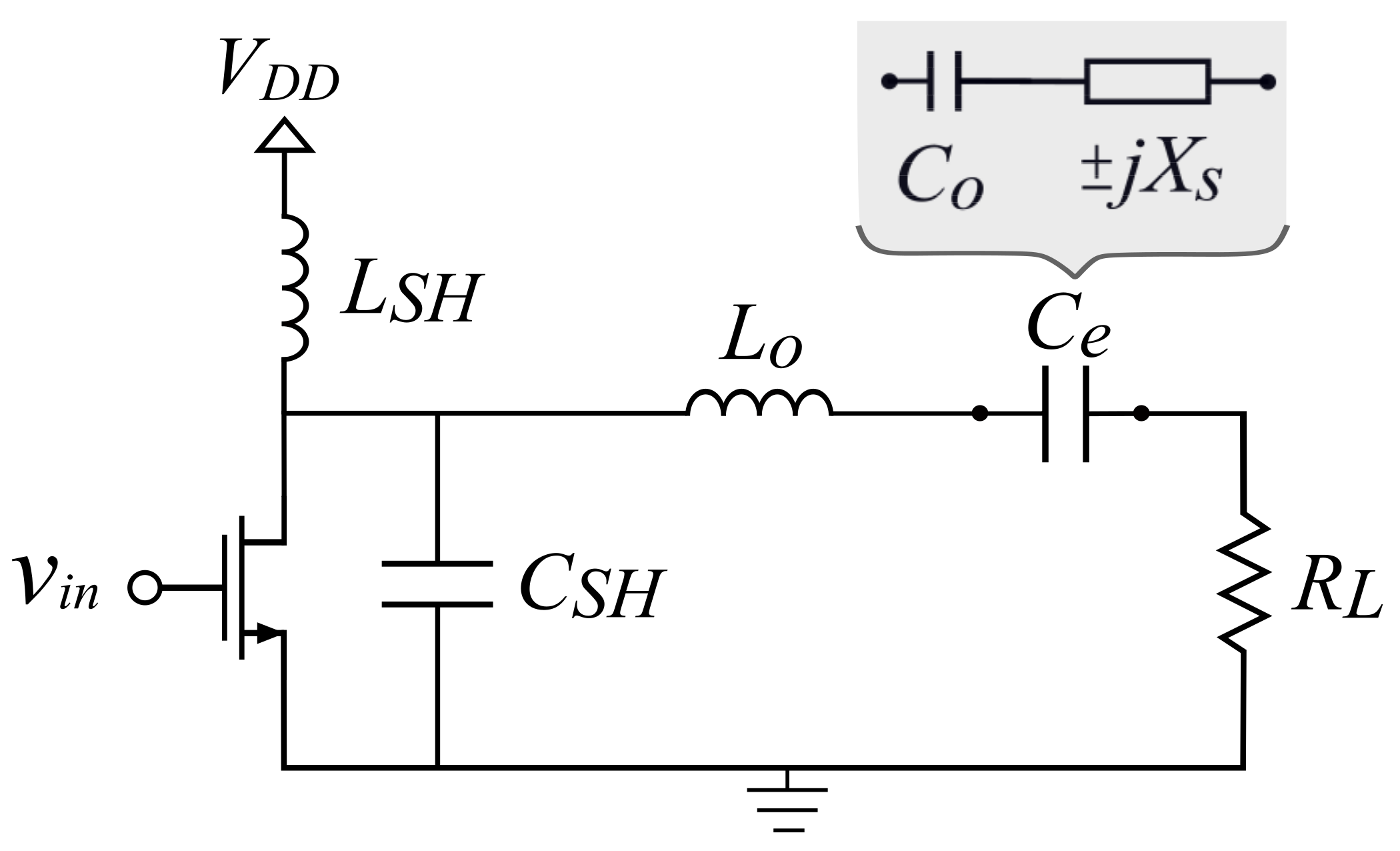
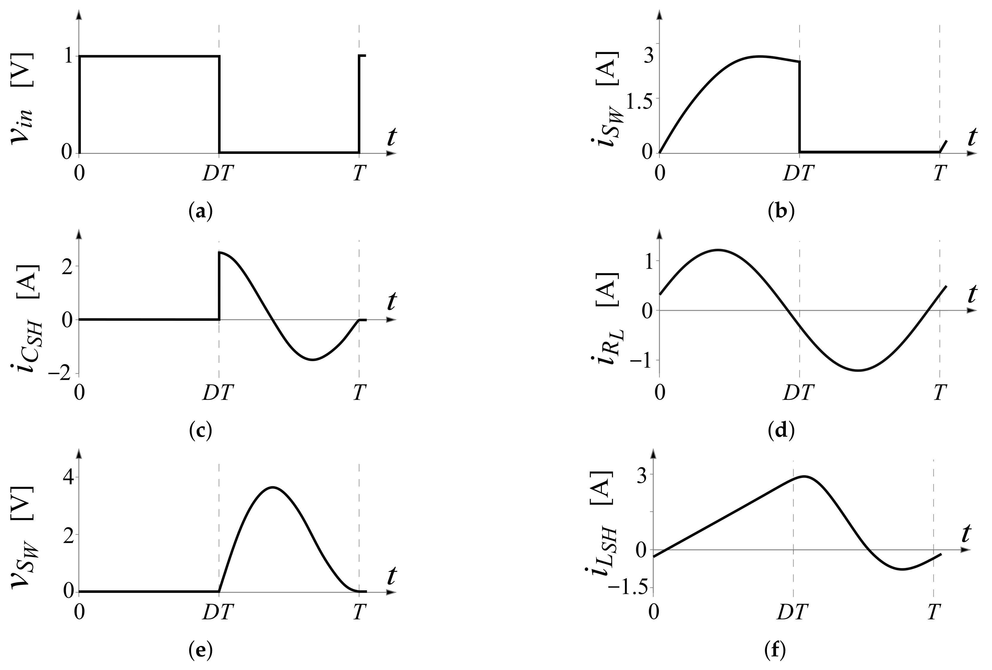
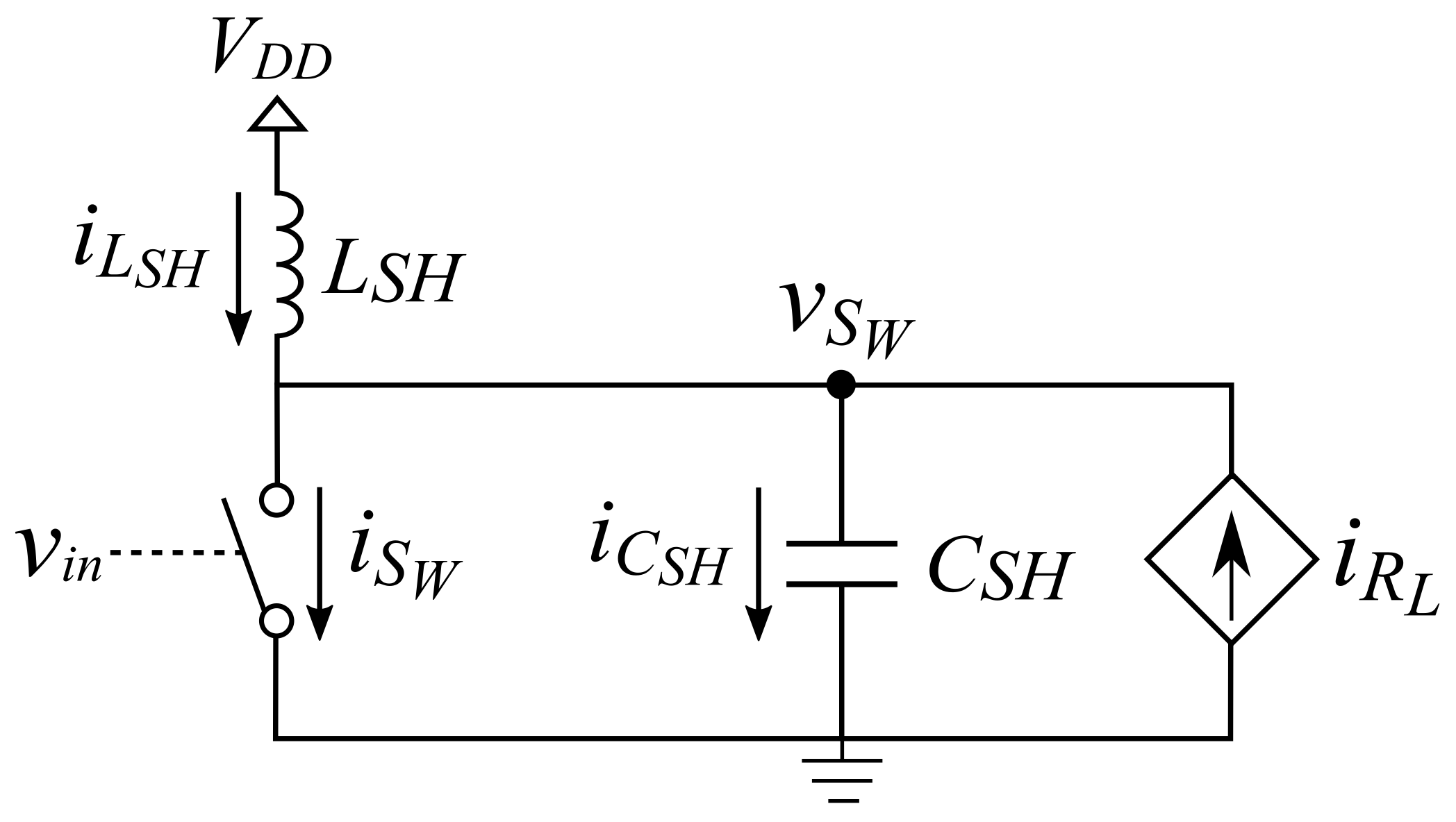
2. Ideal Class-E PA with FDI Model

The Class-E PA topology is shown in Figure 1. This amplifier is fed by a DC source ( V D D ), and by a periodical signal ( v i n ), which drives the power switch. This signal has a period T and time intervals D T and ( 1 D ) T when the switch is on and off, respectively. The main waveforms of this amplifier are shown in Figure 2. Although this topology is known for more than 50 years [10], it is still an open research topic, particularly for the Class-E PA with FDI [6]. An analytical model of this PA was proposed in [6] and extended in [7]. That model is accurate under the following assumptions: (I) it has ideal components, which means that the real power loss occurs only on R L ; (II) it has an ideal switch, with zero rise and fall commutation times, zero on-resistance, and infinite off-resistance; (III) high loaded quality factor ( Q L ) of the resonant circuit. Under the stationary response of the amplifier, the fundamental frequency of the v S w voltage is the same of the v i n , which is given by ω = 2 π / T . Therefore and according to assumption III, the voltage across the load (i.e., R L ) could be considered as a pure tone if the frequency offset (produced by the impedance X s , which is necessary to guarantee the ZVS and ZVDS operation) between ω and the natural resonance frequency of the LC output network (i.e., L o and C e ) is very low. Consequently, the load current ( i R L ) is a tone too and the PA circuit can be simplified as shown in Figure 3. It is important to notice that this high Q L model is a narrow-band approximation around the resonant frequency. The main waveforms of the ideal Class-E PA could be estimated by [6,7]
i R L ( t ) = I p s i n ( ω t + φ )
i S W ( t ) = V D D L S H t + I p s i n ( ω t + φ ) I p s i n ( φ ) 0 < t D T 0 D T < t T
v S W ( t ) = 0 0 < t D T C 1 c o s ( q ω t ) + C 2 s i n ( q ω t ) + V D D V D D q 2 1 q 2 p c o s ( ω t + φ ) D T < t T
i C S H ( t ) = 0 0 < t D T V D D L S H t 1 L S H D T t V S W ( τ ) d τ + I p ( s i n ( ω t + φ ) s i n ( φ ) ) D T < t T
i L S H ( t ) = V D D L S H t I p s i n ( φ ) 0 < t D T V D D L S H t I p s i n ( φ ) 1 L S H D T t V C S H ( τ ) d τ D T < t T ,
where I p is the peak output current, ω is the fundamental angular frequency of v i n , D is the duty cycle of v i n , which is defined as the time ratio of the switch when it is on and the total period of v i n . The variable q is defined in [6] as
q = 1 ω L S H C S H .
The model involves the variables p, φ , C 1 , and C 2 , which are functions of D and q proposed in [6]. However, the function notation was omitted in the equations for simplicity. Under this model, an infinite number of component combinations guarantee ZVS and ZVDS conditions [6,7,14]. Furthermore, to explore the best combination for a given design, the designer can tune the model parameters (i.e., the D and q). The interested reader should see [8], which detailed the ideal Class-E PA with FDI model proposed in [6] and extended in [7]. The work in [8] reported the explicit analytical expressions of the model variables (e.g., p, φ , C 1 , and C 2 ) as a function of the model parameters as well as a wide variety of study cases that show the flexibility of this analytical model.

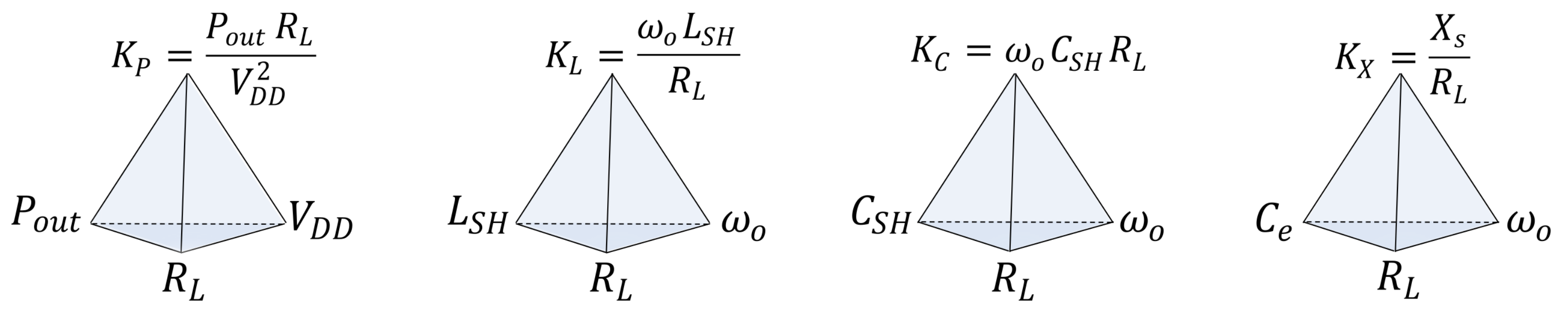
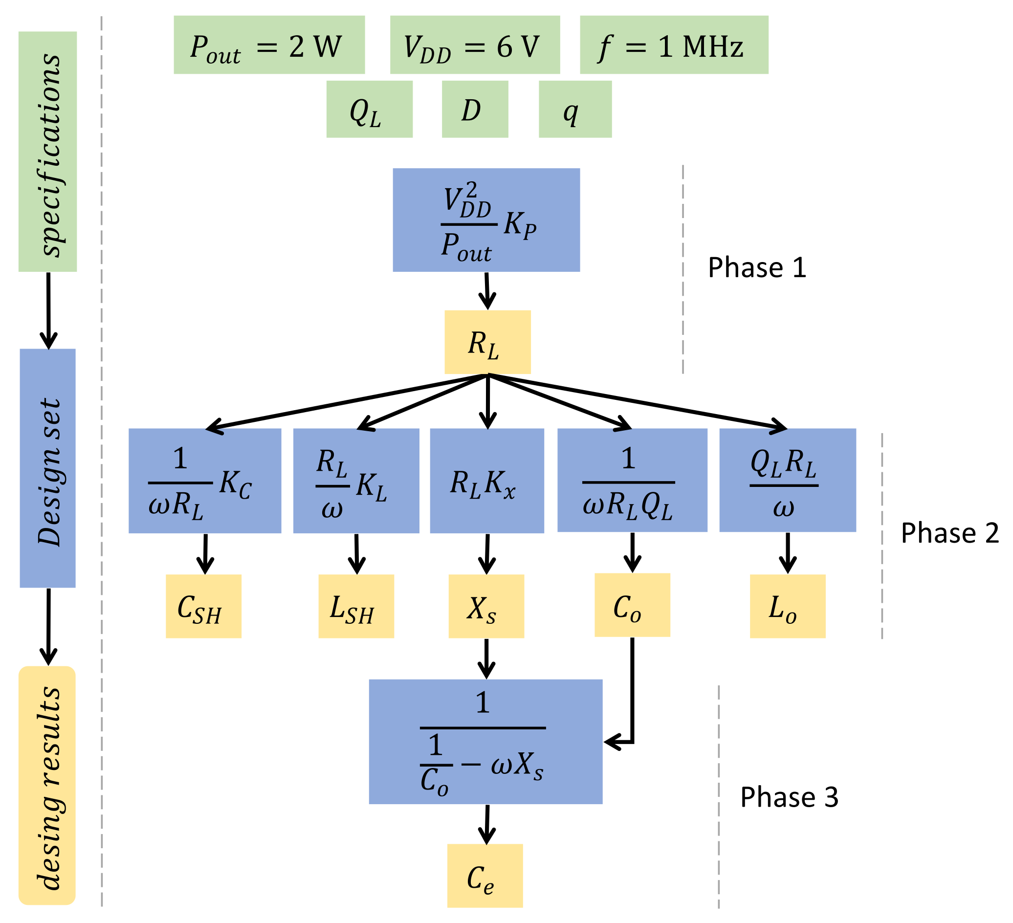
3. Basic Design set of the Ideal Class-E PA with FDI Model

Commonly, the analytical design equations are grouped in a design set K = { K L , K C , K P , K X } that relates the specifications to the PA components [6], as shown in Figure 4. For example, if the designer fixes the values of ω and R L as specifications, the K L gain can be used to find the L S H value. Therefore, to find the circuit values referred to the design specifications, the designer could use the links between the PA design variables (e.g., V D D , R L , P o u t ). According to the model summarized in Section 2, the design set are analytical functions of the variables D and q [6,7], which are
K L = ω L S H R L = p ( D , q ) 2 g x ( D , q )
K C = ω C S H R L = 2 g x ( D , q ) q 2 p ( D , q )
K P = P o u t R L V D D 2 = 2 ( g x ( D , q ) ) 2
K X = X s R L = 1 π 0 T ( v S W ( t ) c o s ( ω t + φ ) ) d t 1 π 0 T ( v S W ( t ) s i n ( ω t + φ ) ) d t ,
where X s is a capacitive or inductive reactance that must be added to the resonant network (i.e., L o and C o ) to guarantee the operation of the PA under ZVS and ZVDS conditions. Additionally and under small ripple approximation, the current gain ( g x ) is given by [14]
g x = i S W ( t ) 2 π I p ,
where m ( t ) 2 π is the moving average operator over the period of the function m ( t ) [31], which is given by
m ( t ) 2 π = 1 T 0 T m ( τ ) d τ ,
the resulting explicit g x ( D , q ) function was reported in [8].
In the design set composed of (7)–(10), the designer must fix the D and q values to design the PA from its specifications. The most popular design values are D = 0.5 and q = 1.412 because a duty cycle of 0.5 reduces the design complexity of the oscillator that controls the switch, and q = 1.412 , for a fixed V D D and R L , maximizes the load power [6].
Using this PA model, the designer can explore the design space defined by the D and q variables. The design space of q was analyzed in [9] with a practical range between 0 and 1.9 for D = 0.5 . This range allows designing the Class-E PA with lower supply voltages, low complexity impedance matching network of the load, and commercial components, among others. Moreover, the design space of D was studied in [32,33] with a practical range between 0.25 and 0.75 because D values lower than 0.25 and higher than 0.75 can produce high currents and voltages across the switch [33].

4. Proposed Analytical Expressions of the Maximum-Rating Constraints

We write this paper to motivate the use of the ideal Class-E PA with FDI and its related methodology proposed by [6,8], respectively. We propose an extension of the basic design set proposed by [8] with analytical expressions of the maximum values of currents and voltages of the PA components. The interested reader should see [8] to understand in deep the design process of this amplifier. Based on the model presented in Section 2, the analytical expressions to estimate the stress conditions supported by the components of the ideal Class-E PA with FDI are developed in this section. These equations help to involve the component restrictions (i.e., maximum rating constraints) in an early stage of the design process when the ideal model accuracy is acceptable.

4.1. Average Supply Current

The DC current of the power supply ( I 0 ) was calculated using the moving average operator [31], with the period of v i n as the time averaging window
I 0 = i L S H ( t ) 2 π = 1 T 0 T i L S H ( τ ) d τ .
Using Kirchhoff’s Current Law, (13) can be rewritten as
I 0 = i R L ( t ) 2 π + i C S H ( t ) 2 π + i S W ( t ) 2 π ,
the average currents through R L and C S H are zero. Consequently, from (2), (14) and (13), I 0 is given by [14]
I 0 = i S W ( t ) 2 π = I p g x ( D , q ) ,
where g x ( D , q ) is
g x ( D , q ) = 1 cos ( 2 π D ) 2 π cos ( φ ) + D 2 π p + sin ( 2 π D ) 2 π D sin ( φ ) .
As the PA efficiency in the model is 1 (i.e., P i n = P o u t ), the I p value can be calculated by
I p = 2 P o u t R L = 2 V D D I 0 R L
finally, I 0 is obtained by substituting (17) in (15)
I 0 = 2 V D D R L g x 2 ( D , q ) .

4.2. Peak Load Voltage

Considering PA efficiency of 1 and sinusoidal load voltage of amplitude V p , the following relation is obtained
V D D I 0 = V p 2 2 R L ,
replacing (18) in (19)
V p = 2 V D D · g x ( D , q ) .

4.3. Peak Load Current

The load current amplitude from this model could be estimated from (20), and it is given by
I p = V p R L = 2 V D D · g x ( D , q ) R L .

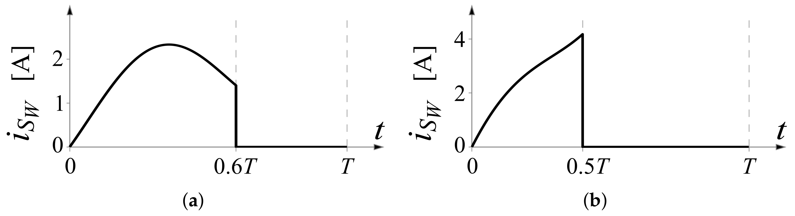
4.4. Maximum Voltage Supported by the Switch

In [14], the authors found a mathematical expression for the maximum switch voltage (and the peak voltage across the capacitor C S H ) given by
V S W M = 1.7613 + 0.0500 q 1 D V D D ,
the percentage error of this expression for a duty cycle of 0.5 is less than 2 % in the overall q range ( 0 < q < 2 ) [14]. This equation is rewritten in this article for simplicity.

4.5. Maximum Current Supported by the Switch

The switch current have a relative maximum value ( d ( i S W ( t p ) ) / d ( t p ) = 0 ) , as shown in Figure 5a. This relative maximum occurs at
t p = c o s 1 ω V D D L S H I p 1 ω φ ω = c o s 1 ω V D D R L 2 L S H V D D g x ( D , q ) 1 ω φ ω .
Moreover, the switch current presents a monotonically increasing function for some D values, as shown in Figure 5b. This behavior defines another relative maximum at the time when the switch is turning off ( t = D T ). When both relative maximums exist, the peak current of the switch is given by
I S W M = m a x i S W ( t p ) , i S W ( D T ) .
Furthermore, if (23) has not a real solution, the peak current of the switch is i S W ( D T ) .

4.6. RMS Current Supported by the Switch

The RMS current through the switch is given by
I S W R M S = 1 T 0 T i S W ( t ) 2 d t ,
substituting (2) in (25), we obtain
I S W R M S = h f I p = h f 2 V D D · g x ( D , q ) R L ,
where h f 2 is:
h f 2 = 8 π 3 D 3 3 p ( D , q ) 4 π 2 D 2 s i n ( φ ) p ( D , q ) + 2 s i n ( 2 π + φ ) p ( D , q ) 4 π D c o s ( 2 π D + φ ) p ( D , q ) s i n ( 4 π D + 2 φ ) 4 s i n ( 2 π D ) + s i n ( 2 π D + 2 φ ) π D c o s ( 2 φ ) + 2 π D 2 s i n ( φ ) p ( D , q ) 3 s i n ( 2 φ ) 4 .
The h f function was plotted in Figure 6a, in the region of interest (i.e., 0 < q < 2 , 0 < D < 1 [9]). We calculate hf varying the D and q model parameters using a 49 × 49 grid (i.e., a linearly spaced sweep from 0.01 to 0.98 and from 0.01 to 1.98 for D and q, respectively) and the math tool developed in [8], which was implemented in Maple software. These numerical data were exported to the Matlab software and were analyzed with the curve-fitting tool (i.e., cftool), in which a fitting process was performed using a non-linear least-squares method and a custom function defined by
h f ( q , D ) f 1 ( q , D ) f 2 ( q , D ) ,
where
f x ( q , D ) = a x 0 + a x 1 q + a x 2 q 2 + a x 3 D + a x 4 D 2 + a x 5 q D + a x 6 q 2 D + a x 7 q D 2 + a x 8 q 2 D 2 + a x 9 q 3 + a x 10 D 3 + a x 11 q 3 D 3 .
The coefficients of the mathematical expression found by the curve-fitting tool were summarized in Table 1. The h f fitting process has a coefficient of determination (i.e., R 2 ) of 0.9964 , and its related residuals are shown in Figure 6b. The residuals are characterized by an absolute mean error of 0.0192 and a maximum absolute error of 0.1491 , which is located at D = 0.5354 and q = 1.8979 . The graph illustrated that the fitting error is not focalized in a specific region, which indicates a low discrepancy in the overall design space between fitted values and the values expected under the ideal Class-E PA with FDI model.

4.7. Maximum Voltage Supported by C e and L o

The peak voltages of C e and L o are calculated by
V C e M = X C e ( ω ) I p
V L o M = X L o ( ω ) I p
substituting (21) in (31) and (30)
V C e M = 1 ω C e 2 V D D · g x ( D , q ) R L
V L o M = ω L o 2 V D D · g x ( D , q ) R L .

4.8. Maximum Voltage Supported by L S H

The L S H peak voltage is the difference between the peak voltage across the switch and the power supply
V L S H M = V S W M V D D ,
replacing (22) in (34)
V L S H M = 0.7613 + 0.0500 q + D 1 D V D D .

4.9. RMS Current Supported by L S H

The RMS current through the inductance L S H is given by
I L S H R M S = 1 T 0 T ( i L S H ( t ) ) 2 d t .
Solving (36), the analytical solution is
I L S H R M S = h m ( q , D ) 2 V D D · g x ( D , q ) R L ,
where h m is an extensive analytical function plotted in Figure 7a. Therefore, a curve-fitting process similar to the one discussed in Section 4.6 was used to simplify the expression. This process employed 2500 points, which corresponds to a 50 × 50 grid for the D and q variables. The D and q values were linearly swept from 0.09 to 0.92 and 0.09 to 1.92, respectively. Then, the curve-fitting of the h m data were developed using a non-linear least-squares method and the custom function defined by
h m ( q , D ) f 3 ( q , D ) f 4 ( q , D ) ,
where f 3 and f 4 use the following equation
f x ( q , D ) = b x 0 + b x 1 q + b x 2 q 2 + b x 3 D + b x 4 D 2 + b x 5 q D + b x 6 q 2 D + b x 7 q D 2 + b x 8 q 2 D 2 .
The coefficients of the mathematical expression found by the curve-fitting tool were summarized in Table 2. The h m fitting process has an R 2 of 0.9956 , and its related residuals are shown in Figure 7b. The residuals are characterized by an absolute mean error of 0.0325 and a maximum absolute error of 0.3833 , which is located at D = 0.1916 and q = 0.9863 . The graph illustrated that the fitting error is not focalized in a specific region, which indicates a low discrepancy in the overall design space between fitted values and the values expected under the ideal Class-E PA with FDI model.

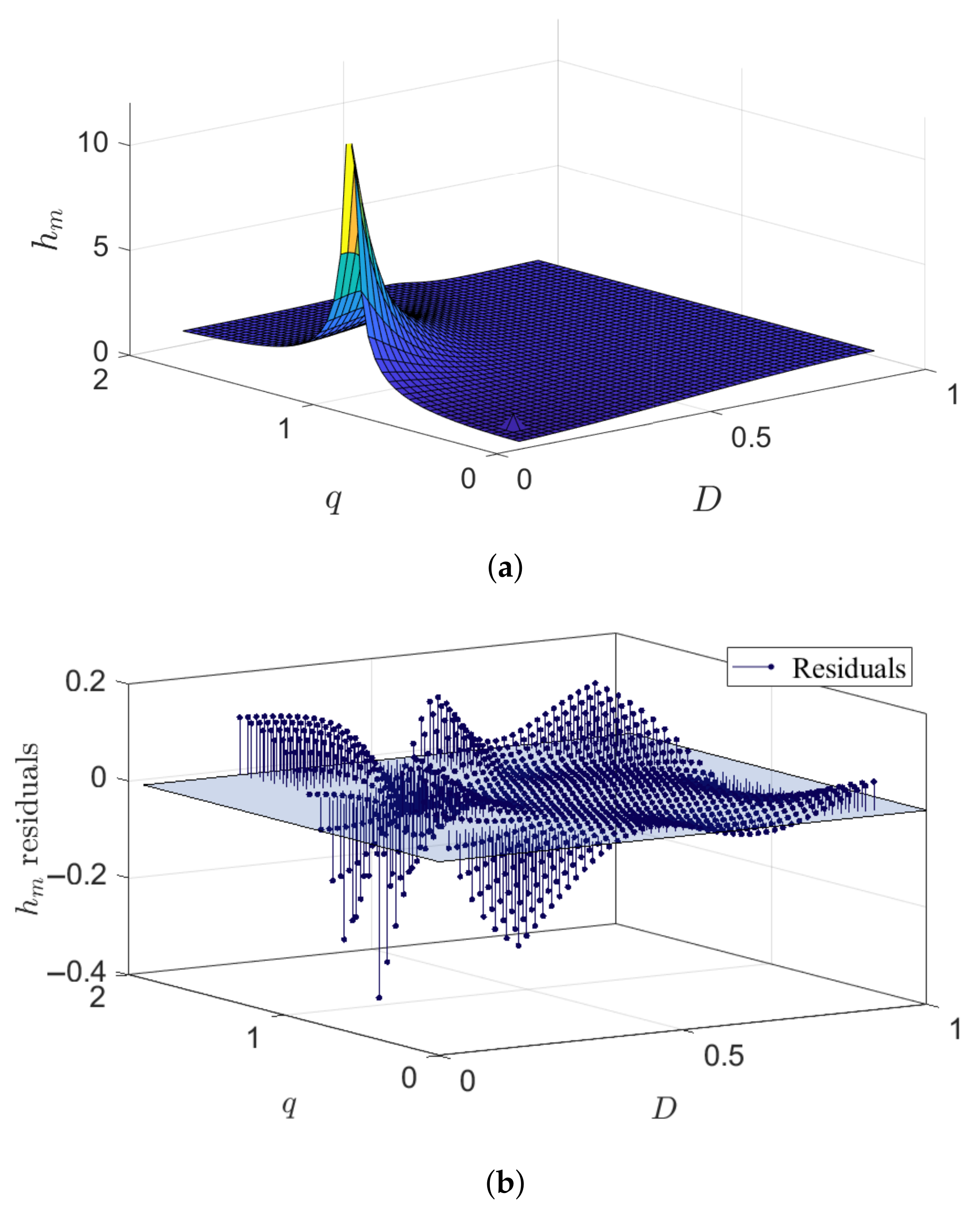
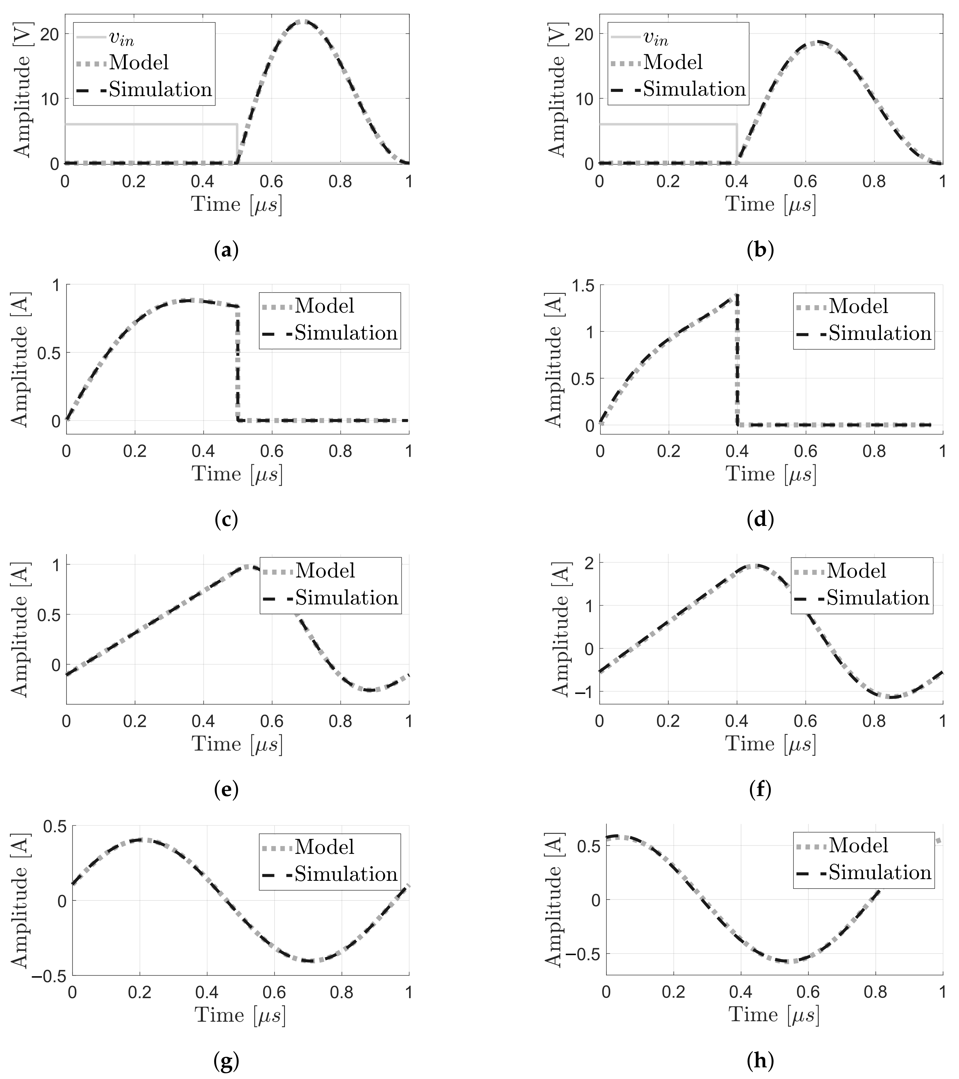
5. Accuracy of the Proposed Expressions of the Maximum-Rating Constrains

In this section, the accuracy of the expressions developed in Section 4 are evaluated. The proposed expressions were used to estimate the component maximum-rating constraints of twelve Class-E PAs with FDI. All the amplifiers were simulated in OrCAD PSpice Designer ® using transient analysis with a maximum time step of 100 ps, and simulation time of 500 s. The PA was implemented in this software using ideal components, a voltage-controlled switch with zero fall and rise times, and off-resistance and on-resistance of 1 G Ω and 1 m Ω , respectively. This setup allows the simulation of the ideal Class-E PA with FDI, which guarantees the first two assumptions of the model described in Section 2. Finally, the maximum-rating constraint estimations were compared with the simulated values and the involved error was calculated.
The specifications and model parameters of the designed amplifiers are listed in Table 3. In the first four amplifiers, the q and D variables were set to typical values (i.e., q=1.412 and D=0.5 [9]), with a parametric sweep of Q L . In the amplifiers identified by IDs four to eight, the q and Q L values were fixed to 1.412 and 20 respectively, with a parametric sweep of D. Finally, in the rest of the amplifiers the D and Q L values were fixed to 0.5 and 20 respectively, with a parametric sweep of q. The resulting model variables and the circuit components are listed in Table 4 and Table 5, respectively. These values were calculated based on the math tool proposed in [8]. Furthermore, the unknown circuit components were found following the three phases detailed in Figure 8. In this diagram the input parameters are shown in silver boxes, the relations of the design set in gray boxes, and the unknown expressions in white boxes. In phase 1, we found the equation of R L . Then, in phase 2 are identified the expressions to calculate C S H , L S H , X s , L o and C o . Finally, in phase 3 is found the C e equation.
In all designed amplifiers, the predicted and simulated waveforms present a good agreement. For instance, the waveforms of the amplifiers identified by IDs 1 and 6 are shown in Figure 9. The main stress conditions supported by the components were extracted from simulation. These results were compared to the estimated values, which were calculated from the analytical expressions proposed in Section 4. Furthermore, the MAPE was calculated as the average values of the amplifier percentage error (% Er) related to each stress parameter. The results were summarized in Table 6.
In all of the simulated amplifiers, the overall error was less than 10 % . The maximum error presented was around to 15 % in the V L o M and V C e M parameters of case four. The error can be explained by the selection of Q L value. A low Q L value produces a high estimation error because of the inaccuracy of the analytical model. Comparing all the parameters studied, V L o M and V C e M have the highest estimated error, with a MAPE of 4.15 % and 5.76 % , and a standard deviation of 3.83 % and 3.43 % , respectively. However, those errors are less significant than the error produced by the component tolerances, which typically are considered by design using a safety margin of 20 % . On the other hand, the parameter with the most accurate estimation was I S W M , which presents a MAPE of 0.59 % with a standard deviation of 0.41 % .
The estimation error related to each parameter sweep (i.e., Q L , D, and q ) is summarized in Table 7. Furthermore, this statistics (i.e., MAPE the standard deviation, and maximum and minimum values) were calculated based on the percentage errors listed in Table 6, and grouped as shown in Table 7. For instance, the statistics of the Q L sweep were calculated based on % Er of the amplifiers identified by the IDs 1, 2, 3, and 4. The highest standard deviation ( 3.48 % ) was obtained with the Q L sweep. In this sweep, the small values of Q L are critical to calculate the stress conditions reported in this paper. The highest MAPE ( 3.19 % ) was obtained with the D sweep. The highest errors are presented for extreme values of D (i.e., D = 0.3 and D = 0.7 ). Meanwhile, the parameters obtained with the sweep of q achieved a MAPE of 2.05 % , being the smallest error values of the three sweeps.
The performance of the designed amplifiers was analyzed based on its P o u t , input DC power ( P V D D ), drain efficiency ( η = P o u t / P V D D ), output second-harmonic distortion ( H D 2 ), output third-harmonic distortion ( H D 3 ), and Total Harmonic Distortion ( T H D ). These resulting Figures of Merit (FoM) were summarized in Table 8. On one hand, the P V D D and P o u t parameters had percentage errors of less than 2% concerning the theoretical value, as long as the loaded quality factor was higher or equal than 10. The simulated and theoretical η values are very similar (i.e., a perceptual error of 0.02% with a standard deviation of 0.01%). On the other hand, the H D 2 , H D 3 , and T H D had a mean value of −32.85 dBc, −48.46 dBc, and 2.75% respectively. Furthermore, the worst error prediction was presented in the study case 4, which was designed with the lowest Q L value.
The performance of the designed amplifiers was evaluated by the power and distortion FoMs, which are related to several PA applications. However, in a specific application context, other FoMs must be addressed. For instance, when the PA is embedded in a transceiver RF front-end, its non-linear FoMs (e.g, 1 dB compression point) must be analyzed.

6. Conclusions

In this paper, we propose an analytical expression set to determine the maximum values of the currents and voltages in the ideal Class-E PA with FDI components. This set was validated by simulation with a good agreement between the simulated and predicted values. The MAPE of the estimation was 2.64 % with a maximum error of 14.89 % . The proposed set can be used to estimate with low error the specifications of the circuit components (commonly referred to as the maximum ratings of the manufacturer’s datasheet) of the ideal PA. Furthermore, the approach proposed in this paper helps to involve these restrictions in an early stage of the design process when the ideal model accuracy is acceptable. This is one of the results of the first milestones reached under the framework of the research project entitled “Class-E Amplifier with Gallium Nitride Transistors for WirelessPower Transfer Applications”. The estimation accuracy is high as long as the loaded quality factor is higher than 10, the duty cycle is in the range between 0.3 and 0.7, and the q value is in the range between 0.4 and 1.6. This accuracy range covers a large number of practical applications.

7. Future Work

In the near future, we will evaluate the proposed expression accuracy using simulations with more complete component models and experimental results. Then, we will explore a more accuracy amplifier model to involve the related FoMs for a particular application in an early stage of the PA design process. For instance, if the PA is embedded in the front-end of a communication transceiver, the designer could involve the Adjacent Channel Leakage Ratio and Error Vector Magnitude. As another example, if the PA is embedded in the wireless power transfer system, the designer could involve the Power Added Efficiency. Moreover, we will explore a specific tuning process to guarantee ZVS and ZDVS operation of the amplifier when its load is an inductive link and its switch is implemented by GaN transistor.

Author Contributions

Conceptualization, all authors; methodology, all authors; software, I.C. and A.F.; validation, I.C. and A.F.; writing—original draft preparation, all authors; writing—review and editing, all authors; visualization, I.C. and A.F.; supervision, A.F., C.-I.P.-R., G.P. and M.P. All authors have read and agreed to the published version of the manuscript.

Funding

This research was funded by Pontificia Universidad Javeriana through two research projects, which were titled “Class E Amplifier with Gallium Nitride Transistors for Wireless Power Transfer Applications” and “Class-E power amplifier as an electromagnetic interference source under soft and forced switching operation”. They are identified with IDs 20066 and 09376, respectively. The APC was funded by the Pontificia Universidad Javeriana.

Institutional Review Board Statement

Not applicable.

Informed Consent Statement

Not applicable.

Data Availability Statement

The data presented in this study are available on request from the corresponding author.

Acknowledgments

This research was supported by the Pontificia Universidad Javeriana through two research projects, which were titled “Class E Amplifier with Gallium Nitride Transistors for Wireless Power Transfer Applications” and “Class-E power amplifier as an electromagnetic interference source under soft and forced switching operation”. They are identified with IDs 20066 and 09376, respectively. Additionally, the authors would like to thank the Electronics Department and Electronics laboratory of the Pontificia Universidad Javeriana, for providing the required resources to conduct this study.

Conflicts of Interest

The authors declare no conflict of interest.

Abbreviations

The following abbreviations are used in this manuscript:
PAPower Amplifier
RFRadio-Frequency
ZVSZero Voltage Switching
ZVDSZero Voltage Derivative Switching
FDIFinite DC-Feed Inductance
VLSIVery Large-Scale Integration
MAPEMean Absolute Percentage Error
RMSRoot Mean Square

References

  1. Liu, S.; Liu, M.; Han, S.; Zhu, X.; Ma, C. Tunable Class E2 DC–DC Converter with High Efficiency and Stable Output Power for 6.78-MHz Wireless Power Transfer. IEEE Trans. Power Electron. 2018, 33, 6877–6886. [Google Scholar] [CrossRef]
  2. Qaragoez, Y.M.; Ali, I.; Kim, S.J.; Lee, K. A 5.8 GHz 9.5 dBm Class-E Power Amplifier for DSRC Applications. In Proceedings of the 2019 International SoC Design Conference (ISOCC), Jeju Island, Korea, 6–9 October 2019; pp. 202–203. [Google Scholar]
  3. Silva-Pereira, M.; Caldinhas Vaz, J. A Single-Ended Modified Class-E PA with HD2 Rejection for Low-Power RF Applications. IEEE Solid-State Circuits Lett. 2018, 1, 22–25. [Google Scholar] [CrossRef]
  4. Gorain, C.; Sadhu, P.K.; Raman, R. Analysis of High-Frequency Class E Resonant Inverter and its Application in an Induction Heater. In Proceedings of the 2018 2nd International Conference on Power, Energy and Environment: Towards Smart Technology (ICEPE), Shillong, India, 1–2 June 2018; pp. 1–6. [Google Scholar]
  5. Mangkalajan, S.; Ekkaravarodome, C.; Jirasereeamornkul, K.; Thounthong, P.; Higuchi, K.; Kazimierczuk, M.K. A Single-Stage LED Driver Based on ZCDS Class-E Current-Driven Rectifier as a PFC for Street-Lighting Applications. IEEE Trans. Power Electron. 2018, 33, 8710–8727. [Google Scholar] [CrossRef]
  6. Acar, M.; Annema, A.J.; Nauta, B. Analytical Design Equations for Class-E Power Amplifiers. IEEE Trans. Circuits Syst. I Reg. Pap. 2007, 54, 2706–2717. [Google Scholar] [CrossRef] [Green Version]
  7. Fajardo, A.; de Sousa, F.R. Integrated CMOS class-E power amplifier for self-sustaining wireless power transfer system. In Proceedings of the 2016 29th Symposium on Integrated Circuits and Systems Design (SBCCI), Belo Horizonte, Brazil, 29 August–3 September 2016; pp. 1–6. [Google Scholar] [CrossRef] [Green Version]
  8. Casallas, I.; Paez-Rueda, C.I.; Perilla, G.; Pérez, M.; Fajardo, A. Design Methodology of the Class-E Power Amplifier with Finite Feed Inductance—A Tutorial Approach. Appl. Sci. 2020, 10, 8765. [Google Scholar] [CrossRef]
  9. Acar, M.; Annema, A.; Nauta, B. Generalized Design Equations for Class-E Power Amplifiers with Finite DC Feed Inductance. In Proceedings of the 36th European Microwave Conference, Manchester, UK, 10–15 September 2006; pp. 1308–1311. [Google Scholar] [CrossRef] [Green Version]
  10. Ewing, G.D. High-Efficiency Radio-Frequency Power Amplifiers. Ph.D. Thesis, Oregon State University, Corvallis, OR, USA, 1964. [Google Scholar]
  11. Kreißig, M.; Ellinger, F. Extended analysis of idealized class-E operation with finite DC-feed inductance and preservation of zero volt switching at variable load. In Proceedings of the 2017 14th International Conference on Synthesis, Modeling, Analysis and Simulation Methods and Applications to Circuit Design (SMACD), Taormina, Italy, 12–15 June 2017; pp. 1–4. [Google Scholar]
  12. Sokal, N.O. Class-E RF power amplifiers. Qex 2001, 204, 9–20. [Google Scholar]
  13. Sadeghpour, R.; Nabavi, A. Design Procedure of Quasi-Class-E Power Amplifier for Low-Breakdown-Voltage Devices. IEEE Trans. Circuits Syst. I Reg. Pap. 2014, 61, 1416–1428. [Google Scholar] [CrossRef]
  14. Fajardo, A.; de Sousa, F.R. Simple expression for estimating the switch peak voltage on the class-E amplifier with finite DC-feed inductance. In Proceedings of the 2016 IEEE 7th Latin American Symposium on Circuits & Systems (LASCAS), Florianopolis, Brazil, 28 February–2 March 2016; pp. 183–186. [Google Scholar] [CrossRef] [Green Version]
  15. Sokal, N.; Mediano, A. Redefining the optimum RF Class-E switch-voltage waveform, to correct a long-used incorrect waveform. In Proceedings of the 2013 IEEE MTT-S International Microwave Symposium Digest (MTT), Boston, MA, USA, 17–22 June 2013; pp. 1–3. [Google Scholar] [CrossRef]
  16. Özcelep, Y.; Kuntman, A.; Kuntman, H.; Yarman, S. High voltage stress effects on power MOSFETs in switching DC-DC converters. In Proceedings of the 2011 International Conference Advanced Power System Automation and Protection, Beijing, China, 16–20 October 2011; Volume 2, pp. 1278–1282. [Google Scholar]
  17. Shilo, G.; Kovalenko, D.; Gaponenko, M. Tolerance design and electronics elements’ selection under external influences. In Proceedings of the 2010 International Conference Modern Problems of Radio Engineering, Telecommunications and Computer Science (TCSET), Lviv, Ukraine, 23–27 February 2010; p. 367. [Google Scholar]
  18. Surakitbovorn, K.N.; Rivas-Davila, J.M. On the Optimization of a Class-E Power Amplifier with GaN HEMTs at Megahertz Operation. IEEE Trans. Power Electron. 2020, 35, 4009–4023. [Google Scholar] [CrossRef]
  19. Song, Y.; Lee, S.; Cho, E.; Lee, J.; Nam, S. A CMOS Class-E Power Amplifier with Voltage Stress Relief and Enhanced Efficiency. IEEE Trans. Microw. Theory Tech. 2010, 58, 310–317. [Google Scholar] [CrossRef]
  20. Jee, S.; Moon, J.; Kim, J.; Son, J.; Kim, B. Switching Behavior of Class-E Power Amplifier and Its Operation Above Maximum Frequency. IEEE Trans. Microw. Theory Tech. 2012, 60, 89–98. [Google Scholar] [CrossRef]
  21. Suetsugu, T.; Kazimierczuk, M.K. Maximum Operating Frequency of Class-E Amplifier at Any Duty Ratio. IEEE Trans. Circuits Syst. II Exp. Briefs 2008, 55, 768–770. [Google Scholar] [CrossRef]
  22. Mury, T.; Fusco, V. Exploring figures of merit associated with the suboptimum operation of class-E power amplifiers. IET Circuits Devices Syst. 2007, 1, 401–407. [Google Scholar] [CrossRef]
  23. Zulinski, R.; Steadman, J. Class E Power Amplifiers and Frequency Multipliers with finite DC-Feed Inductance. IEEE Trans. Circuits Syst. 1987, 34, 1074–1087. [Google Scholar] [CrossRef]
  24. Smith, G.H.; Zulinski, R.E. An exact analysis of class E amplifiers with finite DC-feed inductance at any output Q. IEEE Trans. Circuits Syst. 1990, 37, 530–534. [Google Scholar] [CrossRef]
  25. Li, C.; Yam, Y. Maximum frequency and optimum performance of class E power amplifiers. Proc. IEEE Circuits Devices Syst. 1994, 141, 174–184. [Google Scholar] [CrossRef]
  26. Iwadare, M.; Mori, S.; Ikeda, K. Even Harmonic Resonant Class E Tuned Power Amplifier without RF Choke. Electron. Commun. Jpn. Part 1: Commun. 1996, 79, 23–30. [Google Scholar] [CrossRef]
  27. Hasani, J.Y.; Kamarei, M. Analysis and Optimum Design of a Class E RF Power Amplifier. IEEE Trans. Circuits Syst. I Reg. Pap. 2008, 55, 1759–1768. [Google Scholar] [CrossRef]
  28. Du, X.; Nan, J.; Chen, W.; Shao, Z. ’New’ solutions of Class-E power amplifier with finite dc feed inductor at any duty ratio. IET Circuits Devices Syst. 2014, 8, 311–321. [Google Scholar] [CrossRef]
  29. Fajardo, A.; Páez, C.; Perilla, G.; Casallas, I. Design methodology of Class-E power amplifier using feed inductance tuning for high-efficiency operation in wireless power transfer applications. In Proceedings of the 2020 IEEE Conference ANDESCON, Quito, Ecuador, 13–16 October 2020. [Google Scholar]
  30. De Venuto, D.; Mezzina, G.; Rabaey, J. Automatic 3D Design for Efficiency Optimization of a Class E Power Amplifier. IEEE Trans. Circuits Syst. II Express Briefs 2018, 65, 201–205. [Google Scholar] [CrossRef]
  31. Erickson, R.W.; Maksimovic, D. Fundamentals of Power Electronics; Springer Science & Business Media: Berlin/Heidelberg, Germany, 2007; pp. 483–486. [Google Scholar]
  32. Mediano, A.; Molina-Gaudo, P.; Bernal, C. Design of Class E Amplifier with Nonlinear and Linear Shunt Capacitances for Any Duty Cycle. IEEE Trans. Microw. Theory Tech. 2007, 55, 484–492. [Google Scholar] [CrossRef]
  33. Kazimierczuk, M.; Puczko, K. Exact analysis of class E tuned power amplifier at any Q and switch duty cycle. IEEE Trans. Circuits Syst. 1987, 34, 149–159. [Google Scholar] [CrossRef]
Figure 1. Ideal model of the Class-E Power Amplifier (PA) with finite DC-feed inductance.
Applsci 11 03727 g001
Figure 2. Class-E PA ideal waveforms for duty cycle = 0.5, V D D = 1 V, and output power = 1 W. (a) v i n voltage. (b) Switch current. (c) C S H current. (d) Output current. (e) Switch voltage. (f) L S H current.
Applsci 11 03727 g002
Figure 3. High Q L model of the ideal Class-E PA with finite DC-feed inductance.
Applsci 11 03727 g003
Figure 4. Design set relations [8].
Applsci 11 03727 g004
Figure 5. Switch current behavior. (a) Waveform for D = 0.5. (b) Waveform for D = 0.4.
Applsci 11 03727 g005
Figure 6. h f graphs. (a) 3D plot. (b) Fitting residuals.
Applsci 11 03727 g006
Figure 7. h m graphs. (a) 3D plot. (b) Fitting residuals.
Applsci 11 03727 g007
Figure 8. Phases to find the unknown circuit values.
Applsci 11 03727 g008
Figure 9. Class-E PA waveforms. (a) v S W of amplifier ID 1. (b) v S W of amplifier ID 6. (c) i S W of ID 1. (d) i S W of ID 6. (e) i L S H of ID 1. (f) i L S H of ID 6. (g) i R L of ID 1. (h) i R L of ID 6.
Applsci 11 03727 g009
Table 1. Coefficients of h f .
Coefficient Name f 1 ( q , D ) f 2 ( q , D )
a x 0 0.45323.6150
a x 1 −1.2590−7.4820
a x 2 0.91593.6860
a x 3 1.2790−7.5180
a x 4 1.34407.6720
a x 5 −0.672119.4100
a x 6 0−11.8700
a x 7 0−15.7400
a x 8 −1.58909.7070
a x 9 −0.15980.1672
a x 10 0.7299−0.06993
a x 11 1.03900
Table 2. Coefficients of h m .
Coefficient Name f 3 ( q , D ) f 4 ( q , D )
b x 0 0.27690.7978
b x 1 −0.6647−1.6730
b x 2 0.46410.8805
b x 3 −0.9009−2.1030
b x 4 1.13801.8730
b x 5 2.26704.9180
b x 6 −1.6420−2.8230
b x 7 −2.3650−4.1700
b x 8 1.59202.4510
Table 3. Circuit specifications and model parameters.
ID *qD V DD
[V]
P out
[W]
f
[MHz]
Q L
11.4120.562180
21.4120.562120
31.4120.562110
41.4120.56215
51.4120.362120
61.4120.462120
71.4120.662120
81.4120.762120
90.40.562120
100.80.562120
111.20.562120
121.60.562120
* Identification number of the amplifier.
Table 4. Model variables.
ID g x ( D , q ) p ( D , q ) φ ( D , q ) C 1 ( D , q ) C 2 ( D , q )
10.831.210.2615.66−12.83
20.831.210.2615.66−12.83
30.831.210.2615.66−12.83
40.831.211.2115.66−12.83
50.250.582.17−0.36−4.54
60.580.621.333.94−8.49
70.843.83−0.4147.95−14.14
80.8714.79−0.82156.7611.79
90.5534.47−0.54−52.31−24.79
100.617.09−0.4457.87−46.62
110.752.14−0.14−9.96−46.75
120.700.930.8212.343.79
Table 5. Circuit components.
ID R L
[ Ω ]
L SH
[ μ H]
C SH
[nF]
L o
[ μ H]
C e
[pF]
124.542.864.44312.4381.07
224.542.864.4478.11324.30
324.542.864.4439.05648.58
424.542.864.4419.531297.15
52.260.4130.737.203115.95
612.061.0312.3038.38632.94
725.279.201.3880.45320.20
827.2236.840.3486.64298.12
911.0354.652.9035.10763.48
1013.5412.453.1843.10615.12
1120.454.613.8165.09397.95
1217.451.855.3555.54441.90
Table 6. Comparison of the estimated and simulated maximum-rating constrains.
Parameter \ID123456789101112MAPEStd. Dev.
Sim. a 0.330.340.340.350.340.340.340.340.340.340.340.34
I 0 [A]Cal. b 0.330.330.330.330.330.330.330.330.330.330.330.33
% Er. c 0.011.001.873.981.841.741.692.631.661.551.141.451.720.95
Sim.0.400.410.410.421.310.570.410.400.620.560.450.47
I p [A]Cal.0.400.400.400.401.330.580.400.380.600.540.440.48
% Er.0.080.901.944.841.690.923.024.843.213.062.281.482.351.50
Sim.9.9210.0010.1010.412.966.8810.3710.976.867.599.268.23
V p [V]Cal.9.919.919.919.913.016.9410.0510.436.647.369.048.35
% Er.0.080.911.954.851.760.893.004.853.253.072.291.462.361.51
Sim.21.9022.1222.3322.8016.3818.7627.7137.9721.8721.9122.0122.38
V S W M [V]Cal.21.9821.9821.9821.9815.7018.3227.4836.6421.3821.6221.8622.10
% Er.0.380.611.543.574.122.340.823.512.271.340.691.271.871.28
Sim.0.880.880.880.882.221.410.780.740.950.930.910.93
I S W M [A]Cal.0.880.880.880.882.201.390.780.730.950.940.910.92
% Er.0.330.140.490.730.601.250.301.100.440.260.161.280.590.41
Sim.0.510.510.530.540.730.620.500.490.520.520.520.54
I S W R M S [A]Cal.0.510.510.510.510.680.590.480.440.520.510.520.50
% Er.0.200.393.666.717.004.183.4010.201.010.720.056.833.703.37
Sim.784.80191.4492.4843.3263.22139.95191.33198.65137.71150.26176.63167.18
V L o M [V]Cal.792.58198.1499.0749.5460.15138.89201.09208.68132.82147.19180.88167.08
% Er.0.993.517.1314.364.850.765.105.053.552.052.400.064.153.83
Sim.800.30206.83107.6958.2174.12152.49206.84214.78132.21147.65184.75180.77
V C e M [V]Cal.792.58198.1599.0749.5467.93144.84197.74204.66125.56140.63176.89172.45
% Er.0.964.208.0014.898.355.014.404.715.034.754.264.605.763.43
Sim.15.9016.1216.3316.8010.3812.7621.7131.9715.8715.9116.0116.38
V L S H M [V]Cal.15.9815.9815.9815.989.7012.3221.4830.6415.3815.6215.8616.10
% Er.0.530.842.104.846.503.441.054.173.131.850.951.732.591.85
Sim.0.520.530.530.542.331.080.370.340.340.350.420.72
I L S H R M S [A]Cal.0.530.530.530.532.361.100.360.340.330.350.420.72
% Er.0.340.421.062.571.001.601.142.672.771.370.360.781.340.89
a Simulated value. b Calculated value. c %Er. = | S i m . C a l . | S i m . 100. The absolute percentage error was calculated using all the precision provided by each software.
Table 7. Estimation error results.
SweepAmplifier IDsMax.% Er.Min. % Er.MAPEStd. Dev.
Q L 1, 2, 3, and 414.890.012.703.48
D5, 6, 7, and 810.200.303.192.26
q9, 10, 11, and 126.830.052.051.53
Table 8. Power and distortion Figures of Merit (FoM) of the designed amplifiers.
FoMs \ID123456789101112
P V D D
[W]
Sim. a 2.002.022.042.082.042.042.032.052.032.032.022.03
Th. b 2.002.002.002.002.002.002.002.002.002.002.002.00
P o u t
[W]
Sim.2.002.022.042.082.042.042.032.052.032.032.022.03
Th.2.002.002.002.002.002.002.002.002.002.002.002.00
η [%]Sim.99.9999.9999.9999.9999.9799.9899.9899.9599.9999.9999.9999.99
Th.100.00100.00100.00100.00100.00100.00100.00100.00100.00100.00100.00100.00
H D 2
[dBc]
Sim.−47.12−34.88−28.78−22.57−31.41−34.93−32.35−30.58−31.70−32.54−34.21−33.20
Th.
H D 3
[dBc]
Sim.−63.42−51.12−44.76−38.03−49.95−56.12−43.50−38.43−47.84−48.72−50.44−49.25
Th.
T H D
[%]
Sim.0.451.833.697.562.711.802.513.242.642.391.972.22
Th.0.000.000.000.000.000.000.000.000.000.000.000.00
a Simulated value. b Theoretical value.
Publisher’s Note: MDPI stays neutral with regard to jurisdictional claims in published maps and institutional affiliations.

