
Enhanced Quasi Type-1 PLL-Based Multi-Functional Control of Single-Phase Dynamic Voltage Restorer


1
Nuclear Futures Institute, Bangor University, Bangor LL57 2DG, UK
2
Department of Electrical and Electronic Engineering, European University of Lefke, Lefke 99728, Turkey
3
Department of Computer Engineering, Eastern Mediterranean University, Mersin 10, Famagusta 99628, Turkey
4
Institut de Recherche Dupuy de Lôme (UMR CNRS 6027 IRDL), University of Brest, 29238 Brest, France
5
Logistics Engineering College, Shanghai Maritime University, Shanghai 201306, China
*
Author to whom correspondence should be addressed.
Appl. Sci. 2022, 12(1), 146; https://0-doi-org.brum.beds.ac.uk/10.3390/app12010146
Submission received: 5 November 2021
/
Revised: 20 December 2021
/
Accepted: 21 December 2021
/
Published: 24 December 2021
(This article belongs to the Special Issue Microgrids/Nanogrids Implementation, Planning, and Operation)
Abstract
:This paper considers the reference signal generation problem for the multi-functional operation of single-phase dynamic voltage restorers. For this purpose, a single-phase quasi type-1 phase-locked loop (QT1-PLL) is proposed. The pre-loop filter part of this PLL is composed of a frequency-fixed delayed signal cancellation method and a two-stage all-pass filter. Thanks to the frequency-fixed nature, the pre-loop filter is easy to implement and can provide rejection of any measurement offset. Moreover, this PLL benefits from the excellent harmonic robustness property of the conventional QT1-PLL. Small-signal modeling and gain tuning procedures are detailed in this paper. In order to track the reference voltage signals generated by the proposed PLL, a super-twisting sliding mode controller is also presented, which helps to achieve fast dynamic responses. Laboratory-scale prototype-based experimental studies were conducted to validate the developed reference generator and the controller. Experimental results show that the proposed method is fast in detecting and compensating any grid voltage anomalies to maintain constant load voltage despite voltage sag, swell, and harmonic distortions.
1. Introduction
Power quality problems such as voltage sag, swell, and harmonics can significantly affect the performance of critical loads that are used in hospital, water treatment plant, data center, etc. In addition to harmonics, voltage sag and swells are quite common in power grid and can be caused by many reasons such as lightning strike, accident, short circuit, over loading, switching on or off large electrical loads, etc. In the case of water treatment plant, voltage sag/swell can interrupt the treatment process including dissolved air flotation, filtration, and disinfection. Any interruption in the process can take up to 8 h to resolve, causing one-third production loss for the day. This highlights the importance of mitigating voltage-related power quality problems.
In order to address power quality issues such as voltage sag, swell, and harmonics, the dynamic voltage restorer (DVR) became very popular in recent times [1,2,3,4]. DVR can compensate voltage sag, swell, and harmonics to maintain desired constant voltage at the critical load side. In the literature, various topologies of DVR are proposed. However, the most basic DVR topology is made of any dc voltage source such as battery, photovoltaic panel, etc., together with a voltage source inverter with LC filter and a transformer. The transformer provides galvanic isolation between the inverter and its secondary is connected between the grid voltage and the load in series. The control system of DVR constantly monitors grid voltage and injects compensation voltage when it detects any deviation from the desired voltage. This results in maintaining desired load voltage despite various power quality disturbances at the grid.
The detection of voltage sag, swell, and harmonics plays a vital role in ensuring the effective operation of DVR. Voltage sag and swells are typically short-lived incidents with a time range of few milliseconds to a minute [5]. As such, fast and accurate detection of sag and swell is essential for fast responsive DVR operation. In the ideal case, voltage sag/swell can be detected very quickly by comparing the voltage magnitude with respect to the ideal magnitude. However, calculating the magnitude can be tricky in the presence of nonlinearities such as harmonics.
The first step in compensation voltage calculation is to generate the reference voltage, which should be in-phase with the measured grid voltage. If the grid voltage is ideal, i.e., has a frequency of (or ) and contains no harmonics, then generating the reference voltage is straightforward. However, this is not the case in practice. According to the European standard EN 50160 [6], grid voltage can vary between and of the nominal frequency. However, the grid frequency has to be within of the nominal value, i.e., Hz for of the time. Moreover, harmonics are almost always present in the grid due to the ever increasing penetration of nonlinear loads and converter-interfaced distributed energy sources. All these factors complicate the reference voltage calculation.
In order to address the non-ideal characteristics of the measured grid voltage, researchers often rely on phase-locked loop (PLL) [7,8,9,10,11,12,13,14,15] or similar techniques to generate the reference voltage for DVR. Using PLL, first, the instantaneous phase of the grid voltage fundamental component is estimated. This can then be used as the unit template for the reference voltage. By multiplying the unit template with the desired amplitude, the actual reference grid voltage can be calculated. In this study, we are considering a single-phase DVR. However, traditional PLLs in the form of synchronous reference frame (SRF) PLLs work only for three-phase systems. For single-phase systems, an additional orthogonal signal generator (OSG) is required to implement SRF-PLL. In the single-phase DVR literature, various OSGs have already been used. In [16], a second-order generalized integrator (SOGI) is used as the OSG. The effect of DC offset is not considered in [16]. Moreover, despite having band-pass filtering property, traditional SOGI-PLL cannot completely reject the dominant harmonics. Thus, multiple SOGIs need to be placed in parallel in order to reduce the effect of dominant harmonic components. This can make the overall system computationally complex. It is to be noted here that the conventional SRF-PLL can be made robust to harmonics and DC offset by considering a slow loop-filter, i.e., by reducing the bandwidth. This has been considered in [17]. Although this is an interesting practical solution, this strategy is suitable for voltage compensation but not harmonics.
Self-tuning filter (STF) is similar to SOGI; however, in the case of STF, the error feedback is independent of the grid frequency. In [18,19], the authors have applied STF as the reference generator without considering frequency adaptation. As such, the reference generator in [18,19] can be limiting when the grid frequency varies significantly. Quarter-delay is another popular method for generating orthogonal signal. This approach is considered in [20]. However, in off-nominal frequency condition, the required delay would be fractional which increases computational complexity. In [21], an adaptive notch filter (ANF) is used as the reference generator. However, the considered ANF did not use gain normalization. This can make the convergence time slow in the presence of voltage sag.
Based on the literature review, it is clear that there is demand for a reference generator that is robust to harmonics and DC offset while at the same time is computationally simple to implement. For this purpose, in this study, a quasi type-1 PLL [22,23,24] is considered. This PLL has been selected for several reasons. Firstly, it can provide amplitude normalization without using any low-pass filter unlike conventional SRF-PLL, cf. [25]. Use of additional low-pass filter in the amplitude normalization block will introduce tuning complexity as there is one more gain to tune. Secondly, this PLL provides good harmonic robustness thanks to the use of a moving-average filter. Finally, it has only one gain to tune unlike SRF-PLL where the loop-filter has two tuning parameters. However, this PLL can work only for three-phase system. Thus, a single-phase version of this PLL is proposed in this study. For this purpose, first, a half-cycle delayed signal cancellation method is applied to reject the DC offset. Then, a frequency-fixed all-pass filter (APF) [26] is applied to generate the orthogonal signal. However, single-stage APFs will generate double frequency oscillations in off-nominal frequency conditions. As such, a two-stage APF is considered that can eliminate the double frequency error. The APF is selected in this study as it can generate orthogonal signals without using any tuning gain unlike other choices available in the literature such as SOGI [16,27], ANF [21], etc. This is beneficial from the tuning simplicity point of view. Finally, the filtered grid voltage signal and its orthogonal component are used as the inputs to the quasi type-1 PLL. A small-signal model of the proposed PLL is developed and validated. Finally, tuning of the PLL gain is also presented. Compared to conventional PLL techniques summarized in [28], our approach is very simple to tune as it has only one tuning gain. All the techniques summarized in [28] have at least three parameters to tune if amplitude normalization is considered. Unlike most of the techniques in [28], our quadrature signal generator is frequency non-adaptive. As such, there is no frequency feedback which may be beneficial from the stability point of view.
Once the reference signal is generated, the role of control system is to follow/track the reference. In the literature, synchronous frame approach in the form of proportional-integral (PI) controllers [29] are widely used. Although this controller can be easily designed and implemented, the dynamic response can be slow. In order to enhance dynamic performance, advanced controllers such as model predictive control (MPC) [7,8], [30], and sliding mode control (SMC) [31,32,33] are proposed in the literature. MPC can be sensitive to model parameters mismatch. Computational complexity can be an issue for controllers. SMC is often a suitable choice for controlling nonlinear systems in the presence of parameter mismatch and/or external perturbations. As such, this technique has been selected in this study.
The rest of this article is organized as follows: Section 2 explains the operation of the proposed DVR together with the error model for controller development. Development of the proposed reference signal generator is provided in detail in Section 3. Development of the sliding-mode controller is provided in Section 4. Experimental results on a laboratory-scale prototype together with simulation results are provided in Section 5. Finally, Section 6 concludes this paper.
2. DVR Modeling and Problem Formulation
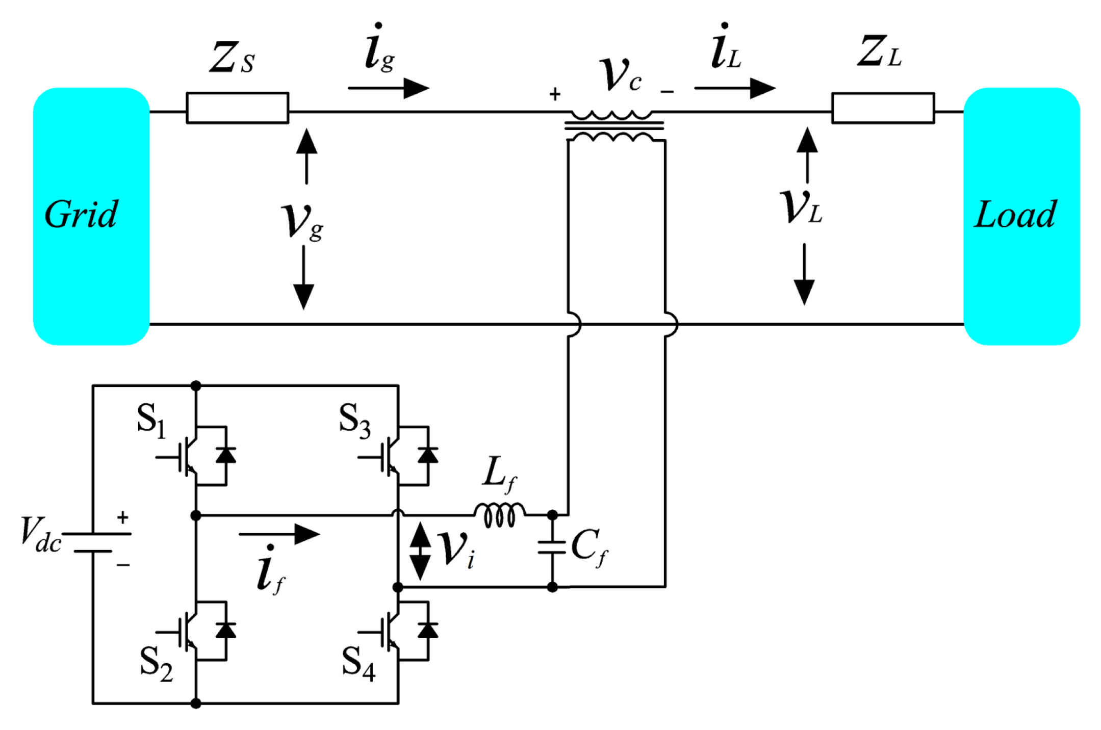
In this study, we consider a single-phase DVR. A connection diagram of the DVR is given in Figure 1. In this configuration, the DVR, which is a full-bridge voltage source inverter, is connected in series through a transformer to the protected load. Isolation between the load the DVR is provided by the transformer. Grid voltage sensor is used to continuously monitor the deviation from the reference voltage, and the appropriate compensation voltage is injected by the DVR to maintain the ideal voltage at the protected load terminal. Filter current and compensation voltage dynamics of the DVR are given by the following:
where , , , , , , and denote the input voltage by the DVR, grid voltage, compensation voltage, filter current, filter inductance, and filter capacitance, respectively. The DVR voltage can be expressed as where the DC-link voltage is denoted by , and the control signal is given by u. Moreover, in the ideal case, one can also write the following.
In normal operating condition, the compensation voltage given by (3) will be zero. However, in practice, the grid voltage is never ideal. Various grid anomalies such as voltage sag/swell, harmonics, noise, etc., are present. In this case, (3) can no longer be used for the compensation voltage calculation. In order to ensure that the sensitive load voltage remains as close as possible to the desired voltage, reference voltage needs to be calculated and this voltage should be in-phase with the grid voltage fundamental for the efficient operation by the DVR. Let us consider that the reference voltage is denoted by . Then, the tracking error and its derivative are given by the following.
Then, by substituting the DVR dynamical Equations (1) and (2) into (4) and (5), the DVR tracking error dynamics can be obtained as follows:
where the coefficient and the perturbation term is given by the following.
It is assumed that the perturbation term has a bounded derivative and is upper bounded by . Thus, the control of DVR is essentially divided into two parts. In part 1, the problem is to generate the reference voltage from the measured grid voltage . In part 2, the problem is to find the control signal u that will ensure that the tracking errors converge asymptotically to zero. These two issues are addressed in the following two sections.
3. Reference Signal Generator
In this Section, reference voltage will be generated from the measured grid voltage . For this purpose, let us consider the singe-phase grid voltage signal model in time-domain as provided below:
where , , and are the DC offset, amplitude, and instantaneous phase with being the grid frequency, and is the initial phase angle. The frequency is , where is the nominal frequency and is the deviation from the nominal frequency. For efficient operation of the DVR, the reference voltage should be in phase with the instantaneous phase of the grid voltage . Thus, the process of extracting from the measured voltage is considered in this section. For this purpose, a PLL-based approach has been considered in this study. Details are provided below.
3.1. DC Offset Rejection
Measurement offset causes estimation error in the estimated phase. Thus, rejection of this offset is essential in order to eliminate the steady-state error. For this purpose, the half-cycle delayed signal cancellation (DSC) method is a popular choice in the literature [34,35]. The same approach is considered here. For this purpose, let us consider half-cycle delayed version of the signal as follows:
where with being the period of the grid voltage signal. Then, the DC offset can be eliminated by the following operation.
In implementing Equation (10), the actual period of the grid voltage is required. In the off-nominal frequency condition, the amount of required dely could be a fraction, thereby increasing computational complexity. A potential solution is to use the nominal period; however, this will introduce amplitude and phase attenuation in the off-nominal condition. In this study, only extracting the phase is required. thus, appropriate compensation of the phase delay is necessary to eliminate the error. For this purpose, let us consider the transfer function of the DSC operation (10) as provided by the following:
where the estimated value is indicated by . The discrete-time version of the transfer function (11) is given by the following:
where the required delay is given by as with being the sampling frequency. By substituting , the phase angle of the transfer function (11) is given by the following.
3.2. Tuning-Free Fixed-Frequency Orthogonal Signal Generator
Once the DC offset is eliminated, the signal can be used to generate an orthogonal signal component. In this study, we are considering an all-pass filter (APF) [26,36]. APF is a first-order filter, and it can be used to generate orthogonal signals without any tuning gain. This filter can be used either as frequency-adaptive or non-adaptive configurations. In this study, a frequency-fixed operation is considered same as the DC offset rejection method, as highlighted in Section 3.1. The frequency-fixed APF transfer function is given by the following:
where superscript ⊥ indicates orthogonal signals. A time-domain block diagram of APF is provided in Figure 2. Similarly to Section 3.1, the frequency-fixed operation of the APF will introduce amplitude and phase attenuation in the estimated orthogonal signal. As such, characterization of the APF is needed to determine the necessary compensation mechanism. Phase-angle of the transfer function (14) is given by the following.
For small frequency drift, i.e., , it can be assumed that . Then, the phase angle (15) can be approximated as follows.
By ignoring the high-order ( and above) terms from the Taylor series expansion in (16), this equation can be simplified as follows.
As shown in (17), the first two terms are frequency independent while the third term depends on frequency variation. This term, i.e., , needs to compensated.
It is well known that single-phase grid voltage can be represented by an unbalanced two phase-system. It was shown in [36] that single-stage frequency-fixed APF cannot effectively remove the unbalanced component as the bandwidth of the unbalanced component rejection part is very narrow. As such, the unbalanced component will appear as double the fundamental frequency component after Park transformation. Thus, in order to eliminate this error, the double frequency component needs to be rejected. This issue can be solved by increasing the bandwidth of the notch component. In the literature, a two-stage APF has been suggested for this purpose. The two-stage APF effectively increases notch bandwidth and enables frequency-fixed APFs to reject off-nominal frequency unbalanced components. However, the two-stage APF will double the phase delay in the off-nominal frequency condition. As such, the required phase compensation value is computed by .
3.3. Implementation in PLL
The previous two subsections detailed the procedure for obtaining DC offset eliminated signal and its orthogonal component . These signals can be used as the input to PLL. The overall block diagram of the proposed PLL is provided in Figure 3. This section details the operating principle of this PLL. Before describing the phase detector operation of this PLL in our case, let us consider APF-filtered signals in the steady-state:
where is the off-nominal frequency phase attenuation by each stage of the APF. As per Figure 3, using the signal and , is obtained as follows.
The phase detector of the considered PLL is provided by the following.
Then, direct-axis and quadrature-axis voltages can be obtained directly from (21). By applying a quasi-locked condition, i.e., , the direct-axis and quadrature-axis voltages can be rewritten as follows.
Double frequency components in (22) and (23) can easily be filtered by applying moving average filter (MAF) with half-cycle window length. The transfer functions of MAF in continuous and discrete domain are provided by the following.
By applying MAF to (22) and (23) and also assuming negligible off-nominal frequency phase shift, filtered and can be approximated as follows.
Filtered voltages are then fed to the loop-filter of QT1-PLL, as shown in Figure 3.
3.4. Small-Signal Modeling and Tuning
A small-signal model of the proposed PLL can be obtained by considering the signal flow in Figure 3. For this purpose, first, the small-signal model of the pre-loop filters needs to be developed. The first pre-loop filter is the delayed signal cancellation block, which is given by transfer function (11). This transfer function can be converted into synchronous reference frame by substituting .
The transfer function of the APF in synchronous reference frame can be obtained by applying the Park transformation to single-stage APF and is given by the following Gautam et al. [26].
In our study, a two-stage APF is considered. As such, the effective transfer function is given by the following.
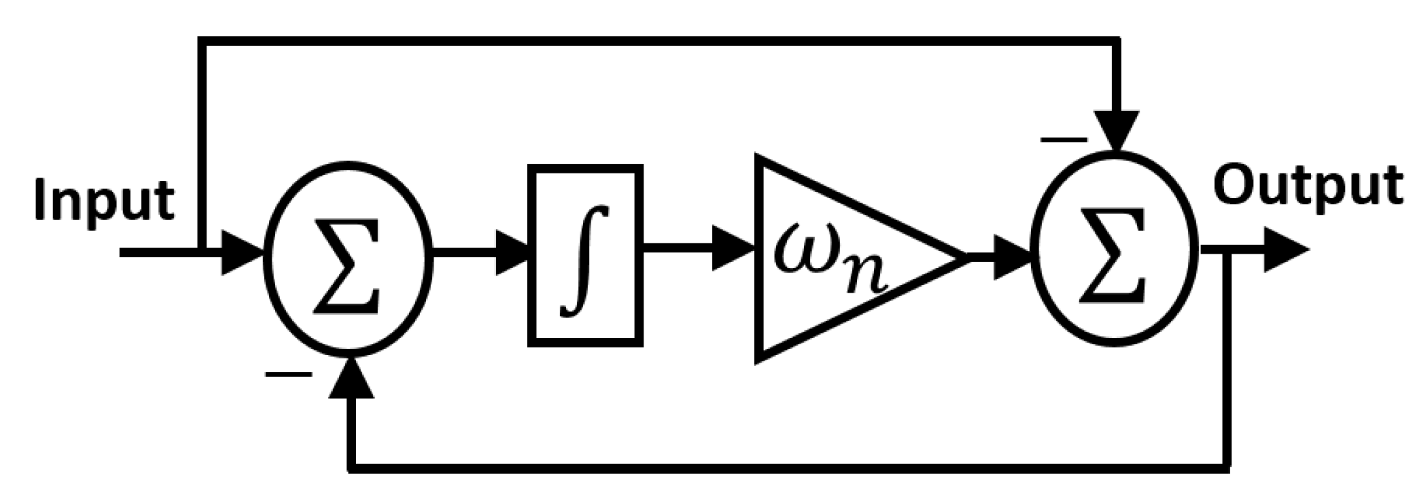
Considering the pre-loop filters, the small-signal model is shown in Figure 4, where is the overall phase compensation gain.
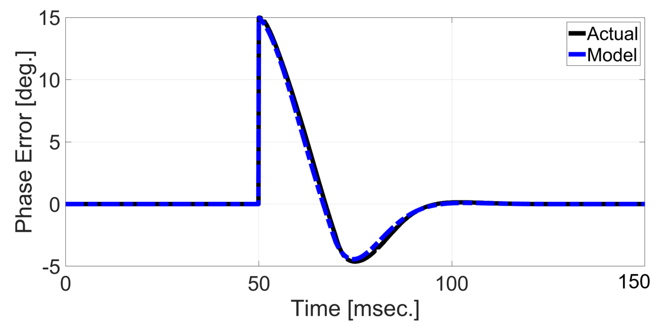
The proposed PLL has only one parameter to tune, which is the frequency estimation gain . This gain can be tuned in several ways. Two of the popular approaches are based on open-loop phase margin and settling time. The later is considered in this study. In order to tune gain using this method, a frequency step is considered. Considering a settling time, settling time versus the gain is given in Figure 5. From this figure, has been found to provide the fastest settling time. This value has been considered as the optimal gain for . Considering this value of validation of the small-signal model is provided in Figure 6.
Once the phase of the grid voltage fundamental component is estimated, the reference compensation voltage can be calculated as follows:
where reference magnitude is provided by . The design of the control signal u based on the reference grid voltage (31) is detailed in the next section.
4. Super Twisting Sliding Mode Controller Design
In this Section, tracking error dynamics (6) and (7) will be used for the control design. For this purpose, let us consider that the control signal is composed of , where is the nominal control signal and is the nonlinear part of the control signal. If we consider and , then the total control signal can be written as follows.
Tracking error dynamics (33) and (34) can be viewed as a perturbed second-order integrator. Numerous control techniques can be employed to stabilize the error under the presence of perturbation In this study, we consider a second-order SMC [31,37] in the form of super-twisting SMC [38]. In order to design the super-twisting SMC, let us consider the following sliding surface.
Then, the controller in (34) can be designed as follows:
where is the conventional signum function and the gains and are selected as follows.
In order to analyze the stability of the controller (36), let us consider the derivative of the sliding surface (35) together with (33), (34), and (36) as provided below.
Let us consider the following variables.
Then, for the selected control gain (37), finite-time convergence of the variables and can easily be established by using the results presented in Levant [37]. In order to implement the super-twisting controller, (32), (35), and (36) are required. An implementation block diagram of the super-twisting sliding-mode controller is provided in Figure 7.
5. Simulation and Experimental Results
In this Section, simulation and experimental results are reported. The experimental setup used in this study is demonstrated in Figure 8. Here, a Texas Instrument C2000 series micro-controller is used to implement the proposed control and estimation algorithm. Parameters of the setup and control gains are provided in Table 1.
Numerical simulation using Matlab/Simulink is conducted by considering the same values.
In the first test, the grid voltage suddenly experiences a ≈30% sag. From approximately 170 V (peak), the grid voltage dropped to roughly 120 V (peak). Experimental results are provided in Figure 9. The results show that in order to mitigate the effect of grid voltage sag at the sensitive load side, the DVR was very quick to react and supplied the necessary 50 V in-phase compensation voltage. As a result, constant voltage was maintained at the load side. In the second test, voltage swell was considered, and the results are provided in Figure 10. Here, grid voltage increased to 210 V, which is roughly a change from the nominal value. Unlike the first test, here, out-of-phase compensation voltage needs to be generated in order to reduce the voltage at the sensitive load end. As shown in Figure 10, the proposed enhanced QT1-PLL was very successful in generating the required roughly 40 V out-of-phase compensation voltage, and the sliding mode controller ensured the tracking of the reference compensation voltage by the DVR. These results show that the proposed approach can handle both sag and swell conditions. In the real grid, in addition to voltage sag/swell, harmonics are also a problem. The presence of harmonics will render the sensitive load voltage distorted. As a result, power quality degrades. In order to mitigate this issue, harmonic compensation is also required. In the final test, the grid voltage suddenly became distorted, and the results are provided in Figure 11. The proposed PLL can extract the fundamental component with high harmonic robustness. As a result, quick estimation of the grid harmonics was performed by PLL, and DVR injected the necessary harmonic compensation voltage to ensure very low distortion at the load side. The results in Figure 11 validate the suitability of the proposed PLL in a distorted grid condition.
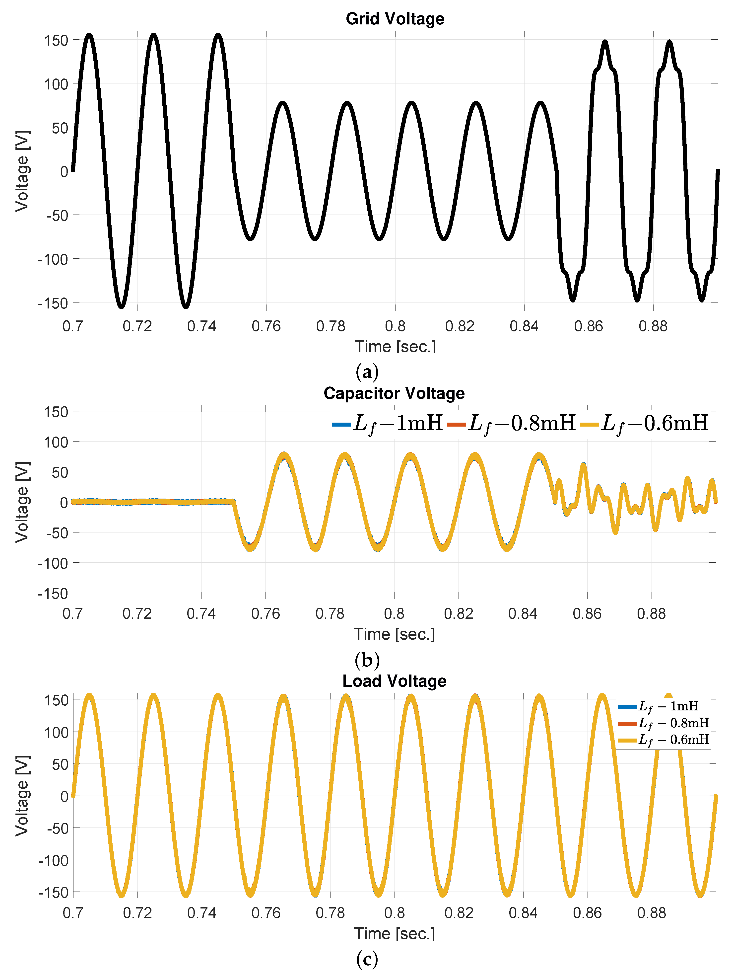
In order to check the robustness of the used controller, we have used numerical simulations. In the simulation test, voltage sag and harmonics are considered. The nominal value of the filter inductor is mH. This value is used to synthesize the control law. Simulation results with variation in the filter inductor are provided in Figure 12. The results in Figure 12 show that the response of DVR is very similar when the system parameter experienced a change from the nominal value. This shows that the sliding mode controller is robust to parameter variations.
Experimental results as shown in Figure 9, Figure 10 and Figure 11 independently considered voltage sag, swell, and harmonics. In practice, in addition to these characteristics, phase and/or frequency of the grid voltage may also change simultaneously in the worst case scenario. In order to asses the performance of the proposed method, two additional simulation studies were considered. In the first test, grid voltage experienced sag and phase change simultaneously. In the second test, in addition to the sag, the grid voltage also experienced + phase change and + frequency change. In both cases, the fault cleared after and the grid became distorted after fault clearance. Numerical simulation results for the first and second test are provided in Figure 13 and Figure 14. Results show that the proposed control method is very fast (roughly 1 cycle convergence time) despite very abrupt changes in grid voltage parameters. However, it is to be noted here that the load voltage transients are not that smooth compared to the case when only one parameter changed, such as in Figure 12. Smooth transient load voltage scan be obtained by either freezing the PLL or by using a very slow one [17]. However, this type of solution will not be able to provide efficient harmonic compensation. As such, a trade-off between the dynamic response and smooth transient behavior has to be made in PLL parameter selection.
6. Conclusions
In this paper, an enhanced single-phase quasi type-1 PLL was proposed to generate the reference compensation voltage for the multi-functional operation of a single-phase dynamic voltage restorer. A super-twisting sliding-mode controller was also proposed to track the reference voltage. The developed PLL is highly robust to grid voltage harmonics, which resulted in very low total harmonic distortion at the sensitive load-side. Moreover, thanks to a super-twisting controller, fast tracking of the compensation voltage was also achieved. Stability analysis and tuning of the PLL are presented by using small-signal modeling. The developed control method has been validated in a laboratory-scale prototype. The experimental results show that the proposed controller is very effective in compensating any grid voltage abnormalities, which in turn contributes to keeping the voltage at the sensitive load-side to remain very close to the ideal reference voltage.
Author Contributions
Conceptualization, H.A., S.B., H.K. and M.B.; methodology, H.A.; software, H.A. and S.B.; validation, S.B.; writing—original draft preparation, H.A.; writing—review and editing, H.A., S.B., H.K. and M.B. All authors have read and agreed to the published version of the manuscript.
Funding
H. Ahmed is funded through the Sêr Cymru programme by Welsh European Funding Office (WEFO) under the European Regional Development Fund (ERDF).
Institutional Review Board Statement
Not applicable.
Informed Consent Statement
Not applicable.
Conflicts of Interest
The authors declare no conflict of interest.
References
- Moghassemi, A.; Padmanaban, S. Dynamic voltage restorer (DVR): A comprehensive review of topologies, power converters, control methods, and modified configurations. Energies 2020, 13, 4152. [Google Scholar] [CrossRef]
- Yáñez-Campos, S.C.; Cerda-Villafaña, G.; Lozano-García, J.M. A Two-Grid Interline Dynamic Voltage Restorer Based on Two Three-Phase Input Matrix Converters. Appl. Sci. 2021, 11, 561. [Google Scholar] [CrossRef]
- Abas, N.; Dilshad, S.; Khalid, A.; Saleem, M.S.; Khan, N. Power quality improvement using dynamic voltage restorer. IEEE Access 2020, 8, 164325–164339. [Google Scholar] [CrossRef]
- Toumi, T.; Allali, A.; Abdelkhalek, O.; Abdelkader, A.B.; Meftouhi, A.; Soumeur, M.A. PV Integrated single-phase dynamic voltage restorer for sag voltage, voltage fluctuations and harmonics compensation. Int. J. Power Electron. Drive Syst. 2020, 11, 547. [Google Scholar] [CrossRef] [Green Version]
- IEEE Standard 1346-1998; IEEE Recommended Practice for Evaluating Electric Power System Compatibility with Electronic Process Equipment. IEEE: Piscataway Township, NJ, USA, 1998. [CrossRef]
- Lucas, A. Single-phase PV power injection limit due to voltage unbalances applied to an urban reference network using real-time simulation. Appl. Sci. 2018, 8, 1333. [Google Scholar] [CrossRef] [Green Version]
- Trabelsi, M.; Komurcugil, H.; Refaat, S.S.; Abu-Rub, H. Model predictive control of packed U cells based transformerless single-phase dynamic voltage restorer. In Proceedings of the 2018 IEEE International Conference on Industrial Technology (ICIT), Lyon, France, 20–22 February 2018; pp. 1926–1931. [Google Scholar]
- Kumar, C.; Mishra, M.K. Predictive voltage control of transformerless dynamic voltage restorer. IEEE Trans. Ind. Electron. 2015, 62, 2693–2697. [Google Scholar] [CrossRef]
- Ahmed, H.; Salgado, I.; Chairez, I.; Benbouzid, M. Robust gradient estimator for unknown frequency estimation in noisy environment: Application to grid-synchronization. IEEE Access 2020, 8, 70693–70702. [Google Scholar] [CrossRef]
- Ahmed, H.; Biricik, S.; Benbouzid, M. Enhanced Frequency Adaptive Demodulation Technique For Grid-Connected Converters. IEEE Trans. Ind. Electron. 2021, 68, 11053–11062. [Google Scholar] [CrossRef]
- Remya, V.; Parthiban, P.; Ansal, V.; Nandakumar, A. Single-phase DVR with semi-Z-source inverter for power distribution network. Arab. J. Sci. Eng. 2018, 43, 3135–3149. [Google Scholar] [CrossRef]
- Satputaley, R.J.; Borghate, V.B. Performance analysis of DVR using “new reduced component” multilevel inverter. Int. Trans. Electr. Energy Syst. 2017, 27, e2288. [Google Scholar] [CrossRef]
- Ahmed, H.; Biricik, S.; Benbouzid, M. Linear Kalman Filter-Based Grid Synchronization Technique: An Alternative Implementation. IEEE Trans. Ind. Inform. 2021, 17, 3847–3856. [Google Scholar] [CrossRef]
- Ahmed, H.; Benbouzid, M. Simplified Second-Order Generalized Integrator - Frequency-Locked Loop. Adv. Electr. Electron. Eng. 2019, 17, 405–412. [Google Scholar] [CrossRef]
- Ahmed, H.; Pay, M.L.; Benbouzid, M.; Amirat, Y.; Elbouchikhi, E. Hybrid estimator-based harmonic robust grid synchronization technique. Electr. Power Syst. Res. 2019, 177, 106013. [Google Scholar] [CrossRef]
- Meena, A.; Islam, S.; Anand, S.; Sonawane, Y.; Tungare, S. Design and control of single-phase dynamic voltage restorer. Sādhanā 2017, 42, 1363–1375. [Google Scholar] [CrossRef]
- Nielsen, J.G.; Newman, M.; Nielsen, H.; Blaabjerg, F. Control and testing of a dynamic voltage restorer (DVR) at medium voltage level. IEEE Trans. Power Electron. 2004, 19, 806–813. [Google Scholar] [CrossRef]
- Biricik, S.; Komurcugil, H. Optimized sliding mode control to maximize existence region for single-phase dynamic voltage restorers. IEEE Trans. Ind. Inform. 2016, 12, 1486–1497. [Google Scholar] [CrossRef]
- Biricik, S.; Khadem, S.K.; Redif, S.; Basu, M. Voltage distortion mitigation in a distributed generation-integrated weak utility network via a self-tuning filter-based dynamic voltage restorer. Electr. Eng. 2018, 100, 1857–1867. [Google Scholar] [CrossRef] [Green Version]
- Biricik, S.; Redif, S.; Özerdem, Ö.C.; Khadem, S.K.; Basu, M. Real-time control of shunt active power filter under distorted grid voltage and unbalanced load condition using self-tuning filter. IET Power Electron. 2014, 7, 1895–1905. [Google Scholar] [CrossRef] [Green Version]
- Rajkumar, K.; Parthiban, P. Grid voltage detection method based on a novel adaptive notch filter for control of transformerless dynamic voltage restorer. In Proceedings of the 2020 IEEE First International Conference on Smart Technologies for Power, Energy and Control (STPEC), Nagpur, India, 25–26 September 2020; pp. 1–6. [Google Scholar]
- Mellouli, M.S.; Hamouda, M.; Slama, J.B.H.; Al Haddad, K. A Third-order MAF Based QT1-PLL That is Robust against Harmonically Distorted Grid Voltage with Frequency Deviation. IEEE Trans. Energy Convers. 2021, 36, 1600–1613. [Google Scholar] [CrossRef]
- Golestan, S.; Freijedo, F.D.; Vidal, A.; Guerrero, J.M.; Doval-Gandoy, J. A quasi-type-1 phase-locked loop structure. IEEE Trans. Power Electron. 2014, 29, 6264–6270. [Google Scholar] [CrossRef] [Green Version]
- Ahmed, H.; Tir, Z.; Verma, A.K.; Ben Elghali, S.; Benbouzid, M. Quasi Type-1 PLL With Tunable Phase Detector for Unbalanced and Distorted Three-Phase Grid. IEEE Trans. Energy Convers. 2021. [Google Scholar] [CrossRef]
- Wu, C.; Xiong, X.; Taul, M.G.; Blaabjerg, F. On the Equilibrium Points in Three-Phase PLL Based on the d-axis Voltage Normalization. IEEE Trans. Power Electron. 2021, 36, 12146–12150. [Google Scholar] [CrossRef]
- Gautam, S.; Xiao, W.; Lu, D.D.C.; Ahmed, H.; Guerrero, J.M. Development of Frequency-Fixed All-Pass Filter based Single-Phase Phase-Locked Loop. IEEE J. Emerg. Sel. Top. Power Electron. 2021. [Google Scholar] [CrossRef]
- Ahmed, H.; Benbouzid, M. On the enhancement of generalized integrator-based adaptive filter dynamic tuning range. IEEE Trans. Instrum. Meas. 2020, 69, 7449–7457. [Google Scholar] [CrossRef]
- Golestan, S.; Guerrero, J.M.; Vasquez, J.C. Single-Phase PLLs: A Review of Recent Advances. IEEE Trans. Power Electron. 2017, 32, 9013–9030. [Google Scholar] [CrossRef]
- Omar, A.I.; Aleem, S.H.A.; El-Zahab, E.E.; Algablawy, M.; Ali, Z.M. An improved approach for robust control of dynamic voltage restorer and power quality enhancement using grasshopper optimization algorithm. ISA Trans. 2019, 95, 110–129. [Google Scholar] [CrossRef]
- Li, Y.W.; Blaabjerg, F.; Vilathgamuwa, D.M.; Loh, P.C. Design and comparison of high performance stationary-frame controllers for DVR implementation. IEEE Trans. Power Electron. 2007, 22, 602–612. [Google Scholar] [CrossRef]
- Komurcugil, H.; Biricik, S.; Bayhan, S.; Zhang, Z. Sliding Mode Control: Overview of Its Applications in Power Converters. IEEE Ind. Electron. Mag. 2021, 15, 40–49. [Google Scholar] [CrossRef]
- Biricik, S.; Komurcugil, H.; Ahmed, H.; Babaei, E. Super twisting sliding mode control of DVR with frequency-adaptive Brockett oscillator. IEEE Trans. Ind. Electron. 2021, 68, 10730–10739. [Google Scholar] [CrossRef]
- Biricik, S.; Komurcugil, H.; Tuyen, N.D.; Basu, M. Protection of Sensitive Loads Using Sliding Mode Controlled Three-Phase DVR With Adaptive Notch Filter. IEEE Trans. Ind. Electron. 2019, 66, 5465–5475. [Google Scholar] [CrossRef]
- Chedjara, Z.; Massoum, A.; Wira, P.; Safa, A.; Gouichiche, A. A fast and robust reference current generation algorithm for three-phase shunt active power filter. Int. J. Power Electron. Drive Syst. 2021, 12, 121–129. [Google Scholar] [CrossRef]
- Sevilmiş, F.; Karaca, H. A fast hybrid PLL with an adaptive all-pass filter under abnormal grid conditions. Electr. Power Syst. Res. 2020, 184, 106303. [Google Scholar] [CrossRef]
- Ramezani, M.; Golestan, S.; Li, S. Non-frequency sensitive all-pass filter based single-phase PLLs. In Proceedings of the 2016 IEEE/PES Transmission and Distribution Conference and Exposition (T&D), Dallas, TX, USA, 3–5 May 2016; pp. 1–5. [Google Scholar]
- Levant, A. Higher-order sliding modes, differentiation and output-feedback control. Int. J. Control 2003, 76, 924–941. [Google Scholar] [CrossRef]
- Derafa, L.; Benallegue, A.; Fridman, L. Super twisting control algorithm for the attitude tracking of a four rotors UAV. J. Frankl. Inst. 2012, 349, 685–699. [Google Scholar] [CrossRef]
Figure 1.
Topology of the considered DVR.

Figure 2.
Time-domain implementation of frequency-fixed APF.

Figure 3.
Overall block diagram of the proposed PLL.

Figure 4.
Small-signal model of the proposed PLL.

Figure 5.
Settling time versus for a frequency step change.

Figure 6.
Small-signal model verification of the proposed PLL with .

Figure 7.
Block diagram of super-twisting sliding-mode controller with and .

Figure 8.
Experimental setup used in this study.

Figure 9.
Experimental responses of , and subject to voltage sag in the grid.

Figure 10.
Experimental responses of , and subject to voltage swell in the grid.

Figure 11.
Experimental responses of , and subject to voltage harmonics in the grid.

Figure 12.
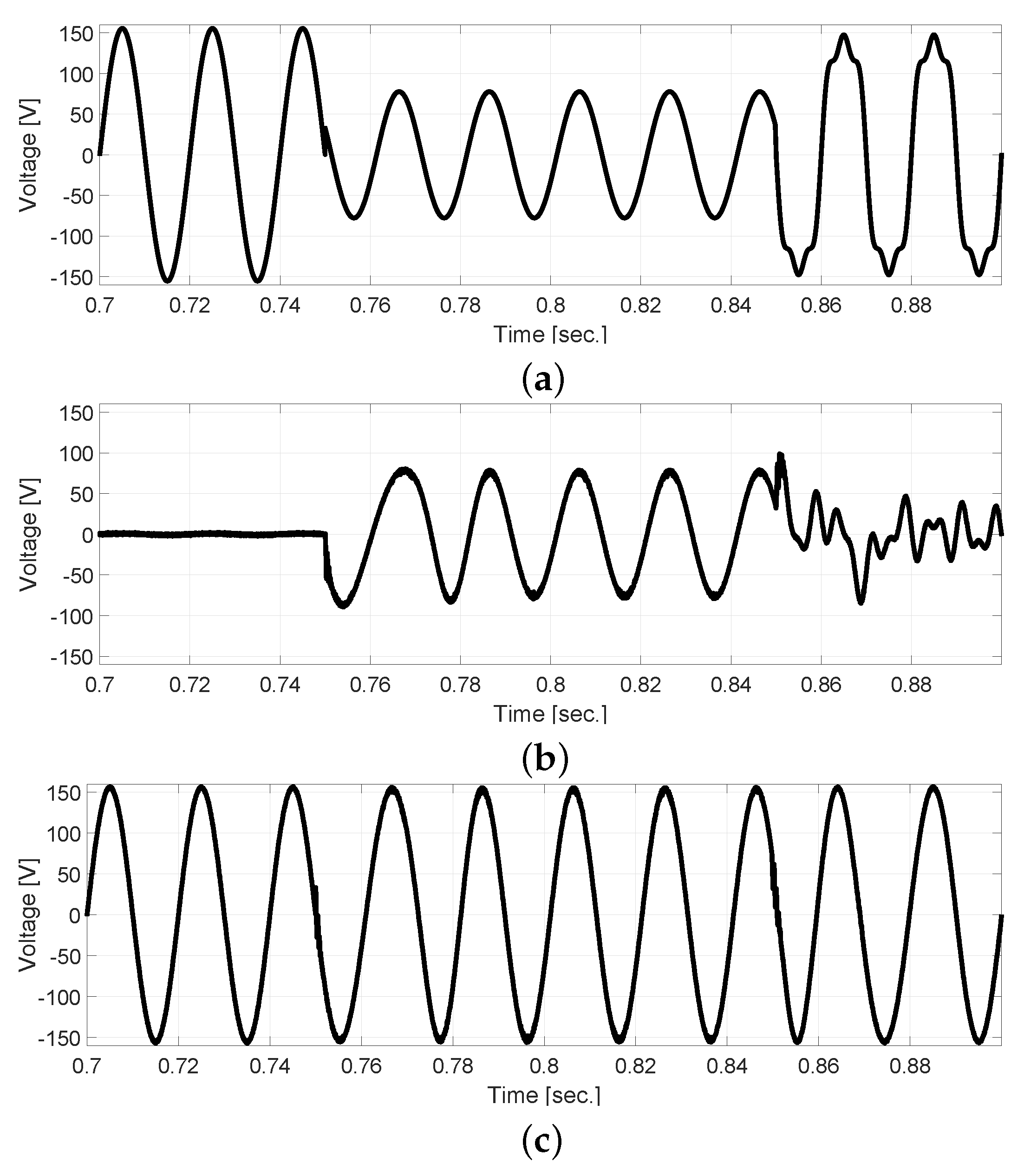
Simulation results for controller robustness check. (a) Grid voltage; (b) capacitor voltage; (c) load voltage.
Figure 12.
Simulation results for controller robustness check. (a) Grid voltage; (b) capacitor voltage; (c) load voltage.

Figure 13.
Simulation results for combined voltage sag and phase change at the grid. (a) Grid voltage; (b) capacitor voltage; (c) load voltage.
Figure 13.
Simulation results for combined voltage sag and phase change at the grid. (a) Grid voltage; (b) capacitor voltage; (c) load voltage.

Figure 14.
Simulation results for combined voltage sag, frequency, and phase change at the grid. (a) Grid voltage; (b) capacitor voltage; (c) load voltage.
Figure 14.
Simulation results for combined voltage sag, frequency, and phase change at the grid. (a) Grid voltage; (b) capacitor voltage; (c) load voltage.


Table 1.
Experimental study parameters.
| System and Control Parameters | Values |
|---|---|
| Controller gains | |
| PLL gain | |
| Grid: voltage and frequency | 120 V |
| Grid: impedance | , |
| Transformer turns ratio | 1:1 |
| DC link voltage, | 120 V |
| LC filter | , |
| Sensitive series load |
Publisher’s Note: MDPI stays neutral with regard to jurisdictional claims in published maps and institutional affiliations. |
© 2021 by the authors. Licensee MDPI, Basel, Switzerland. This article is an open access article distributed under the terms and conditions of the Creative Commons Attribution (CC BY) license (https://creativecommons.org/licenses/by/4.0/).
Share and Cite
MDPI and ACS Style
Ahmed, H.; Biricik, S.; Komurcugil, H.; Benbouzid, M. Enhanced Quasi Type-1 PLL-Based Multi-Functional Control of Single-Phase Dynamic Voltage Restorer. Appl. Sci. 2022, 12, 146. https://0-doi-org.brum.beds.ac.uk/10.3390/app12010146
AMA Style
Ahmed H, Biricik S, Komurcugil H, Benbouzid M. Enhanced Quasi Type-1 PLL-Based Multi-Functional Control of Single-Phase Dynamic Voltage Restorer. Applied Sciences. 2022; 12(1):146. https://0-doi-org.brum.beds.ac.uk/10.3390/app12010146
Chicago/Turabian StyleAhmed, Hafiz, Samet Biricik, Hasan Komurcugil, and Mohamed Benbouzid. 2022. "Enhanced Quasi Type-1 PLL-Based Multi-Functional Control of Single-Phase Dynamic Voltage Restorer" Applied Sciences 12, no. 1: 146. https://0-doi-org.brum.beds.ac.uk/10.3390/app12010146
Note that from the first issue of 2016, this journal uses article numbers instead of page numbers. See further details here.