
Online Signature Verification Systems on a Low-Cost FPGA


1
Electrical, Electronic and Automation Engineering Department, Universitat Rovira i Virgili, Avda. Països Catalans 26, 43007 Tarragona, Spain
2
Electronics Engineering Department, Universitat Politècnica de Catalunya, Avda. Victor Balaguer 1, 08800 Vilanova i la Geltrú, Spain
*
Author to whom correspondence should be addressed.
Appl. Sci. 2022, 12(1), 378; https://0-doi-org.brum.beds.ac.uk/10.3390/app12010378
Submission received: 16 November 2021
/
Revised: 27 December 2021
/
Accepted: 29 December 2021
/
Published: 31 December 2021
(This article belongs to the Special Issue Biometric Identification Systems: Recent Advances and Future Directions)
Abstract
:This paper describes three different approaches for the implementation of an online signature verification system on a low-cost FPGA. The system is based on an algorithm, which operates on real numbers using the double-precision floating-point IEEE 754 format. The double-precision computations are replaced by simpler formats, without affecting the biometrics performance, in order to permit efficient implementations on low-cost FPGA families. The first approach is an embedded system based on MicroBlaze, a 32-bit soft-core microprocessor designed for Xilinx FPGAs, which can be configured by including a single-precision floating-point unit (FPU). The second implementation attaches a hardware accelerator to the embedded system to reduce the execution time on floating-point vectors. The last approach is a custom computing system, which is built from a large set of arithmetic circuits that replace the floating-point data with a more efficient representation based on fixed-point format. The latter system provides a very high runtime acceleration factor at the expense of using a large number of FPGA resources, a complex development cycle and no flexibility since it cannot be adapted to other biometric algorithms. By contrast, the first system provides just the opposite features, while the second approach is a mixed solution between both of them. The experimental results show that both the hardware accelerator and the custom computing system reduce the execution time by a factor ×7.6 and ×201 but increase the logic FPGA resources by a factor ×2.3 and ×5.2, respectively, in comparison with the MicroBlaze embedded system.
1. Introduction
A handwritten signature requires a conscious action by the user, and therefore, it is one of the most usual methods by which persons claim their identity verification and accept responsibility for a signed document. Nonetheless, handwritten signatures have certain disadvantages, which have hindered their widespread use as biometric verification. The main challenge is the large intra-class and small inter-class variability. Samples taken from the genuine user may have large variability in their shapes. In addition, trained forgery signatures carried out by impostors may look very similar to signatures from the genuine user. Online signatures provide advantages for automatic biometric verification due to the additional information obtained from the capturing device, an electronic pen on a touch screen. Capturing angle and pressure samples, along with the shape coordinates, provides additional information about signature dynamics that increases inter-class variability.
Biometric systems are typically developed on general-purpose microprocessors due to the development comfortability provided by programming languages and compilers. Implementation issues, such as power consumption, data format, processing speed, or memory requirements, are not generally considered since they are assumed to run on high-performance computers. In contrast, portable systems are generally based on low-cost embedded microprocessors featured by memory and computing limitations. In such cases, algorithm optimizations, hardware accelerators or custom computers can be explored to provide an efficient implementation.
Biometric algorithms are usually composed of a set of computing stages that are used not only in different biometric modalities but also in computer vision, cryptography, and other fields. The computational requirements at some stages may hinder their applicability for real-time systems on general-purpose microprocessors. In such cases, the acceleration of some calculations by using FPGAs is an interesting possibility. Most of the works related to accelerators on FPGAs focus on a particular computing stage, such as the simplified FFT (Fast Fourier Transform) presented in [1], SVM (Support Vector Machine) implementations in [2] or the three-dimensional DTW (Dynamic Time Warping) architecture shown in [3]. However, complete biometric systems accelerated on FPGAs are scarce due to the development effort that must be carried out for their implementation. The work presented in [4] describes a pyramid-pipeline architecture of a convolutional neural network on FPGA for speaker recognition, and a complete biometric speaker verification system was presented in [5]. Other examples are the hardware accelerator of cryptosystem for iris, presented in [6], and the iris identification system on FPGA based on hardware-software co-design [7]. Related work about online signature biometrics on FPGA is even more scarce. The FPGA role described in [8] is to act as a wireless slave, which is connected to a computer executing a very simple signature algorithm. The online signature verification system proposed in [9] is based on a hardware accelerator, which has been deprecated by the second system presented in this paper.
The paper is organized into six sections. The next section of the paper briefly describes the online signature verification algorithm, which is implemented in the presented systems. Section 3 starts describing the adopted replacements of the IEEE 754 double-precision format in order to efficiently implement the algorithm on a low-cost FPGA family. The section continues with an architecture overview of the three implemented systems, their main advantages and drawbacks. Section 4 shows a detailed explanation about the DTW stage implemented on these systems, not only because it vastly dominates the total execution time of the signature verification but also because it is widely adopted in other biometric modalities, such as speaker [10], electrocardiogram [11], iris [12], and many others. The experimental results obtained on the three systems are reported in Section 5. Finally, discussions are presented in the last section.
2. Signature Verification Algorithm
Signature biometric systems are usually based on two phases: enrollment and verification. At the enrollment phase, the system is trained for a genuine user who provides several signatures to extract a set of distinguishing features, which is stored as the user dataset. During the verification phase, a new signature is presented, and its features are extracted and matched against the previously stored one. Then, by computing a similarity score that is compared with a threshold value, the signature is classified as genuine or counterfeit.
Most online signature verification techniques can be classified as template, statistical or structural matching [13,14]. Template matching is a straightforward comparison of samples from the genuine user and the presented signature, which are usually pre-aligned by a DTW algorithm [15]. In statistical matching, the most salient behavioral signature features are compared and scored by means of a neural network, a hidden Markov model or a GMM (Gaussian Mixture Models). Structural matching is based on syntactic approaches for representing signatures that are compared through graph or tree techniques.
The signature verification algorithm consists of four stages: pre-processing, DTW, extraction of features and GMM matching, as depicted in Figure 1. The initial pre-processing applies a set of transformations on the captured signature, as resampling, centering and rotating the shape, and normalization. The resulting data are a set of 256-width vectors containing normalized samples. Then, a DTW algorithm computes the optimal alignment between the time-dependent samples of the processed signature and the enrolled template. Finally, a set of statistical features are extracted from the aligned signature, known as pseudo-distances, to execute a GMM model that calculates a distance score.
The dataset of an enrolled user on the implemented online signature system [16] is composed of a signature template and its GMM parameters. The signature template consists of 256-width vectors containing normalized samples (x-y coordinates, pressure, angles). A set of distinctive features from the signature are selected to generate a GMM model. The parameters of the optimal GMM model for each enrolled user are computed by the expectation-maximization (EM) algorithm [17] with a public signature database [18]. The database contains 25 genuine signatures and 25 skilled forgeries for 100 different users. Basically, the implemented algorithm is an improved version of the presented one [19] by adding dynamic features, such as speeds and accelerations, at the GMM matching.
The algorithm performance was tested by the public database available in [18]. The DET (Detection Error Tradeoff) curve, shown in Figure 2, represents the relationship between FMR (False Match Rate) and FNMR (False Non-Match Rate) for different threshold decision values [16,19]. The EER (Equal Error Rate) achieved by the proposed online signature algorithm is 2.74%, which is a competitive performance when compared to other biometric modalities presented in some competitions [20].
3. Hardware Implementations
This paper proposes the implementation of three different approaches for the signature verification system using an FPGA. The first one is an embedded system based on a 32-bit microprocessor, which includes a single-precision floating-point unit (FPU). In the second one, the FPU is substituted by a hardware accelerator especially designed for resolving calculations on floating-point vectors. The last one is a custom computing system built by means of a large set of fixed-point arithmetic circuits.
The algorithm was initially developed on MATLAB where, by default, real numbers are represented by IEEE 754 double-precision format. This standard is a 64-bit floating-point format, which provides both a large dynamic range of representable data and high resolution [21]. However, arithmetic circuits based on this format are significantly complex, and usually, only 64-bit high-performance processors include double-precision FPU. Therefore, to achieve high efficiency when the algorithm is implemented on low-cost FPGAs, the double-precision data must be replaced to simplify the arithmetic circuits but without affecting the biometric performance. Moreover, the format replacement also reduces the required capacity of the involved memories.
As mentioned, the systems based on the 32-bit embedded microprocessor require an IEEE 754 single-precision FPU or the hardware accelerator. However, the implementation of the customized system using the single-precision format is not practical due to the large number of required arithmetic circuits. The IEEE 754 arithmetic circuits require a large number of hardware resources and execution clock cycles due to denormalization, normalization and rounding steps that are not carried out on integer arithmetic circuits. Alternatively, real numbers can be represented by binary fixed-point formats, which are basically integers scaled by a constant factor. Consequently, the implementation of arithmetic circuits in such format is much simpler and faster than their floating-point counterparts. However, the number of bits in the fixed-point format must be properly adjusted to avoid overflow or underflow problems that would affect the algorithm performance.
As the algorithm includes several stages that require different ranges and precisions, a variable fixed-point format is chosen. Using the Q-format [22] and the notation Qmk.nk to represent a format, mk and nk stands for the number of bits for the integer and fractional parts, respectively. If K is the total number of computations involved in the whole algorithm, the mk and nk values in the k-th computation are selected according to the methodology shown in Figure 3. Note as mk can be easily calculated by logging the range of results to avoid overflow errors. On the other hand, nk is selected as the minimum value that does not provide excessive error due to lack of precision.
The algorithm is initially executed in double-precision and single-precision formats to record results and verify that both versions provide the same biometric performance. The final distance scores (rdouble-precision, rsingle-precision) are used to calculate the maximum error criterium for the fixed-point version. Then, the methodology continues executing the fixed-point version of the algorithm, obtaining mk from the logged results and incrementing nk until the distance score (rQm.n) meets the error criterium at each computation on the entire signature database, according to the following equation.
The fixed-point formats obtained range from the simpler Q10.0 format at the pressure samples acquisition to the largest Q7.45 format associated with the pseudo-distances. Table 1 shows the statistical analysis of the errors obtained from both algorithm versions on the database.
3.1. MicroBlaze Embedded System
Figure 4 shows an overview of the embedded system based on MicroBlaze, a 32-bit soft-core general-purpose microprocessor for Xilinx FPGAs. It can be configured to better fit the computational requirements with the possibility of providing a single-precision FPU to accelerate floating-point operations. In this approach, the algorithm is written in C programming language, and single-precision IEEE 754 format is used. The C compiler automatically translates floating-point code to FPU instructions, and, therefore, the implementation or modification of the algorithm is reduced to a programming problem. Consequently, this implementation provides the lowest development effort but the worst execution time when compared against the other alternatives. The flexibility of the system is very high since the hardware can be reused for other biometric algorithms.
3.2. Hardware Accelerator
The second approach attaches a hardware accelerator, named FPBA (Floating-Point Biometric Accelerator) [23], to the embedded system. The FPBA is a programmable accelerator designed to speed up operations on floating-point vectors, commonly used in several biometric algorithms. MicroBlaze configures the FPBA at runtime, setting pointer registers to the vectors stored on external memory and the floating-point instructions that must be executed. Then, the FPBA launches the instructions, automatically retrieving/writing vectors from/to memory when required through memory channels, independent of MicroBlaze. Starting from the first approach, the implementation of the algorithm is also reduced to a programming problem but replacing the C code that must be accelerated by FPBA instructions on floating-point vectors.
The FPBA is basically a programmable processor that controls a pipelined FPU attached to memory channels, improving the execution time of biometric algorithms on floating-point vectors. A vector is a set of sequentially ordered data, which is stored in the memory. Vector lengths are configurable, launching a set of FPBA instructions repeatedly in hardware-controlled loops. Partial results of a vector computation can be temporarily stored in the internal registers and can be retrieved when needed. Any FPBA instruction defines the operation type (MIN, ADD, SQRT, etc.) on the involved source and destination operators, which can be vectors (V0 to V7), registers (R0 to R15) or scalars (S0 to S7).
Figure 5 depicts an overview of the architecture, which is mainly focused on the fast execution of single-precision operations on vectors, commonly used in biometrics. Firstly, the pipelined FPU increases the throughput to one instruction per clock cycle of the most frequently used operations (as the maximum, addition/subtraction and multiplication). The throughput of more complex operations, such as the square root and exponential, is greatly decremented to one instruction per 28 clock cycles. Secondly, a register file temporarily stores partial results of operations that form a computation over vectorized data. Finally, the double control unit (CU0 and CU1) permits two sets of instructions virtually executed in parallel, multiplexing on time the driving of signals for the FPU and registers through an arbiter. The CU0 can continuously launch those instructions with the faster throughput; meanwhile, CU1 is waiting for the result from instructions with a slower throughput.
FPBA instructions should be properly ordered and grouped, reducing latencies due to operand dependencies. Moreover, instructions can also be separated to take profit of the double control unit, enhancing the execution time. This approach improves the execution time when compared with the previous embedded system, maintaining the flexibility of the hardware reusability for other biometrics. Nonetheless, it requires a deep knowledge of the FPBA architecture and timing details, and, therefore, a higher development effort when compared with the first approach.
3.3. Custom Computing System
The last implementation approach is a custom computing system, which does not require the MicroBlaze embedded processor, as depicted in Figure 6. The PicoBlaze, which is a very simple 8-bit microcontroller, is primarily used to trigger the starting of the verification and to retrieve the final score through an RS232 communication port, as well as for debugging tasks. All computations are carried out using a set of specialized arithmetic circuits that are provided with internal BRAM (Block RAM) memories to share data between them. The DTW circuit additionally requires external memory to store the large result matrix. The feature extraction circuit is embedded in the GMM circuit, and it permits the parallel computing of the pseudo-distances along the optimal warping path, in order to reduce the execution time.
4. DTW
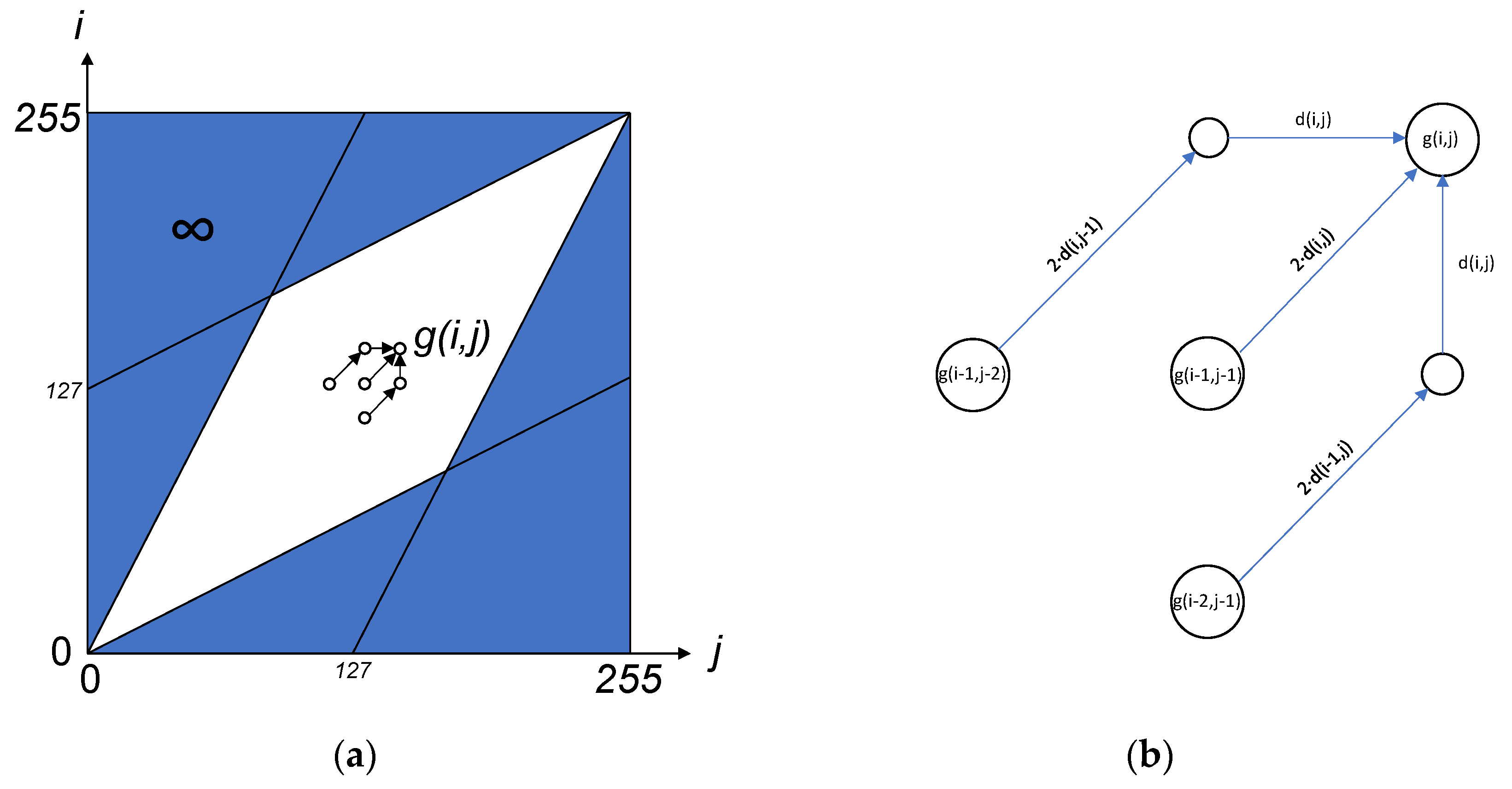
The DTW result is used to find the optimal time alignment between signals s and t by computing a G matrix, which is composed of points. The optimal warping path is the set of points with minimal , pairing each sample with another sample. Figure 7 shows the bidimensional DTW implemented in the signature algorithm, which aligns 256-width x-y samples from the acquired signature to the enrolled template . The DTW computes the result matrix G by pairing shape samples and on a permitted region R. Typically, DTW regions can be the Sakoe–Chiba band or the Itakura parallelogram [15,24], which is the one chosen in the work presented. The algorithm starts declaring the initial condition and continues computing each new on R, until the last is calculated.
The initial condition is declared at the point . Alignment outside the region is not permitted by declaring on the points that do not belong to R.
Each on R is selected as the minimum value of three possible paths, depending on both previously computed points of the G matrix and three distances.
The denotes the Euclidean distance between the bidimensional samples, which involves a square root operation.
In order to enhance the execution time of the DTW algorithm, all three approaches minimize the number of square root operations by an auxiliary matrix D, which is previously calculated. The distances required to calculate are retrieved from the D matrix, avoiding repeating the distance computation on the same point. Furthermore, the runtime of the DTW algorithm can be optimized by parallelizing the computations of the matrices D and G, which are adopted in the last two approaches. Finally, a high throughput square root calculation on the previous optimizations can greatly reduce the DTW execution time, as in the custom circuit approach.
4.1. MicroBlaze Embedded System
The next programming pseudo-C code shows the main details about the implementation of the algorithm on the MicroBlaze microprocessor. The G matrix will be computed only at the points belonging to the region R. Consequently, an initializing function writes , excepting at the starting point . In order to improve execution time, a distance D matrix is previously computed to avoid repeated computations of distances on the same point. The D matrix stores at points that belong to R, and required distances are retrieved from D during the G matrix computation. Each matrix is composed of 256 × 256 single-precision data, requiring 256 KB of storage capacity on external memory. As it is shown, matrices D and G are processed row by row, and each row is calculated by a set of operations on sequentially ordered data.

4.2. Hardware Accelerator
In the previous programming code, column data from the D and G matrices are sequentially allocated in external memory, as in floating-point vectors. Consequently, the FPBA can accelerate computations carried out on columns by launching a set of instructions. The throughput of all required instructions is one per clock cycle, except the square root instruction in the D matrix computation. The execution time on the FPBA is enhanced by the double control unit, which launches instructions for G and D matrices in a time-multiplexed way. Since G computation requires the previous calculus of D, the computation of the G matrix at row is virtually executed in parallel with the D matrix at the next row . For the sake of simplicity, the programming code for the first and last row is omitted as they are slightly different from the code shown.

The D matrix computation is performed by the following CU1 code, which consists of six instructions in a loop, generating iterations by controlling a k index, which starts at 0. The first instruction stores in register R14 the subtraction result from a scalar S5, which stores the sample, and a sample from the vector V5. The values are sequentially retrieved from memory according to , since the vector pointer was configured to start at the element. Similarly, another instruction stores in R15 the other required subtraction, and the following instructions complete the calculation. The last instruction stores the result sequentially on the V7 pointer, which was configured by MicroBlaze to the first element

In order to enhance the G matrix computation, the CU0 instructions are ordered to reduce latencies due to operand dependencies and grouped to calculate two consecutive and elements at each loop iteration. Consequently, the vector length was configured to and the last two instructions write and at each iteration in the V4 vector. The V0 and V1 vector pointers are set to the first required elements of D at the rows and , to read and , respectively. Similarly, V2 and V3 vectors point the first elements of G elements to be retrieved from memory, reading a new and at each iteration. After completing a set of multiplications and additions, instructions (*) in the following code store the three possible values in registers R4, R5, R6. Similarly, R9, R10, R11 are written with the possible values at (**). The last instructions choose the minimum values to be stored in , and write R0, R1 with the data required for the next iteration. Due to the fast throughput of these instructions, the CU0 launches many of them meanwhile CU1 is calculating the square root result.

4.3. Custom Computing System
The DTW computing circuit is a highly parallelized architecture able to simultaneously access several double-port internal BRAM memories, performing a throughput of one calculus per clock cycle after an initial latency. It is composed of two dedicated circuits built from fixed-point arithmetic circuits and a controller unit, as depicted in Figure 8 and Figure 9. The first circuit is devoted to the calculus of the D matrix at the next row , while the second circuit computes the G matrix on the current row , similarly as in the FPBA. The controller not only drives the multiplexers, demultiplexers and BRAMs at the computing circuits but also maintains a proper synchronization of both circuits and generates the required indexes for the region R. The region bounds , at the and rows are retrieved from two BRAM memories (acting a ROMs), generating the required range of indexes during the calculation of D and G at each row.
The D matrix circuit is quite simple. It devotes two BRAMs to retrieve the , , , samples and a few arithmetic fixed-point circuits to calculate the distances . The square root circuit is the CORDIC core from Xilinx’s LogiCORE [25], which is configured to enhance the performance by fully parallel architecture with a single-cycle data throughput. The core is able to calculate one square root per clock cycle in fixed-point format after an initial latency of 22 clock cycles. Distance results are temporarily stored in BRAMs instead of the external RAM, since only the previous two rows of D are required during the computation of a row of G. The double-port BRAMs allow to simultaneously store a new result and retrieve a previously calculated distance.
The G matrix circuit is significantly more complex. It devotes two BRAMs (da, db) and a set of multiplexers and demultiplexers to store the result and to retrieve the three distances , , in a single clock cycle, as required for the calculation of each . During a row computation, and are read from BRAM db, is retrieved from BRAM da, and meanwhile it stores the result . The roles of da and db are alternatively swapped on each new row calculation. Similarly, only two rows of G are required during the calculation, and two BRAMs simultaneously retrieve all the necessary data and store the result. During a row calculation, and are read from gb, is retrieved from ga meanwhile it stores the result . On each new row, the ga, gb roles are swapped, and a set of fixed-point arithmetic circuits calculate the result. The results are also written into the external memory since the following feature extraction stage requires the complete G matrix to compute the pseudo-distances on the optimal warping path.
5. Experimental Results
5.1. Speed Processing
The execution times, expressed in clock cycles, for the three implementations are experimentally obtained and shown in Table 2 at each of the stages of the algorithm. These results represent the average execution time obtained from all the available signatures of a single user. The execution times are not dependent on the presented signature, except a slight variation in the features extraction stage due to the different warping paths used to compute the pseudo-distances, which is negligible in the total execution time. Between brackets, the speed-up factors of the last two implementations are reported when compared with the embedded system. The table also shows the execution time in milliseconds at the clock frequencies used in the implemented systems, according to the synthesis results.
The total execution time is clearly dominated by the DTW stage since it requires both calculations on large matrices and square root operations. Experimental results show that the speed-up factors are ×7.6 and ×201 for the FPBA and custom system, respectively. The acceleration of the custom DTW circuit is very noticeable due to the high throughput achieved when calculating (one computation per clock cycle).
As stated in Section 1, there is a lack of online signature systems on FPGAs. However, we can compare the acceleration of the execution time of our custom DTW circuit against other DTW-based FPGA accelerators in Table 3. The 3D-DTW accelerator [3] for action recognition is designed to be connected to the ARM microprocessor embedded in the target Zynq-7000 device, a high-performance SoC from Xilinx. The core running at 100 MHz can accelerate the execution time ×40 times faster than the software counterpart. A closer comparison can be achieved with the 2D-DTW accelerator for embedded platforms [26]. As the previous accelerator, it is designed to be connected to an ARM microprocessor on a Cyclone V device from Altera, achieving a ×7.5 speed-up running at 60 MHz.
We compare the execution time of different DTW implementations since the result depends on several parameters. The dimension of samples affects the calculation of the distance, the sample width and region R determine the number of points to compute , and the data format affects the latency of the arithmetic circuits. Therefore, the cycle time of calculating is a better comparative measurement.
The core shown in [3] presents important differences when compared with the DTW algorithm implemented in this work. First, it does not compute the optimal warping path since it only requires the minimum value at the last row, which scores the similarity of the aligned samples. The algorithm is repeated in 12 different templates in order to classify the captured action. Moreover, each distance is calculated from the addition of 3 square root operations. Additionally, it does not use any specific region, calculating at all possible points. Finally, to improve the execution time, the DTW stops if the minimum value of at any point in a row is greater than a threshold condition. The execution time for 576-width floating-point samples ranges from 8.7 × 10⁶ to 11.6 × 10⁶ clock cycles at 100 MHz. The higher time should be considered since it calculates on all the points (331,776 points), providing a cycle time of 349 ns (34.9 clock cycles).
The DTW accelerator [26] is much closer to the proposed version used in this paper since it implements the Euclidean distance for 2D samples. However, the resolution of samples is limited to 8-bit, and it uses the Sakoe–Chiba region. The execution time for 250-width samples is 0.12 ms (7200 clock cycles) by computing only the 5% of the G matrix (3125 points) due to the parameters of the region. Therefore, the cycle time when calculating is about 38.4 ns (2.3 clock cycles).
The custom computing system works with 28-bit samples using a Q1.27 fixed-point format. The DTW execution time, for 256-width samples on an Itakura region that computes 33.3% of the G matrix (21,845 points), is 0.437 ms (21,870 clock cycles). Therefore, the cycle time of achieves 20.01 ns, which is very close to the theoretical one (1 clock cycle).
The FPBA is not specifically designed to calculate the DTW but rather to speed up several computing stages of biometric algorithms. Therefore, the performance is not as competitive as in the DTW accelerators. The 256-width samples are in 32-bit floating-point format, taking 15.8 ms to calculate the DTW in the same region as in the custom system. The cycle time is 723.28 ns (29.0 clock cycles).
5.2. FPGA Resources
The devoted FPGA hardware resources and clock frequency are obtained from the synthetized circuits on a XC3S2000 device and reported in Table 4. The incremented ratio of FPGA resources for the FPBA and the custom systems, when compared with the first implementation, are also reported in brackets. The FPBA is attached to the embedded system, and therefore, the logic resources are incremented. The custom computing system is built from a large set of dedicated arithmetic circuits and internal memories, significantly incrementing the number of FPGA resources needed. Mainly, the CLBs (Complex Logic Block), which mainly consists of LUTs (LookUp Table) and FFs (Flip-Flop), are incremented by factors ×2.3 and ×5.2 for the FPBA and the custom system, respectively. The clock frequency of the custom system is slightly increased due to the simplified architecture of the fixed-point arithmetic circuits.
6. Discussion
The paper presents three different approaches to implementing an online signature verification system on a low-cost FPGA family from Xilinx. Firstly, the IEEE 754 double-precision data were replaced by simpler formats without degrading the algorithm biometric performance. The simple-precision floating-point format is adequate for embedded systems based on the 32-bit microprocessor MicroBlaze configured with internal FPU. The same data format is used for the hardware FPBA, which accelerates floating-point computations on data vectors. An alternative representation of real numbers is the fixed-point format since arithmetic circuits are simpler and faster than their floating-point counterparts. This data format is used by the custom computing system, which is built from a large set of devoted arithmetic circuits.
Each of the three tested alternatives has its advantages and drawbacks. The MicroBlaze embedded system provides a simpler and faster development cycle since the compiler automatically translates single-precision operations to FPU instructions. The system provides a high flexibility because it could be adapted to different biometric algorithms by including a new programming code. Nonetheless, execution time is limited due to the floating-point operations on large data. The FPBA accelerates the processing time (×7.6) on floating-point vectors, also providing a high flexibility. However, the programming effort is increased since it is required to rewrite the code that must be accelerated as vector operations and write FPBA instructions properly. Another drawback is the increase in FPGA resources (×2.3). The last alternative is a custom computing system built from a large set of devoted fixed-point arithmetic circuits and internal BRAM memories. This proposal features the opposite advantages and drawbacks when compared to the embedded system, providing a very large acceleration (×201) but no system flexibility. Furthermore, the implementation area is noticeably incremented (×5.2), and the development effort is enormous due to the large set of customized computational circuits and memories that must be managed.
Depending on the target, one proposal is preferred against the others. Taking a multi-modal biometric system into perspective, a custom computing system could provide a very fast execution time at the expense of a huge increase in both the FPGA resources and development effort, which may not be justifiable. In such a case, the FPBA could be the preferred option since it allows accelerating the processing time without increasing the hardware resources, along with a reasonable development effort.
Author Contributions
All authors wrote and reviewed specific sections of the paper. E.C.N. focused on the algorithm porting to C and the FPBA system and experimental results. R.R.L. mainly contributed to the custom computing system and experimental results. M.L.G. mainly contributed to the MATLAB algorithm and optimizations. All authors have read and agreed to the published version of the manuscript.
Funding
This research was funded by Spanish MCIN/AEI/10.13039/501100011033, grant number PID2019-107274RB-I00.
Institutional Review Board Statement
Not applicable.
Informed Consent Statement
Not applicable.
Data Availability Statement
Not applicable.
Conflicts of Interest
The authors declare no conflict of interest.
References
- Reynoso-Godinez, R.; Rodriguez-Donate, C.; Lopez-Ramirez, M.; García-Guevara, F.M. FPGA-based parallel process for Walsh-Hadamard transform. Electron. Lett. 2020, 56, 1039–1041. [Google Scholar] [CrossRef]
- Afifi, S.; GholamHosseini, H.; Sinha, R. FPGA Implementations of SVM Classifiers: A Review. SN Comput. Sci. 2020, 1, 133. [Google Scholar] [CrossRef] [Green Version]
- Vidhaypathi, C.M.; Raj, J.; Noel, A.; Sundar, S. The 3D-DTW Custom IP based FPGA Hardware Acceleration for Action Recognition. J. Imaging Sci. Technol. 2021, 65, 10401-1–10401-10. [Google Scholar] [CrossRef]
- Xu, J.; Li, S.; Jiang, J.; Dou, Y. A Simplified Speaker Recognition System Based on FPGA Platform. IEEE Access 2019, 8, 1507–1516. [Google Scholar] [CrossRef]
- Ramos-Lara, R.; López-García, M.; Cantó-Navarro, E.; Puente-Rodriguez, L. Real-Time Speaker Verification System Implemented on Reconfigurable Hardware. J. Signal Process. Syst. 2013, 71, 89–103. [Google Scholar] [CrossRef] [Green Version]
- McGuffey, C.; Liu, C.; Schuckers, S. Hardware Accelerator Approach Towards Efficient Biometric Cryptosystems for Network Security. J. Comput. Inf. Technol. 2015, 23, 329–340. [Google Scholar] [CrossRef]
- López, M.; Daugman, J.; Cantó, E. Hardware-software co-design of an iris recognition algorithm. IET Inf. Secur. 2011, 5, 60–68. [Google Scholar] [CrossRef] [Green Version]
- Sandeep, D.; Chandrakanth, C. Online Signature Verification by Using FPGA. Int. J. Mag. Technol. Manag. Res. 2017, 4, 372–377. [Google Scholar]
- López-García, M.; Ramos-Lara, R.; Miguel-Hurtado, O.; Cantó-Navarro, E. Embedded System for Biometric Online Signature Verification. IEEE Trans. Ind. Electron. 2014, 10, 491–501. [Google Scholar] [CrossRef]
- Mansour, A.H.; Salh, G.Z.A.; Mohammed, K.A. Voice Recognition using Dynamic Time Warping and Mel-Frequency Cepstral Coefficients Algorithms. Int. J. Comput. Appl. 2015, 116, 34–41. [Google Scholar] [CrossRef] [Green Version]
- Shen, Y.; Bao, S.; Yang, L.; Li, Y. The PLR-DTW method for ECG based biometric identification. In Proceedings of the 2011 Annual International Conference of the IEEE Engineering in Medicine and Biology Society, Boston, MA, USA, 30 August–3 September 2011. [Google Scholar]
- Bernadelli, C.R.; da Silva, P.R. Dynamic Time Warping in Iris Biometric Recognition Process. IEEE Lat. Am. Trans. 2021, 19, 42–49. [Google Scholar] [CrossRef]
- Impedovo, D.; Pirlo, G. Automatic signature verification: The State of the Art. IEEE Trans. Syst. Man Cybern. Part C Appl. Rev. 2008, 38, 609–635. [Google Scholar] [CrossRef] [Green Version]
- El-Henawy, I.; Rashad, M.; Nomir, O.; Ahmed, K. Online Signature Verification: State of the art. Int. J. Comput. Technol. 2005, 4, 664–678. [Google Scholar] [CrossRef] [Green Version]
- Sakoe, H.; Chiba, S. Dynamic programming algorithm optimization for speaker word recognition. IEEE Trans. Acoust. Speech Signal Process. 1978, 26, 43–49. [Google Scholar] [CrossRef] [Green Version]
- Miguel Hurtado, O. Online Signature Verification Algorithms and Development of Signature International Standards. Ph.D. Dissertation, Universidad Carlos III Madrid, Getafe, Spain, 2011. [Google Scholar]
- Dempster, A.P.; Laird, N.M.; Rubin, R.B. Maximum likelihood from incomplete data via the EM algorithm. J. R. Stat. Soc. Ser. B (Methodol.) 1977, 39, 1–22. [Google Scholar]
- Ortega, J.; Fierrez, J.; Simón, D.; González, J.; Faundez, M.; Espinosa, V.; Satue, A.; Hernaez, I.; Igarza, J.; Vavaracho, C.; et al. MCyT base corpus: A bimodal biometric database. IEE Proc. Vision Image Signal Process. 2003, 150, 395–401. [Google Scholar] [CrossRef] [Green Version]
- Miguel-Hurtado, O.; Mengibar-Pozo, L.; Pacut, A. A new algorithm for signature verification system based on DTW and GMM. In Proceedings of the 2008 42nd Annual IEEE International Carnahan Conference on Security Technology, Prague, Czech Republic, 13–16 October 2008; pp. 206–213. [Google Scholar] [CrossRef]
- Cappelli, R.; Ferrara, M.; Franco, A.; Maltoni, D. Fingerprint verification competition 2006. Biom. Technol. Today 2007, 15, 7–9. [Google Scholar] [CrossRef]
- IEEE Computer Society. IEEE Standard for Floating-Point Arithmetic; IEEE STD 754-2019; IEEE Computer Society: Washington, DC, USA, 2019; pp. 1–84. [Google Scholar]
- Erick, L.O. Fixed-Point Representation & Fractional Math. Oberstar Consulting. 2007. Available online: http://darcy.rsgc.on.ca/ACES/ICE4M/FixedPoint/FixedPointRepresentationFractionalMath.pdf (accessed on 20 September 2021).
- Cantó Navarro, E.; López-García, M.; Ramos-Lara, R. Floating-point accelerator for biometric recognition on FPGA embedded systems. J. Parallel Distrib. Comput. 2018, 112, 20–34. [Google Scholar] [CrossRef]
- Rabiner, L.; Juandg, B. Fundamentals of Speech Recognition; Prentice-Hall: Hoboken, NJ, USA, 1993. [Google Scholar]
- Xilinx LogiCORE IP CORDIC v4.0 (DS249). Available online: https://www.xilinx.com/support/documentation/ip_documentation/cordic_ds249.pdf (accessed on 20 September 2021).
- Zhou, H.; Xu, X.; Hu, Y.; Yu, G.; Yan, Z.; Lin, F.; Xu, W. Energy-efficient Pipelined DTW Architecture on Hybrid Embedded Platforms. In Proceedings of the Sixth International Green and Sustainable Computing Conference, Las Vegas, NV, USA, 14–16 December 2015. [Google Scholar]
Figure 1.
Overview of the online signature verification algorithm.

Figure 2.
DET curves of the signature verification for algorithms [16,19] (GMM Modified and GMM, respectively).

Figure 3.
Methodology used to adjust the fixed-point formats on MATLAB.

Figure 4.
Overview of the embedded system.

Figure 5.
Overview of the FPBA architecture.

Figure 6.
Architecture overview of the customized system.

Figure 7.
(a) The Itakura parallelogram DTW region R to compute the G matrix, and (b) the computation of each g(i,j) element at the region.
Figure 7.
(a) The Itakura parallelogram DTW region R to compute the G matrix, and (b) the computation of each g(i,j) element at the region.

Figure 8.
(a) Controller unit; (b) datapath of the D matrix computing circuit.

Figure 9.
Datapath of the G matrix computing circuit.


Table 1.
Statistical analysis of data formats.
| Data format | Average Error | Standard Deviation | Variance | Median |
|---|---|---|---|---|
| Single-precision | 1.292 × 10⁻³ | 7.768 × 10⁻³ | 6.034 × 10⁻⁵ | 2.272 × 10⁻⁴ |
| Fixed-point | 3.353 × 10⁻⁴ | 7.229 × 10⁻⁴ | 5.227 × 10⁻⁷ | 9.541 × 10⁻⁵ |
Table 2.
Execution times, expressed in clock cycles (speed-up factor) and milliseconds.
| MicroBlaze Embedded System 40 MHz | FPBA and Embedded System 40 MHz | Custom System 50 MHz | |
|---|---|---|---|
| Pre-processing | 236.80 × 10³ 5.92 ms | 36.47 × 10³ (×6.5) 0.91 ms | 1.38 × 10³ (×171.6) 0.028 ms |
| DTW | 4786.80 × 103 119.7 ms | 632.64 × 10³ (×7.6) 15.8 ms | 21.87 × 10³ (×218.8) 0.437 ms |
| Features extraction | 15.15 × 10³ 0.38 ms | 2.92 × 10³ (×5.2) 0. 073 ms | 1.76 × 10³ (×8.6) 0.035 ms |
| GMM | 146.26 × 10³ 3.66 ms | 11.54 × 10³ (×12.7) 0.29 ms | 0.75 × 10³ (×195) 0.015 ms |
| Total | 5185.01 × 103 129.6 ms | 683.57 × 10³ (×7.6) 17.1 ms | 25.76 × 10³ (×201.3) 0.515 ms |
Table 3.
Comparison of the DTW algorithms, execution and cycle time (in clock cycles and milliseconds/nanoseconds), and speed-up.
Table 3.
Comparison of the DTW algorithms, execution and cycle time (in clock cycles and milliseconds/nanoseconds), and speed-up.
| Frequency (MHz) | Dim | Points in R | Execution Time | Cycle Time | Speed-Up | |
|---|---|---|---|---|---|---|
| [3] | 100 | 3D | 331,776 | 11.6·106 116 ms | 34.9 349 ns | ×40 |
| [26] | 60 | 2D | 3125 | 7200 0.12 ms | 2.3 38.4 ns | ×7.5 |
| FPBA | 40 | 2D | 21,845 | 632.6 × 10³ 15.8 ms | 29.0 723.28 ns | ×7.6 |
| Custom System | 50 | 2D | 21,845 | 21,870 0.44 ms | 1.0 20.01 ns | ×218.8 |
Table 4.
Hardware FPGA resources (area ratio) and clock frequency.
| MicroBlaze Embedded System | FPBA and Embedded System | Custom System | |
|---|---|---|---|
| CLB Slices | 2393 | 5434 (×2.27) | 12,537 (×5.23) |
| LUTs | 4148 | 8999 (×2.17) | 20,416 (×4.92) |
| FFs | 2591 | 5663 (×2.19) | 10,482 (×4.05) |
| MULT 18 × 18 | 7 | 11 (×1.57) | 18 (×2.57) |
| BRAM 18 Kbit | 16 | 16 (×1.00) | 29 (×1.81) |
| Clock frequency | 40 MHz | 40 MHz | 50 MHz |
Publisher’s Note: MDPI stays neutral with regard to jurisdictional claims in published maps and institutional affiliations. |
© 2021 by the authors. Licensee MDPI, Basel, Switzerland. This article is an open access article distributed under the terms and conditions of the Creative Commons Attribution (CC BY) license (https://creativecommons.org/licenses/by/4.0/).
Share and Cite
MDPI and ACS Style
Cantó Navarro, E.; Ramos Lara, R.; López García, M. Online Signature Verification Systems on a Low-Cost FPGA. Appl. Sci. 2022, 12, 378. https://0-doi-org.brum.beds.ac.uk/10.3390/app12010378
AMA Style
Cantó Navarro E, Ramos Lara R, López García M. Online Signature Verification Systems on a Low-Cost FPGA. Applied Sciences. 2022; 12(1):378. https://0-doi-org.brum.beds.ac.uk/10.3390/app12010378
Chicago/Turabian StyleCantó Navarro, Enrique, Rafael Ramos Lara, and Mariano López García. 2022. "Online Signature Verification Systems on a Low-Cost FPGA" Applied Sciences 12, no. 1: 378. https://0-doi-org.brum.beds.ac.uk/10.3390/app12010378
Note that from the first issue of 2016, this journal uses article numbers instead of page numbers. See further details here.