
A Three-Port Power Electronic Transformer Based on Magnetic Integration
by
Zhixian Liao
1,2,
Yingzong Jiao
1,*,
Zhiwen Suo
3,
Binbin Li
1,*,
Xiaodong Zhao
1,
Linjie Han
1 and
Dianguo Xu
1 1
School of Electrical Engineering and Automation, Harbin Institute of Technology, Harbin 150001, China
2
School of Electronic and Information Engineering/School of Integrated Circuits, Guangxi Normal University, Guilin 541004, China
3
State Grid Economic and Technological Research Institute Co., Ltd., Beijing 102209, China
*
Authors to whom correspondence should be addressed.
Appl. Sci. 2022, 12(22), 11607; https://0-doi-org.brum.beds.ac.uk/10.3390/app122211607
Submission received: 26 August 2022
/
Revised: 4 November 2022
/
Accepted: 13 November 2022
/
Published: 15 November 2022
(This article belongs to the Special Issue DC Grids: Recent Advances and Future Trends)
Abstract
:This paper proposes a three-port power electronic transformer (PET) based on magnetic integration, where the modular multilevel converter (MMC) arm inductors and high-frequency transformer are integrated; thus, the low-voltage DC (LVDC) port can be directly obtained. Such a magnetic integration structure has advantages of reduction in magnetic volume and number of active switches, implying a compact structure and reduced cost. Compared with existing PETs, the proposed PET can save more than 60% of magnetic volume and more than 19% of device cost. The proposed PET is suitable for AC/DC hybrid distribution applications with medium-voltage DC (MVDC), medium-voltage AC (MVAC), and LVDC ports, especially for scenarios where moderate amounts of power (100 s of kW) are tapped from an LVDC port. The feasibility of the proposed three-port PET has been verified by simulation and experimental results.
1. Introduction
Power electronic transformer (PET) has drawn increasing attention in distribution system due to the advantages of high flexibility and controllability [1,2,3]. Recently, the multi-port PET which can simultaneously interconnect medium-voltage DC (MVDC), medium-voltage AC (MVAC) and low-voltage DC (LVDC) systems has become a hotspot [4,5]. The MVDC port can be used to integrate large-scale renewable energy into the grid with the features of no reactive power, lower loss, etc. In addition, for the LVDC port, it can directly connect with the low voltage energy storage system (ESS), decentralized renewable energy (PV, wind turbine, etc.), hydrogen production, EV station and other DC loads.
The existing typical three-port PETs are mainly based on cascaded H-bridge (CHB) or MMC, which are used to withstand the medium voltage. The CHB-based PET is investigated in [5,6] (named as CHB + common HF bus PET), where the CHB connects to an MVAC port while the MVDC and LVDC ports are obtained from a common high-frequency (HF) bus by adopting a large number of paralleled AC/DC cells. The employment of too many power conversion stages limits its application due to high conversion loss and high cost.
In comparison, MMC-based multi-port PET can reduce the conversion stage, as discussed in [4,7] (named as MMC + distributed DABs PET). By adding a dual active bridge (DAB) to each MMC submodule (SM) capacitor, the LVDC port is achieved by parallel connection of the DAB outputs. Note that the number of DABs for forming the LVDC port is still too large (the same as the SM number of MMC), which results in a high component count and cost. Particularly, the HF transformers in the DABs are highly expensive as each of them require an MVDC insulation effort. Moreover, the enclosures, control and communication circuits, as well as the auxiliary circuits including power supply, signal measurement, IGBT drivers, cooling device, etc., are also indispensable to each DAB and these costs are proportional with the DAB number. For improvement, in [8,9] (named as MMC + ISOP DABs PET), DABs are directly input-series connected with MVDC port and output-parallel connected to obtain the LVDC port, thus the number of DABs can be reduced to 1/6. However, it still requires at least tens of DABs. Thus, from a cost perspective, these PETs are not suitable for the multi-port applications that moderate amounts of power is tapped from LVDC port, i.e., 100s of kW (to meet the rapidly increasing demand of hydrogen production, DC households, EV charging stations, etc.). In this context, reducing the number of DABs and HF transformers in the multi-port PET is essential.
Reference [10] presents a novel simplified multi-port PET topology that an extra HF voltage component is generated by the MMC arms, then the LVDC port is obtained by an AC/DC cell in parallel with each arm via a DC blocking capacitor. In this structure, only six AC/DC cells are used for LVDC port, thus the component count and number of HF transformers are significantly reduced. Furthermore, in [11], the MVDC bus generates HF voltage by injecting the same HF component into all arm modulation signals. Then, the AC/DC cell is further moved to the MVDC bus by a DC-blocking capacitor to obtain an LVDC port, thus only one power cell and HF transformer are needed. However, a high voltage stress capacitor is required to block the MVDC voltage, which leads to concerns such as difficulty in starting-up and insulation design. In [12,13], to reduce magnetic volume, the arm inductors are integrated into the transformer. It uses MMC to convert low-frequency (LF) MVAC into HF MVAC, and then transform to HF LVAC by a transformer, it finally obtains an LVDC port from this LVAC by a three-phase inverter. However, the three-phase inverter is hard-switching, which leads to high switching loss. In addition, the HF LVAC is generated by the three-phase inverter, which adopting SPWM modulation, thus its frequency cannot be high (only 500 Hz in [12,13]), resulting in large transformer volume. Moreover, this topology is only about two ports (MVAC/LVDC).
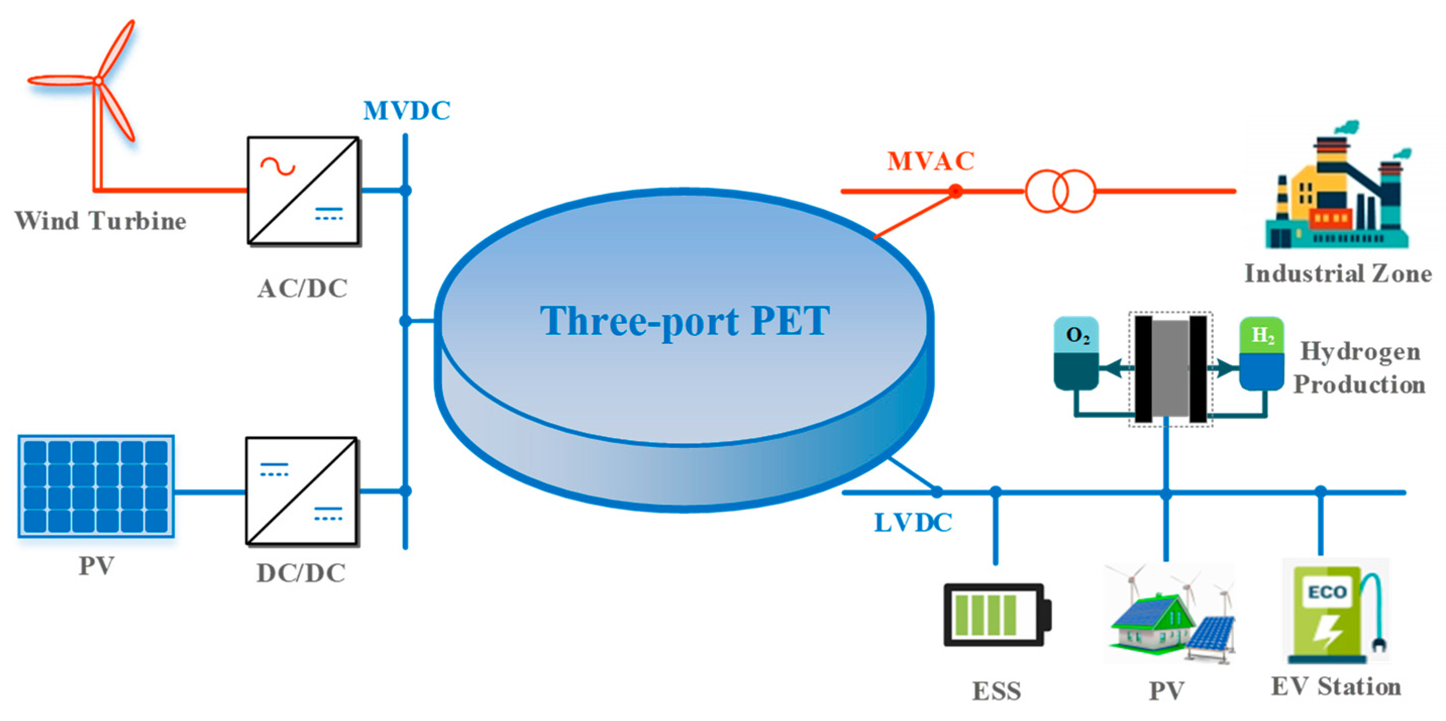
Therefore, an MMC-based three-port PET based on magnetic integration is proposed in this paper. As shown in Figure 1, by using the proposed three-port PET, the MVDC and LVDC grids can be interconnected with the traditional medium-voltage AC (MVAC) grid. Then with the flexible power control ability of the proposed three-port PET, the MVDC, MVAC and LVDC grids are able to support each other, particularly for the case of grids with high penetration of renewable energy, and DC loads. The proposed PET enables a compact design that reduces the number of magnetic components and power cells. It is especially suitable for the applications which require 100s of kW of power tapped from an LVDC port.
2. Description of the Proposed PET Topology
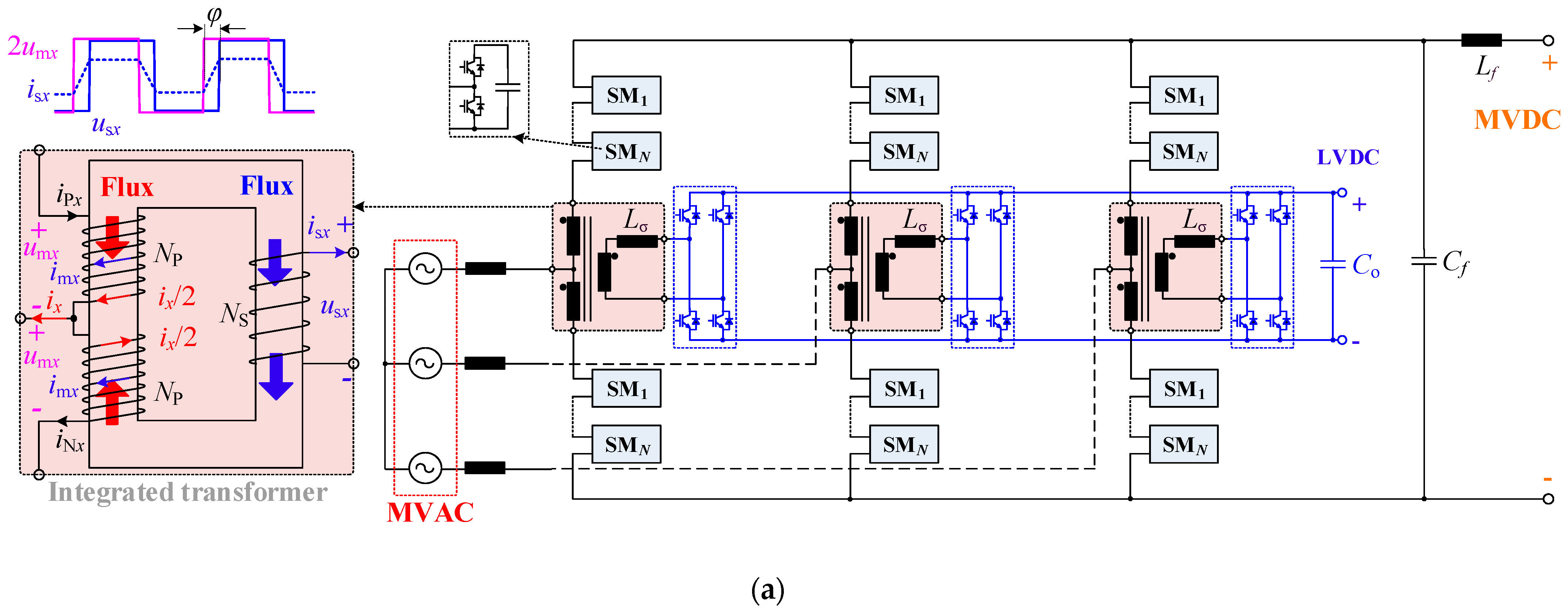
The schematic of the proposed PET is depicted in Figure 2a. Based on a typical MMC, in each phase, the arm inductors are incorporated into the same core of HF transformer to form an integrated transformer. The integrated transformer consists of a primary winding with center tap and a secondary winding. The primary winding also acts as arm inductors and its center tap is connected to the MVAC port by the transformer leakage inductance Lg. Meanwhile, the secondary winding is connected to LVDC port through leakage inductance Lσ and an H-bridge. In addition, an MMC DC bus is connected to the MVDC port via a small LC filter. In this structure, six arm inductors and a large number of transformers in traditional MMC-based PET [7] are simplified to three integrated transformers, which reduces the core material [14]. Moreover, an LVDC port can be obtained on the secondary side with only three H-bridges. Thus, the proposed PET enables a compact design that reduces the number of magnetic components and power cells (its economic benefits have been demonstrated in Section 6).
The basic principle of the proposed PET is to control MVDC, MVAC, and LVDC ports, respectively, by using DC, low-frequency (LF), and HF components of MMC. Then the upper and lower arm voltages uPx and uNx, and the upper and lower arm currents iPx and iNx of “x” phase (x = a, b, c) are
where ½uMVDC, ux and umx are the DC, LF, and HF voltage components, respectively, ⅓iMVDC, ½ix and imx are DC, LF and HF current components, respectively. Note that the HF voltage umx is applied on the primary windings of the integrated transformer, and there is another HF voltage usx generated by the H-bridge on secondary side. By adjusting the phase shift angle φ between umx and usx, the LVDC port power can be controlled (similarly to DAB).
The DC, LF and HF current components all flow through the primary winding of the integrated transformer and they are separable, which is the basis for achieving three ports. For the DC component, it flows through the primary winding and enters the MVDC port with no effects on MVAC and LVDC ports. For LF current component, it never enters the MVDC port but flows into the MVAC port via the center tap, where the currents split in the primary winding and have an inverse direction. Thus, the magnetic fluxes (marked as red in Figure 2a) excited by LF currents are cancelled, without affecting the secondary LVDC port. For the HF current component, it has the same direction in the split primary windings thus obtaining a mutually intensified magnetic flux (marked as blue in Figure 2a), which transfers power to the secondary side LVDC port. Note that HF current also flows through the primary winding and enters the MVDC bus. Fortunately, a small filter capacitor Cf can provide low-impedance return path for the HF current. To sum up, the three current components correspond to the three-port power transfer, respectively.
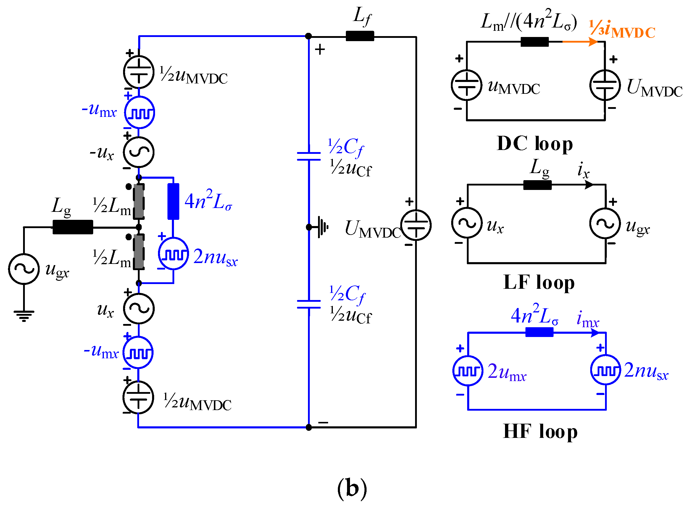
According to the DC, LF and HF components, the three port equivalent circuit loops, namely DC loop, LF loop and HF loop can be extracted, individually, as shown in Figure 2b.
DC loop: since the filter capacitor Cf provides a low-impedance for HF voltages, umx does not influence the MVDC voltages and hence is ignored for simplicity. LF voltages in upper and lower have opposite polarity so they are eliminated in DC loop. Finally, the DC loop dynamics can be expressed as
where UMVDC is MVDC port voltage.
LF loop: voltage equations of the upper and lower arms are
Subtracting (4) from (3), the DC and HF components in the upper and lower arms are eliminated, thus we have
HF loop: for the HF voltages, inductance Lm and Lf can be approximated as open circuit, and Cf represented by a short circuit. Then expression of the HF loop can be obtained as
In summary, it can be seen from (2), (5) and (6), the current of the MVDC, MVAC and LVDC ports can be independently controlled by adjusting the DC uMVDC, LF ux, and HF umx components of the arm voltage, respectively.
3. Key Parameters Design
3.1. Turn Ratio of Integrated Transformer
The turns ratio n = NP:NS (NP and NS are the turns of primary and secondary windings) is considered for matching HF voltage amplitude Um and LVDC voltage ULVDC, thus it can be designed as n = Um:ULVDC. To avoid over-modulation of the arm voltage, we have
where UMVAC is the amplitude of MVAC voltage.
3.2. Leakage Inductance of Integrated Transformer
To meet the LVDC power transfer requirement, the leakage inductance Lσ can be determined by
where φmax is the phase shift angle at maximum LVDC power PLVDC_max, and fm is the frequency of HF voltage.
3.3. Magnetizing Inductance of Integrated Transformer
The magnetizing inductance Lm limits the HF current ripple. The maximum HF current ripple (peak to peak) on magnetizing inductance is
then Lm can be calculated by (9) under a given allowable maximum HF current ripple.
3.4. Winding Arrangement
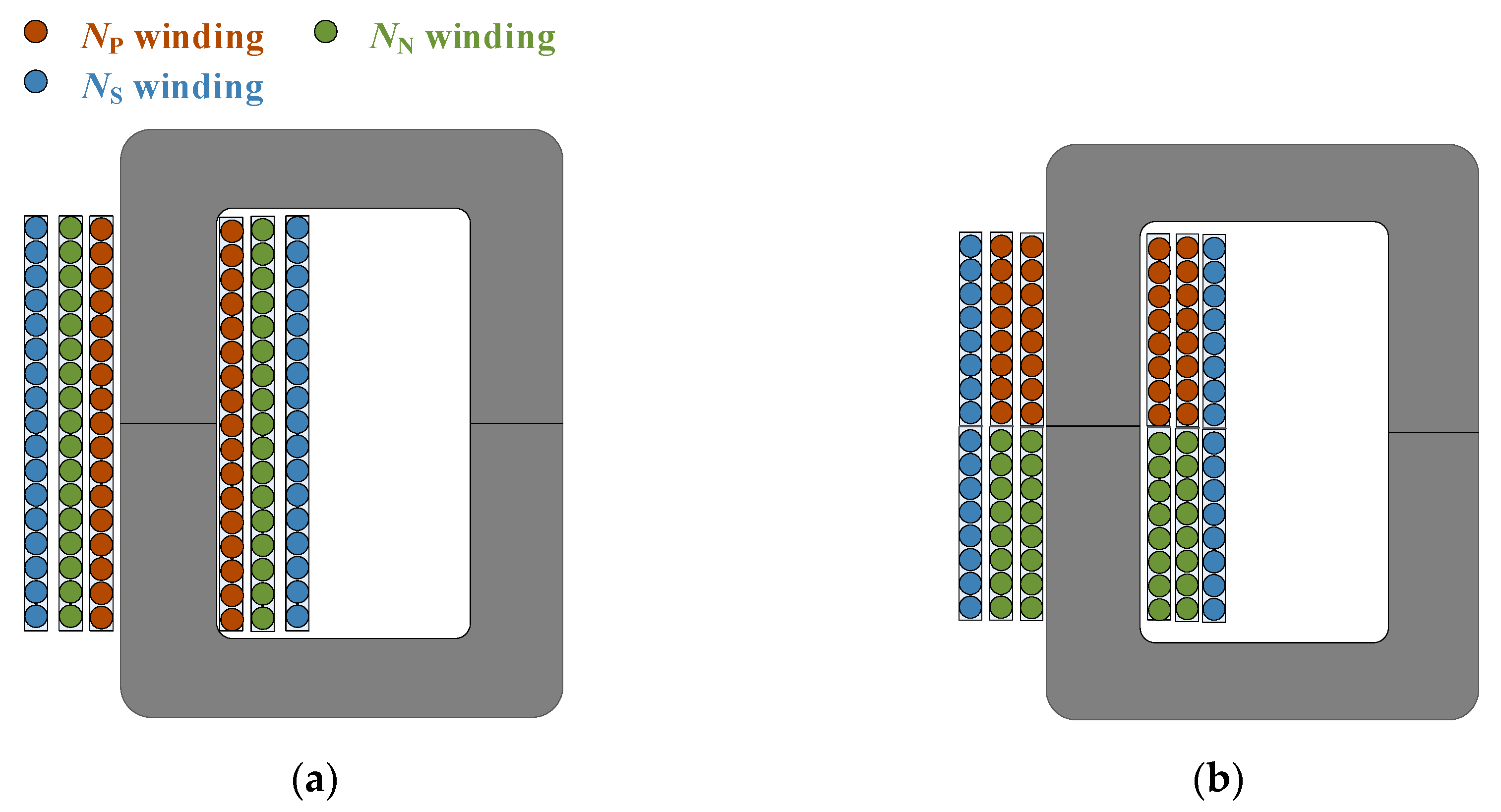
To ensure both the NP and NN windings have equal inductance, firstly, turns number NP and NN should be designed as a same value. Secondly, a proper winding arrangement is needed to ensure NP and NN windings have a same distance between NS winding, which makes their leakage inductance equal. Two typical winding arrangements in the U-core are shown in Figure 3; when the layered structure in Figure 3a is selected, leakage inductance of NP and NN windings are not equal due to the different distances between the windings. In contrast, the stacked structure in Figure 3b is recommended in this paper, which limits the deviations in the leakage inductance. Finally, with the above winding arrangement, the same inductance in the NP and NN windings can be ensured in theoretical analysis.
3.5. MVDC Filter
At the MVDC port, a small filtering capacitor Cf is installed to provide low-impedance return path for the HF currents, while a filter inductance Lf is used to block the HF current. The impedance of Cf should be far below than that of the Lf, so that Cf and Lf can be obtained by
3.6. SM Capacitors
For simplicity, the first harmonic approximation method is used to obtain SM capacitor current, which can be expressed as
where IMVDC, IMVAC, and Im are the amplitude of DC, LF and HF currents, respectively. ω and ωm are the angular frequency, φ and φm are the phase angles of the LF and HF currents, respectively. The capacitor voltage ripple (amplitude) can be obtained by integrating its current and neglecting the HF components (negligibly small), which is
where δ is phase angle of fundamental voltage ripple. The maximum voltage ripple (amplitude) can be obtained from (12) by adding the amplitudes of ω and 2ω components. Finally, the SM capacitor CSM can be calculated under a given allowable maximum voltage ripple.
4. Control Implementation
4.1. Multi-Port Control Strategy
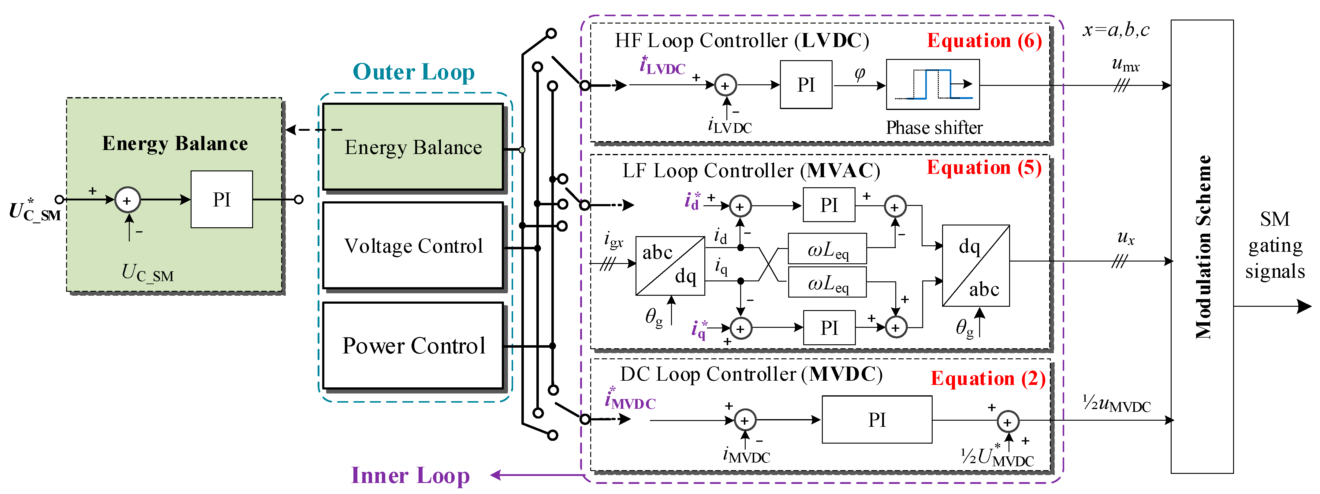
As shown in Figure 4, the proposed control strategy for the three-port PET includes an outer loop, inner loop, and modulation. The outer loop is used to calculate each port reference current, according to the requirements of voltage control, power control or PET energy balance of the SM capacitors. Based on these reference currents, the inner loop implements the current control for each port. For the MVDC port, according to (2), one PI controller is used to adjust the DC component uMVDC of arm voltage; for MVAC port, according to (5), current control based on the dq frame is used to adjust LF component ux; for LVDC port, according to (6), a PI controller is used to adjust the phase shift angle φ of HF component. As a result, the independent current control of the three ports is realized. Finally, the generated voltage components are sent to the modulation scheme.
Note that the average SM capacitor voltage is used for implementing energy balance. As shown in the “Energy Balance” diagram in Figure 4, the error between reference (U*C_SM) and sampled voltage (UC_SM) of the SM capacitors is sent to a PI controller, which adjusts the reference current of one port to absorb or release more power. Hence, the PET energy balance can be achieved by controlling the average voltage of SM capacitors to its rated value.
4.2. Modulation Scheme
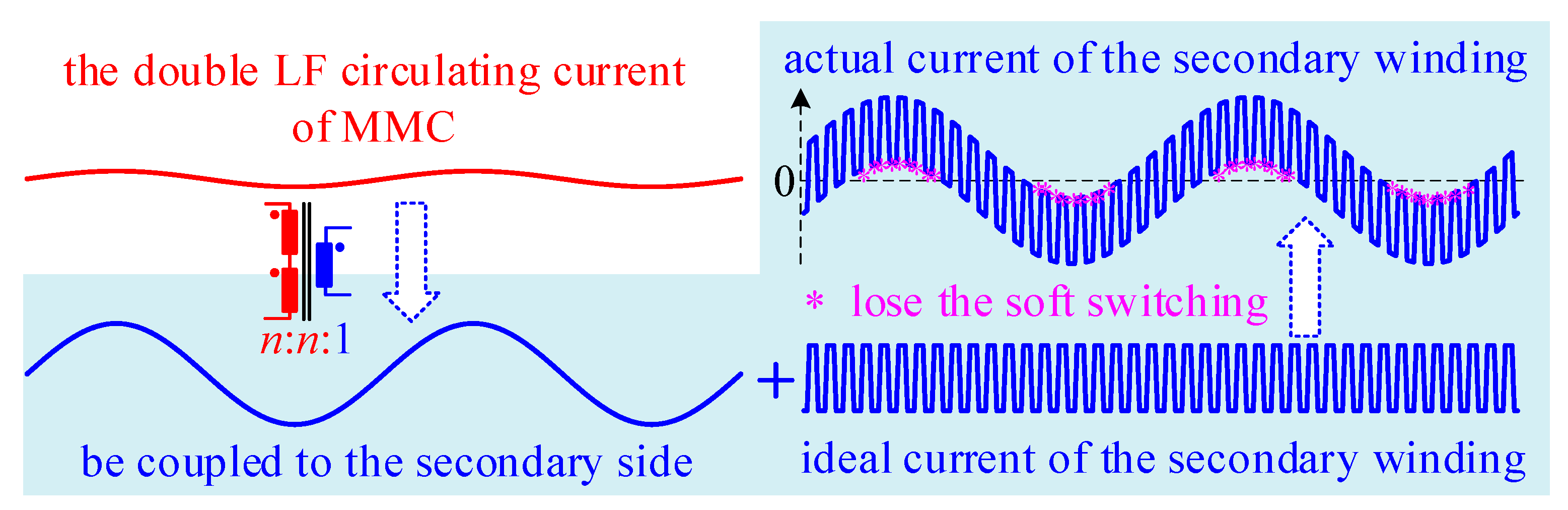
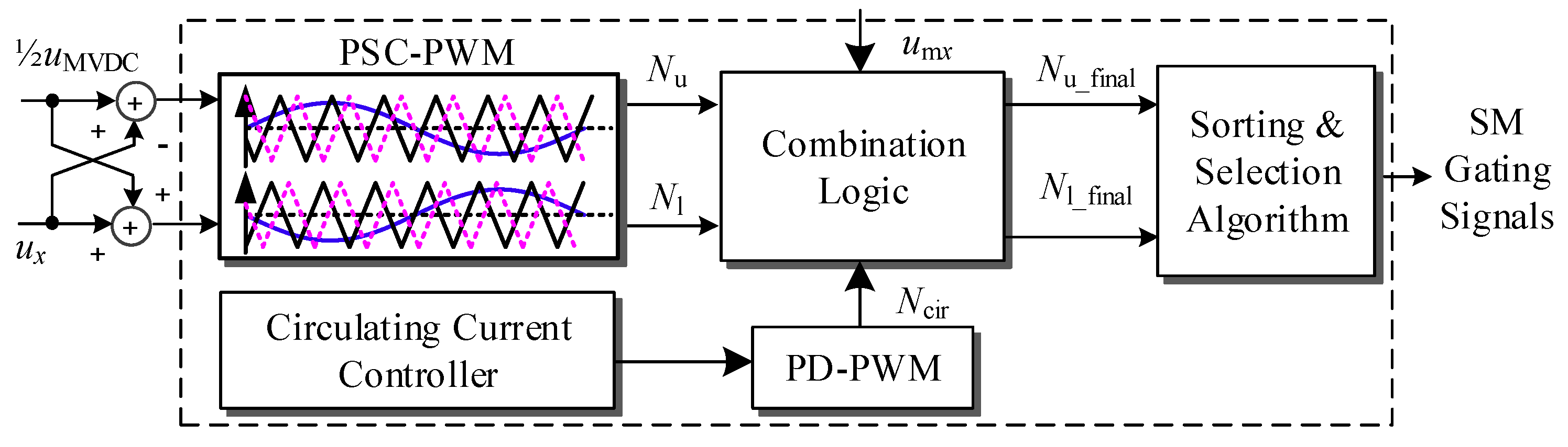
Figure 5 further considers the effects of MMC circulating current. If not well controlled, a double LF circulating current with around 1/4 amplitude of MVAC current exists [15], which is divided into magnetizing inductance and leakage inductance components (see Figure 2b). Note that the leakage inductance component reflected to secondary winding is the circulating current multiplied by 2nLm/(Lm + 4n2Lσ). It will lead to increased current stress and may lose the soft switching characteristic of the LVDC H-bridge. Thus, the decoupled modulation scheme [16] is further extended for the proposed three-port PET, as shown in Figure 6. It implements independent modulation for the DC as well as LF components, and HF as well as circulating current suppression components, respectively. Then all the modulation results are combined by combination logic, and the final number of SMs to be inserted in each arm are obtained. Finally, the gating signals of the SMs are generated after by sorting and selection algorithm.
5. Simulation and Experiment Verification
5.1. Simulation Verification
To verify the effectiveness of the proposed PET, a three-port PET with 4 MW/24 kV MVDC port, 3.5 MW/10 kVrms MVAC port and 0.5 MW/750 V LVDC port was simulated in MATLAB/Simulink. Here, one port implements constant power control, while another port dynamically adjusts power and the third port performs PET energy balance control. Each arm of the MMC contains 30 SMs, and the HF voltage is 2.4 kV/2 kHz. Detailed parameters are listed in Table 1.
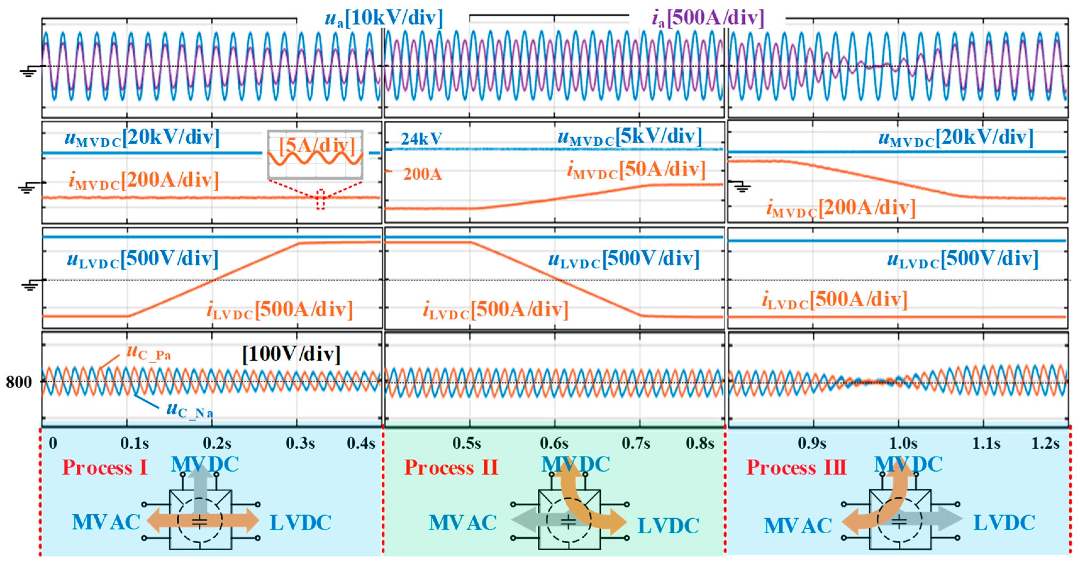
Figure 7 demonstrates the flexible power coordination of the proposed PET under three dynamic processes. In process I, the MVDC port maintains constant power (−3 MW, a negative sign indicates that power flow out from PET and a positive sign indicates flows in), which is not affected when the power between MVAC and LVDC ports changes from −0.5 MW to +0.5 MW. Then, in process II, when the coordinated power between MVDC and LVDC ports varies from 0.5 MW to −0.5 MW, the MVAC port can also keep constant power (−3.5 MW). Process III further shows that power of the LVDC port is not affected when power between the MVAC and MVDC ports are changed from −3 MW to 3.5 MW. During all these dynamic processes, the average SM capacitor voltage is kept at nominal value 800 V, indicating that PET energy is balanced. These dynamic simulation results confirmed the flexible and independent power control among three ports. From the current waveforms in Figure 7, it can be seen that HF ripple of the MVDC current is negligibly small (amplitude of 2.5A) comparing with nominal MVDC current of 167A. Additionally, the MVAC current shows that it is not affected by HF components. It can be found that the currents of three ports are continuous and smooth.
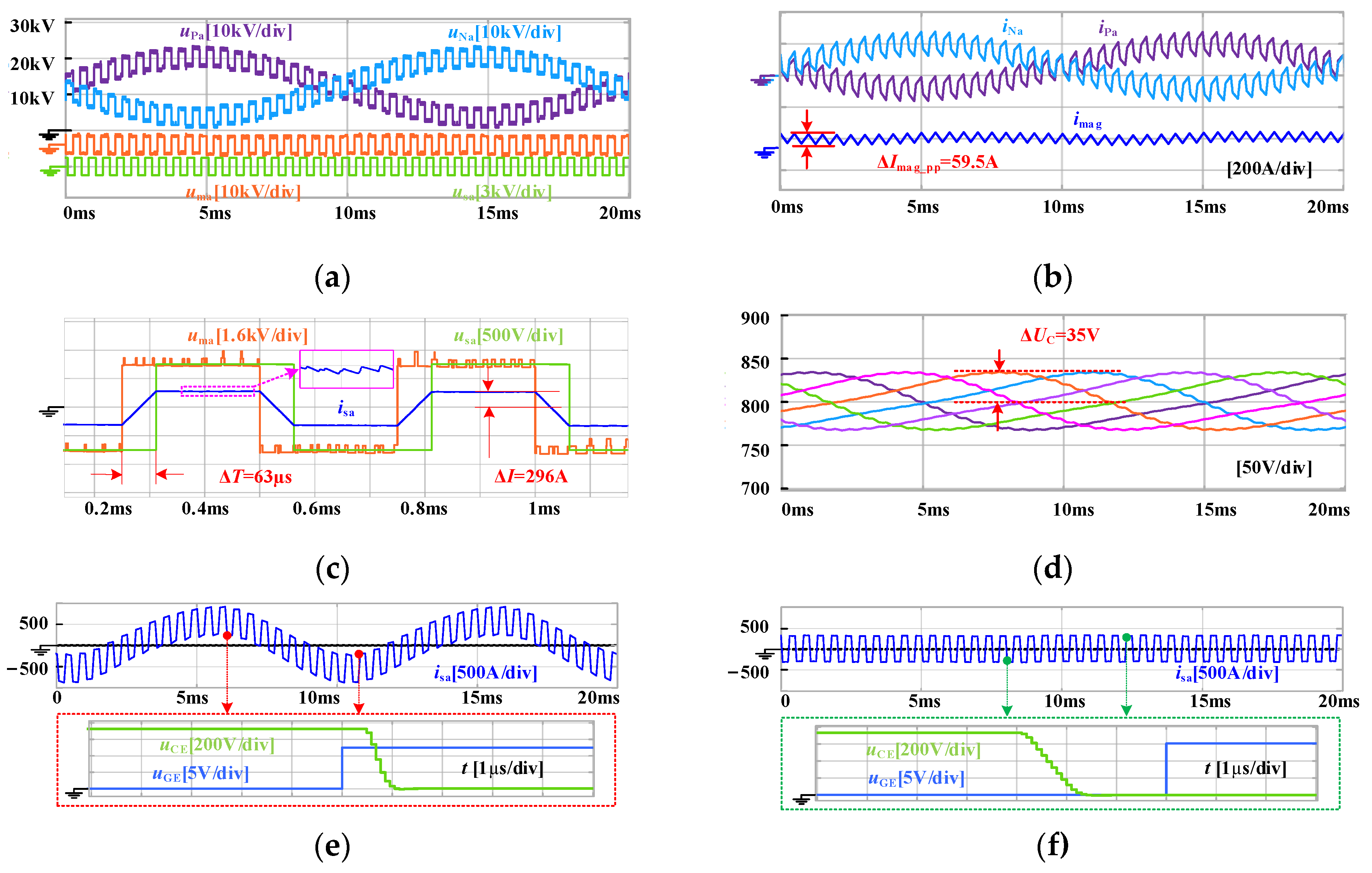
Figure 8 present the steady-state waveforms with a 4 MW MVDC port, −3.5 MW MVAC port, and −0.5 MW LVDC port, respectively. Figure 8a verifies that the arm voltage described in (1) contains 12 kV DC, 8.16 kV/50 Hz LF, and 2.4 kV/2 kHz HF voltage components. The HF voltage component is applied on the primary winding, with each split winding uma (2.4 kV/2 kHz), which is reflected to secondary winding as usa (750 V/2 kHz). The upper- and lower-arm currents are shown in Figure 8b, which contain the 56A DC, 143A/50 Hz LF, and 76A/2 kHz HF current components. The HF current ripple on magnetizing inductance ΔImag_pp = 59.5A coincides with the analyzed value in (9). Figure 8c displays a delay time ΔT = 63 µs (phase shift angle of π/4) between primary and secondary winding voltages, and secondary winding current with an amplitude of ΔI = 296A when the LVDC port power is −0.5 MW. Figure 8d shows that the SM capacitor voltage fluctuation ΔUC = 35 V keeps well below the maximum allowable value as calculated in (12). As shown in Figure 8e, if the circulating current is not well controlled, the secondary HF current is superimposed with a double LF fluctuation, resulting in current stress up to 900A. It also distorts the secondary winding current so that the IGBT junction capacitance cannot be discharged before it turns on (collector-emitter voltage uCE remains high when switching on the moment uGE is activated). This means the zero-voltage switching characteristic of the LVDC H-bridge is lost. After incorporating the proposed modulation scheme, the double LF fluctuation has been eliminated, as shown in Figure 8f, and the current stress is reduced to 296A while the zero-voltage switching is ensured.
5.2. Experiment Verification
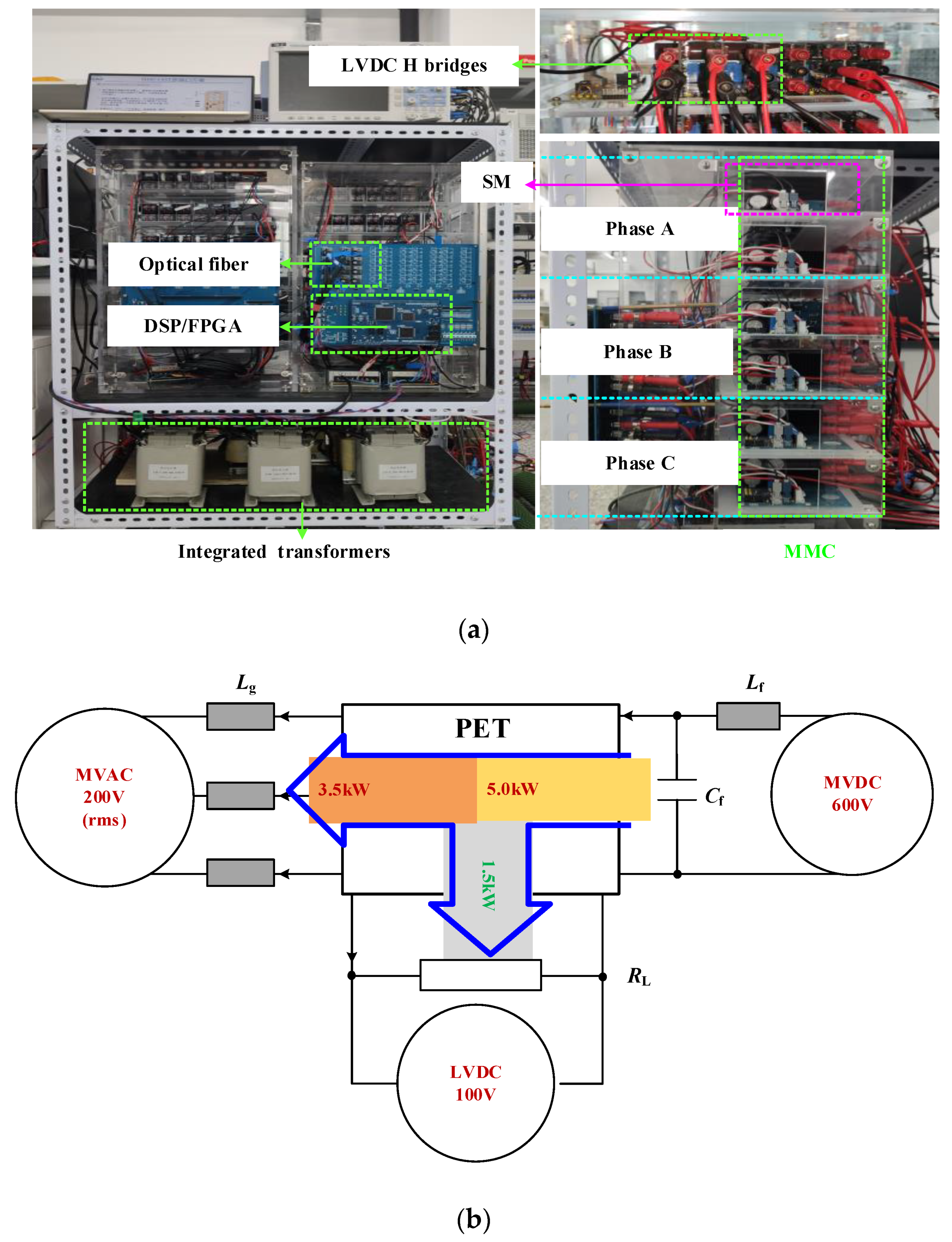
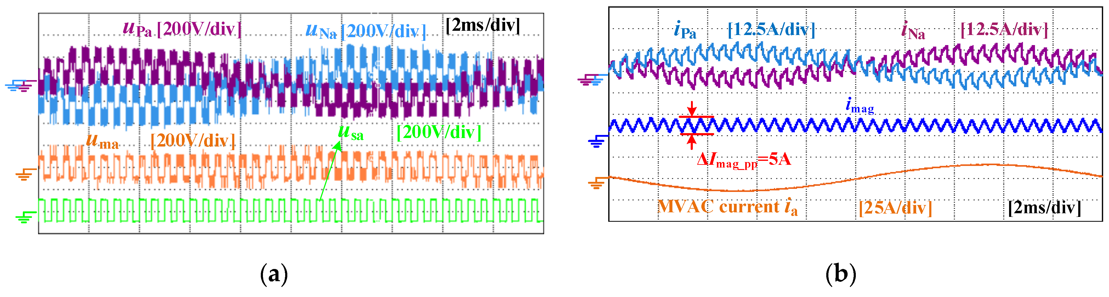
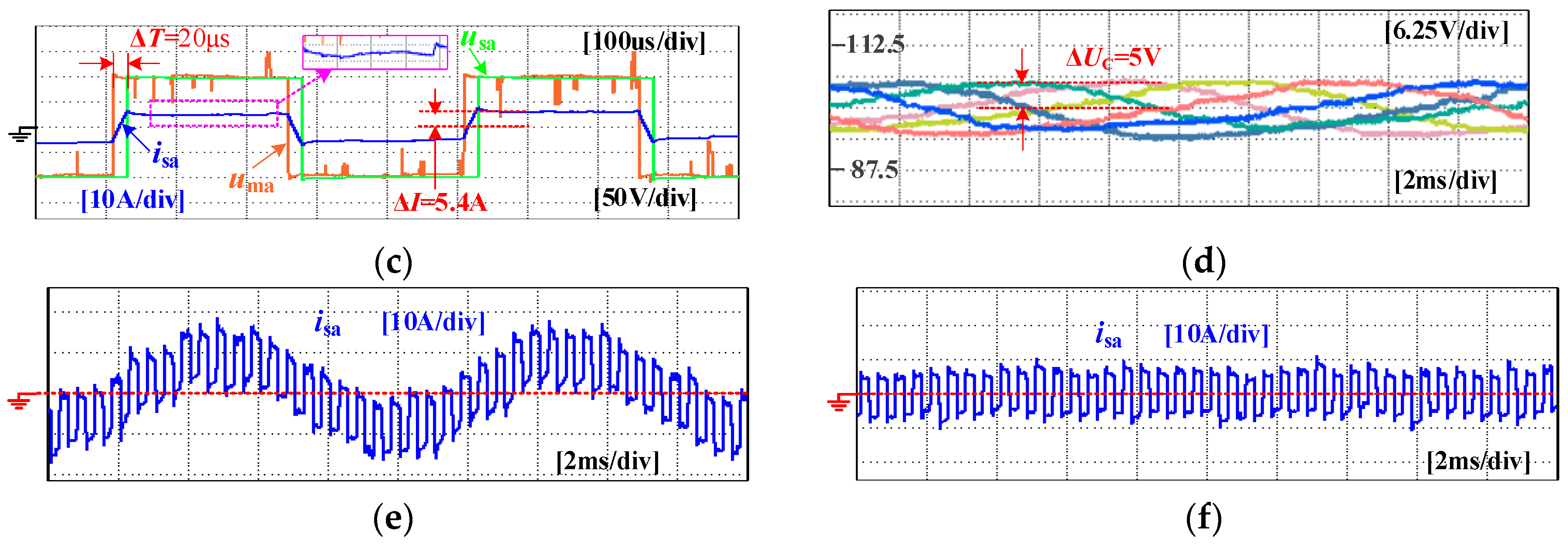
To further verify the proposed PET, a downscaled prototype with six SMs per arm, has been built as in Figure 9a. The ferrite magnetic core chosen for integrated transformers is UU66/55/40. The inner and outer loop control algorithms are implemented in the TMS320F28377D DSP, while an EP3C25Q240 FPGA is used to perform the modulation scheme. As shown in Figure 9b, the prototype was tested at the condition of 5 kW/600 V MVDC port, 3.5 kW/200 Vrms MVAC port and 1.5 kW/100 V LVDC port. Compared with simulations, the experimental values of MVAC inductance Lg, magnetizing inductance Lm, MVDC inductance Lf and SM capacitors are smaller due to downscaled voltages and currents. The leakage inductance is larger because the LVDC power is only 1.5 kW. In addition, since there are only six SMs in each arm, the SM switching frequency is higher (6 kHz) in experiments. Detailed experiment parameters are listed in Table 1. Experimental results in Figure 10a verifies that the arm voltage contains 300 V DC, 163 V/50 Hz LF and 100 V/2 kHz HF components. The HF voltages applied on primary (uma) and secondary (usa) winding can be observed as 100 V/2 kHz. Similarly, Figure 10b shows that the upper- and lower-arm currents contain 2.8A DC, 7.1A/50 Hz LF, and 5.2A/2 kHz HF components. The HF current ripple on magnetizing inductance ΔImag_pp = 5A also agrees with the analyzed value as calculated in (9). The MVAC current waveform confirms that it has not been affected by HF components. Figure 10c shows a phase shift angle of π/12 (ΔT = 20 µs) between primary and secondary winding voltages, and the secondary winding current amplitude is ΔI = 5.4 A, when LVDC power is 1.5 kW. It can be found in Figure 10d that the SM capacitor voltage fluctuation ΔUC = 5 V keeps well below the maximum allowable value as calculated in (12). After applying the proposed modulation scheme, the current stress of 18A [see Figure 10e] is reduced to below 10A [see Figure 10f], and the soft switching characteristic is guaranteed as the double LF fluctuation has been eliminated. As shown in Figure 8 and Figure 10, there are some differences in values between experiments and simulations. However, the experiment matches the simulation well in principle. In fact, there are some switching spikes (at MMC equivalent switching frequency of fSW = n × fS) existing in the HF current waveform isa, which are caused by switching of MMC SMs. As shown in Figure 8c and Figure 10c, the switching spikes are negligibly small because the leakage inductance Lσ has a high impedance for switching frequency (30 kHz and 36 kHz for simulation and experiment, respectively), and these detailed switching spikes can be found in the zoom-in waveform of isa.
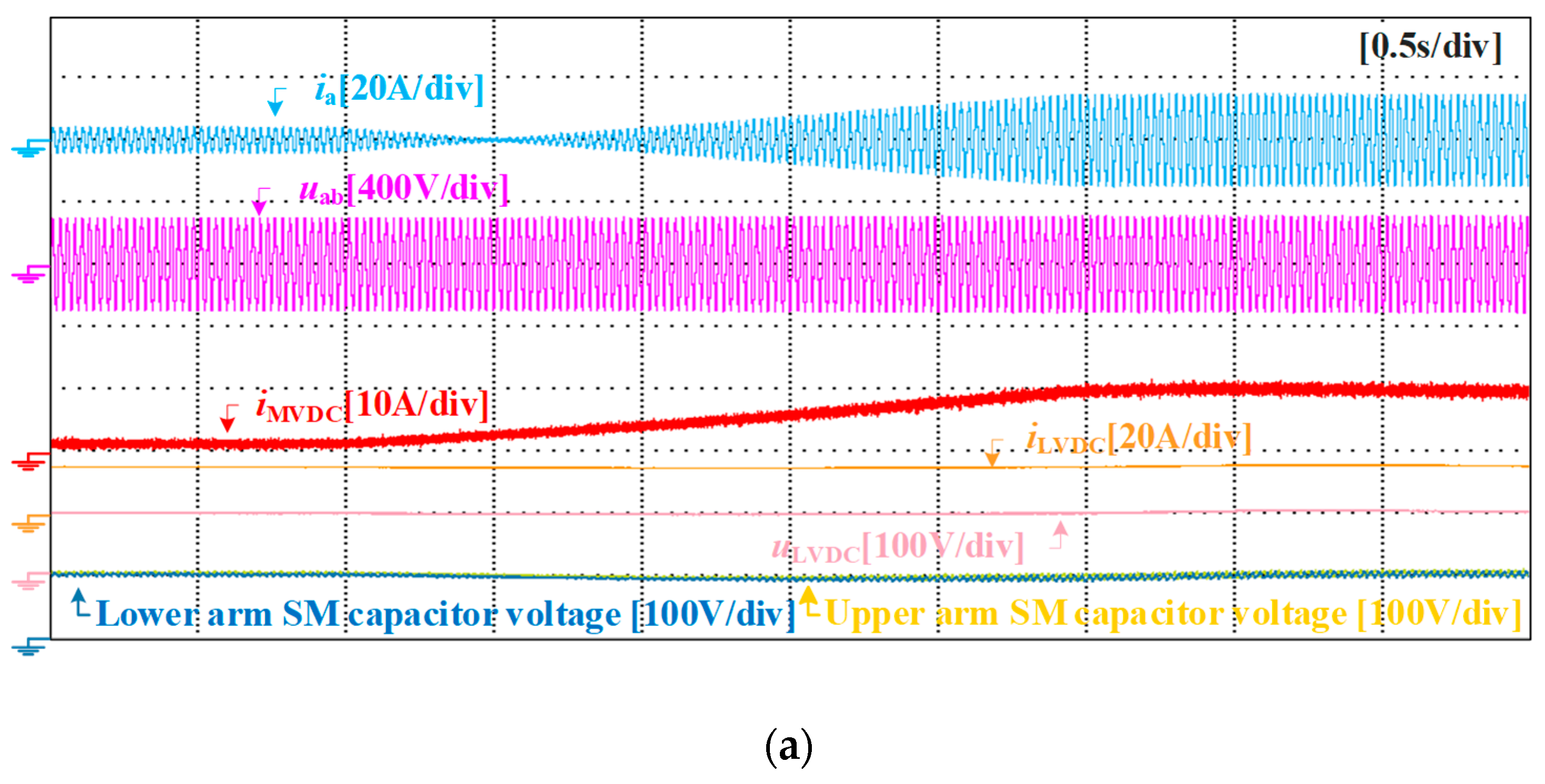
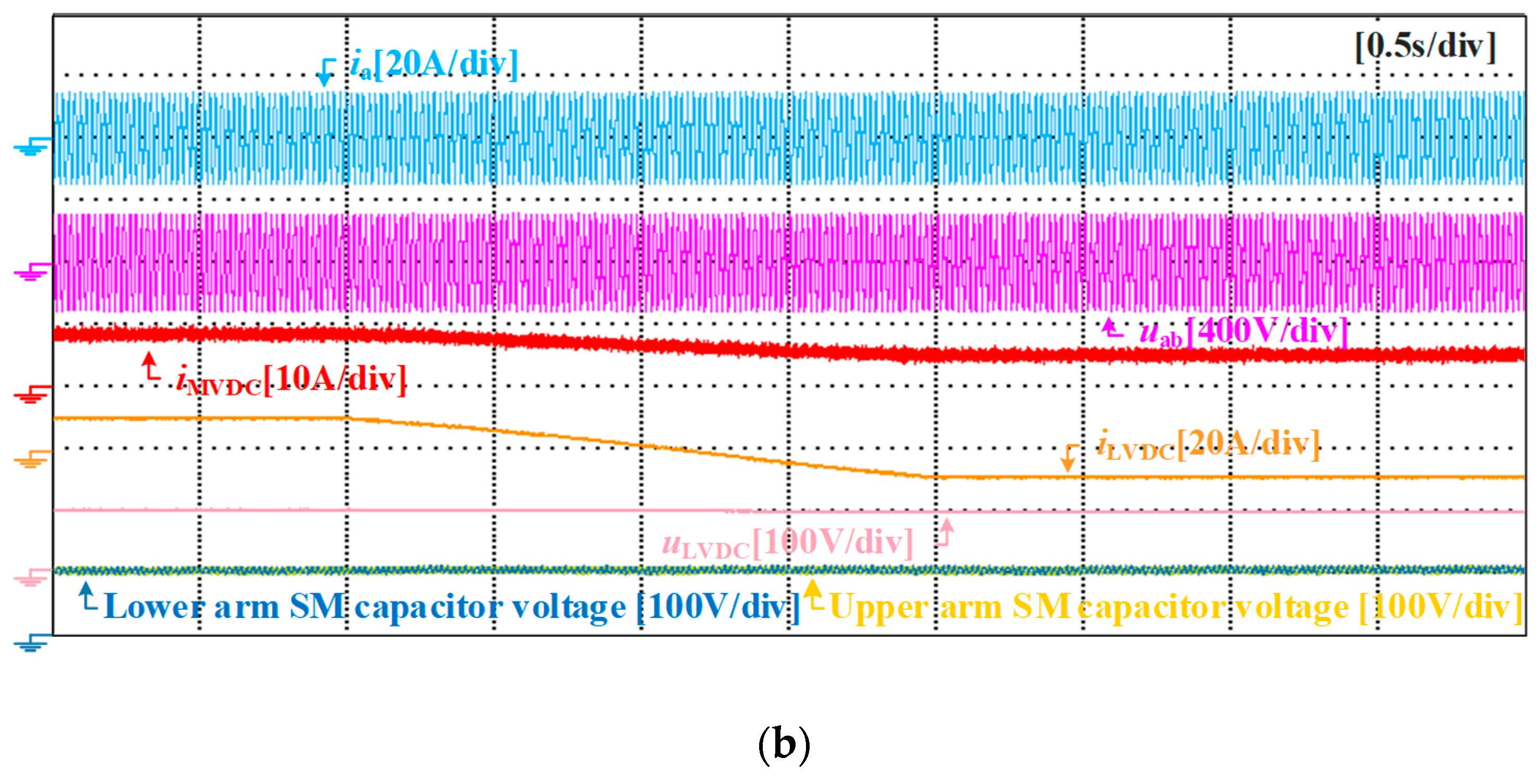
Figure 11 further provides the experimental verifications under dynamic power exchange condition to illustrate the stability. The MVAC/MVDC ports dynamic power exchange results are shown in Figure 11a, while the LVDC/MVDC ports dynamic power exchange results are shown in Figure 11b. In Figure 11a, LVDC port implements constant power control, while MVAC port dynamically adjusts power and the MVDC port performs PET energy balance control. During 1.0 s~8.5 s, the power between MVAC and MVDC ports changes from −1 kW to +3.5 kW, the LVDC port maintains constant power of 1.5 kW, the voltages and currents of all ports are smooth. During these dynamic processes, the SM capacitor voltage is kept at nominal value 100 V, indicating that PET energy is balanced. Figure 11b further shows the operation waveforms when the power between LVDC and MVDC ports changes from −1 kW to +1 kW, it can be also found that the voltages and currents of all ports are smooth, and the SM capacitor voltage is kept at nominal value as well.
6. Economic Benefits Analysis
In this section, the economic benefits of the proposed PET have been demonstrated by comparing it with existing typical multi-port PETs in [4,7], which distributionally add DABs to each MMC SM capacitor (MMC + distributed DABs). The comparison contains the magnetic volume and the device cost, where the simulation condition of 4 MW/24 kV MVDC port, 3.5 MW/10 kVrms MVAC port and 0.5 MW/750 V LVDC port is selected for case study.
6.1. Magnetic Volume Comparison
For magnetic volume comparison shown in Table 2, the arm inductors and transformers volume are the main considerations. The parameters of integrated transformer of the proposed PET are selected as same as simulation value in Table 1, where the turn ratio n = 3.2, magnetizing inductance Lm = 20 mH, and leakage inductance Lσ = 158.2 µH. The total arm inductors (Larm = 2.4 mH) of the MMC + distributed DABs PET is equal to the equivalent arm inductors of the proposed PET, which is formed by magnetizing inductance and leakage inductance in parallel [2 Larm = (4n2 Lσ × Lm)/(4n2 Lσ + Lm)].
The volume of transformer or inductor can be obtained from their area product AP, calculating by Vmagn = Kvol (AP)0.75 [17]. The area product of a transformer is proportional to the total apparent power of all windings, while the area product of inductor (L) is proportional to the maximum energy storage W = ½LI2peak, where Ipeak is the peak value of inductor current. Thus, the area product of the transformer with K (K ≥ 2) windings can be obtained by (13) [14], and the area product of inductor can be expressed as (14) [17].
where Pj is the processed power of jth winding, Kf is the waveform factor, KW is the core window utilization factor, Jrms is the rms current density of the winding, Bmax is the maximum magnetic flux density, and f is the working frequency of transformer. Kvol is the core structure factor, which reflects the relationship between volume and area product, and it can be obtained from datasheet of magnetic core manufacturer.
For the MMC + distributed DABs PET, 6N transformers are used and each one process a total power of [2PLVDC/(6 N)]. So, the total volume of 6 N transformers can be calculated by
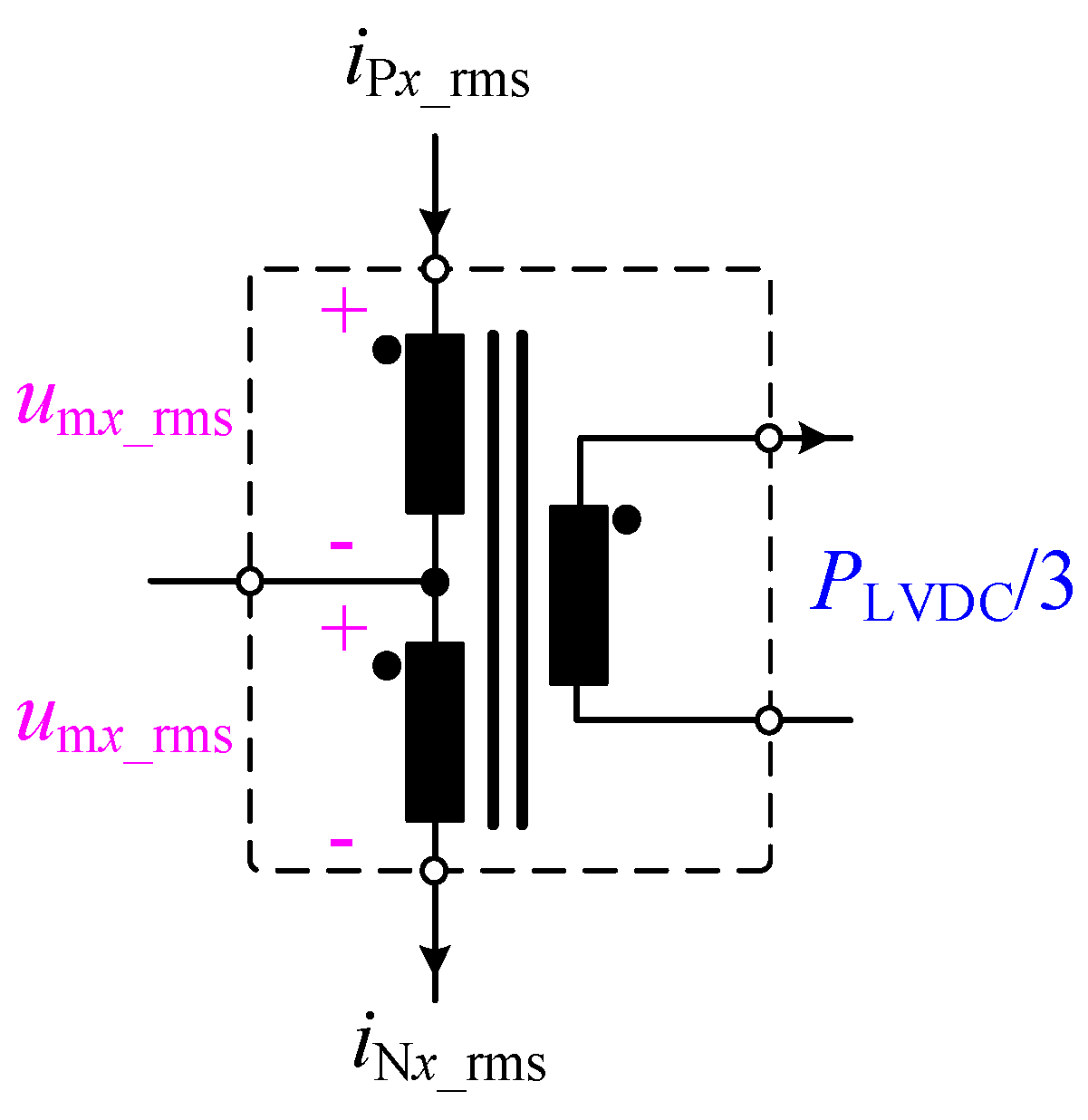
In contrast, for the proposed PET, there are only three integrated transformers. In each transformer, as shown in Figure 12, each split primary winding process a power of (umx_rmsiPx_rms), while the secondary winding power is PLVDC/3, thus the total power of all windings of the integrated transformer is (2umx_rmsiPx_rms + PLVDC/3). Then the total volume of the three integrated transformers can be calculated by
where umx_rms and iPx_rms is the rms value of each primary split wingding. umx_rms is equal to the amplitude of HF voltage Um = 2.4 kV. iPx_rms can be calculated by iPx_rms = [(⅓iMVDC)2 + (½ix_rms)2 + (imx_rms)2]½, where ⅓iMVDC, ½ix_rms and imx_rms are the rms value of DC, LF and HF components of arm current, respectively. Note that, ⅓iMVDC = 56 A, ½ix_rms = 101 A and imx_rms = 70 A can be obtained according to three-port power condition. It can be found from (15) that, the total transformer volume of MMC + distributed DABs PET is positively related to the number of transformers 6N. In this study case with n = 30, which is meeting medium voltage applications, it can be found that transformers volume of the proposed PET (1.02 m3) is much smaller than that of MMC + distributed DABs PET (1.46 m3).
Furthermore, the proposed PET saved six arm inductors which are needed in MMC + distributed DABs PET. According to (14), these six arm inductors volume can be calculated as
where ½IMVAC = 143 A is peak value of LF current, which can be obtained according to MVAC port power condition. Then, total arm inductors volume can be calculated as 1.94 m3.
Finally, six arm inductors and 6N transformers in MMC + distributed DABs PET have a total magnetic volume of 3.40 m3. Since these transformers and arm inductors are simplified into three integrated transformers in the proposed PET, it has a lowest magnetic volume (1.02 m3). The magnetic volume of the other two existing typical PETs (CHB + common HF bus PET and MMC + ISOP DABs PET) can be obtained by the same way discussed above, and the results are also shown in Table 2. It can be found that the proposed PET saves more than 60% of magnetic volume compared with the existing typical PET.
6.2. Device Cost Comparison
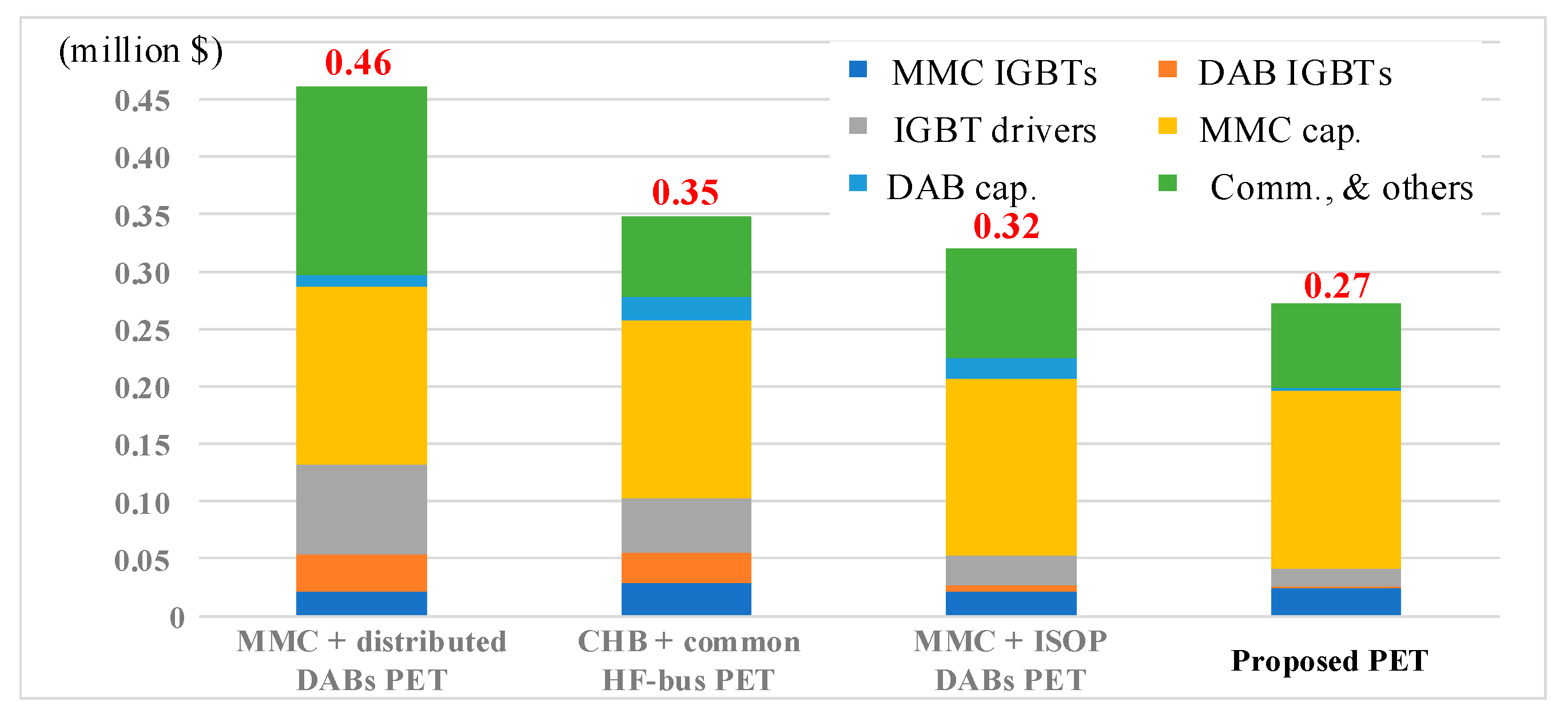
The submodule device cost comparison of proposed PET with MMC + distributed DABs PET was shown in Table 3 and Figure 13. It mainly contains the cost of IGBTs, IGBT drivers, capacitors, and other auxiliary components (including fiber communication, auxiliary power supply, sampling, voltage transducer, controller ICs and copper busbar).
For the cost of IGBTs, all the MMC and DAB IGBTs are selected from Infineon Technology according to device current stress. Since the MMC current stress of the proposed PET (275A) is slightly larger than that of the MMC + distributed DABs PET (199A), it leads to higher MMC IGBT cost (an increase of $4140). However, the cost of DAB IGBTs in the proposed PET (only six half-bridge modules are needed) is much lower (a reduction of $32,310) than that of MMC + distributed DABs PET (720 half-bridge modules). Finally, the total IGBTs cost of proposed PET results in a saving of $28,170 compare to MMC + distributed DABs PET.
For the cost of IGBT drivers, it is directly proportional to the number of IGBTs, thus the total cost of IGBT drivers of MMC + distributed DABs PET ($78,300) is significantly higher than proposed PET ($16,182).
For the cost of capacitors, all the SMs capacitors in each PET are the same (5.5 mF), thus the cost of MMC capacitors is equal ($154,800). Although the total capacity of DAB capacitors is the same (under the same voltage ripple of 2%), the cost of DAB capacitors of MMC + distributed DABs PET ($9900) is higher than that of the proposed PET ($1932), since too many capacitors need to be installed. So, the total cost of capacitors in the proposed PET results in a saving of about $7968 compared to the MMC + distributed DABs PET.
For the cost of auxiliary components, due to the considerable number of DABs (6N) in the MMC + distributed DABs PET, there are too many extra fiber communication, auxiliary power supply, A/D sampling, voltage transducer, controller ICs and copper busbar used for the DABs, which significantly increases the cost of PET. Thus, as shown in Table 3 and Figure 13, the total cost of auxiliary components in the MMC + distributed DABs PET ($0.16 million) is much higher than the proposed PET ($0.07 million).
In summary, although a slightly higher MMC IGBTs cost in proposed PET, there is a significant reduction in cost in DAB IGBTs, IGBT drivers and auxiliary components, in comparison with the MMC + distributed DABs PET. The device cost of the other two existing typical PETs (CHB + common HF bus PET and MMC + ISOP DABs PET) can be obtained by the same manner discussed above, and all the results are shown in Figure 13. It can be found that the proposed PET has a minimum device cost (total cost of $0.27 million) compared with the CHB + common HF bus PET (total cost of $0.35 million), MMC + distributed DABs PET (total cost of $0.46 million) and MMC + ISOP DABs PET (total cost of $0.32 million). It can be concluded that the proposed PET saves more than 19% of the device cost compared with the existing typical PETs. Furthermore, although the cost of magnetic components is unavailable here, it can be predicted that the total costs of magnetic components in the proposed PET will be lower, according to listed magnetic volume in Table 2.
7. Conclusions
A three-port PET based on magnetic integration is proposed in this paper. By applying an integrated transformer where the primary winging is used to form the MMC arm inductors and the LVDC port can be obtained on secondary side, a compact three-port PET can be realized which reduces the magnetic volume and the number of SMs. It is clear that the reduced number of SMs leads to a cost benefit due to the reduction in insulation, enclosures, and auxiliary circuits. The proposed topology is especially suitable for the applications where moderate amounts of power (100s of kW) are tapped from an LVDC port.
Author Contributions
Conceptualization, B.L.; methodology, Z.L.; software, Z.S.; validation, L.H.; formal analysis, X.Z.; writing—original draft preparation, Z.L.; writing—review and editing, Y.J.; project administration, D.X. All authors have read and agreed to the published version of the manuscript.
Funding
This research was funded by National Natural Science Foundation of China under Grants 51720105008 and 52177173.
Institutional Review Board Statement
Not applicable.
Informed Consent Statement
Not applicable.
Data Availability Statement
Not applicable.
Conflicts of Interest
The authors declare no conflict of interest.
References
- Huber, J.E.; Kolar, J.W. Applicability of solid-state transformers intoday’s and future distribution grids. IEEE Trans. Smart Grid 2019, 10, 317–326. [Google Scholar] [CrossRef]
- Gorla, N.B.Y.; Kolluri, S.; Chai, M.; Panda, S.K. A comprehensive harmonic analysis and control strategy for improved input power quality in a cascaded modular solid state transformer. IEEE Trans. Power Electron. 2019, 34, 6219–6232. [Google Scholar] [CrossRef]
- Nie, J.; Yuan, L.; Wen, W.; Duan, R.; Shi, B.; Zhao, Z. Communication independent power balance control for solid state transformer interfaced multiple power conversion systems. IEEE Trans. Power Electron. 2020, 35, 4256–4271. [Google Scholar] [CrossRef]
- Sun, X.; Teng, J.; Bu, Z.; Pan, Y.; Zhao, W.; Li, X. Research on triple-port SST scheme based on the natural elimination of MMC sub-modules voltage fluctuation and imbalance. IEEE Trans. Emerg. Sel. Topics Power Electron. 2021, 10, 3697–3710. [Google Scholar] [CrossRef]
- Wen, W.; Li, K.; Zhao, Z.; Yuan, L.; Mo, X.; Cai, W. Analysis and control of a four-port megawatt-level high-frequency-bus-based power electronic transformer. IEEE Trans. Power Electron. 2021, 36, 13080–13095. [Google Scholar] [CrossRef]
- Li, K.; Wen, W.; Zhao, Z.; Yuan, L.; Cai, W.; Mo, X.; Gao, C. Design and implementation of four-port megawatt-level high-frequency-bus based power electronic transformer. IEEE Trans. Power Electron. 2021, 36, 6429–6442. [Google Scholar] [CrossRef]
- Zhou, J.; Zhang, J.; Wang, J.; Zang, J.; Shi, G.; Feng, X.; Cai, X. Design and control of power fluctuation delivery for cell capacitance optimization in multiport modular solid-state transformers. IEEE Trans. Power Electron. 2021, 36, 1412–1427. [Google Scholar] [CrossRef]
- Li, Z.; Wang, P.; Chu, Z.; Zhu, H.; Sun, Z.; Li, Y. A three-phase 10 kVAC-750 VDC power electronic transformer for smart distribution grid. In Proceedings of the 2013 15th European Conference on Power Electronics and Applications (EPE), Lille, France, 2–6 September 2013; pp. 1–9. [Google Scholar]
- Gao, F.; Li, Z.; Wang, P.; Xu, F.; Chu, Z.; Sun, Z.; Sun, Z.; Li, Y. Prototype of smart energy router for distribution DC grid. In Proceedings of the 2015 17th European Conference on Power Electronics and Applications (EPE’15 ECCE-Europe), Geneva, Switzerland, 8–10 September 2015; pp. 1–9. [Google Scholar]
- Ma, D.; Chen, W.; Shu, L.; Qu, X.; Hou, K. A MMC-based multiport power electronic transformer with shared medium-frequency transformer. IEEE Trans. Circuits Syst. II Exp. Briefs 2021, 68, 727–731. [Google Scholar] [CrossRef]
- Ma, D.; Chen, W.; Shu, L.; Qu, X.; Zhan, X.; Liu, Z. A multiport power electronic transformer based on modular multilevel converter and mixed-frequency modulation. IEEE Trans. Circuits Syst. II Exp. Briefs 2020, 67, 1284–1288. [Google Scholar] [CrossRef]
- Zheng, G.; Chen, Y.; Kang, Y. A modular multilevel converter (MMC) based solid-state transformer (SST) topology with simplified energy conversion process and magnetic integration. IEEE Trans. Ind. Electron. 2021, 68, 7725–7735. [Google Scholar] [CrossRef]
- Zheng, G.; Chen, Y.; Kang, Y. Modeling and control of the modular multilevel converter (MMC) based solid state transformer (SST) with magnetic integration. CES Trans. Electric. Machines Syst. 2020, 4, 309–318. [Google Scholar] [CrossRef]
- Pereira, T.; Hoffmann, F.; Zhu, R.; Liserre, M. A comprehensive assessment of multiwinding transformer-based DC–DC converters. IEEE Trans. Power Electron. 2021, 36, 10020–10036. [Google Scholar] [CrossRef]
- Reddy, G.A.; Shukla, A. Circulating current optimization control of MMC. IEEE Trans. Power Electron. 2021, 68, 2798–2811. [Google Scholar] [CrossRef]
- Li, B.; Han, L.; Mao, S.; Zhou, S.; Qu, Z.; Xu, D. Decoupled modulation scheme for modular multilevel converters in medium-voltage applications. IEEE Trans. Power Electron. 2020, 35, 11430–11441. [Google Scholar] [CrossRef]
- McLyman, C.W.T. Transformer and Inductor Design Handbook, 4th ed.; CRC Press: New York, NY, USA, 2011. [Google Scholar]
Figure 1.
Application of the proposed three-port PET.

Figure 2.
The proposed three-port PET: (a) circuit topology; (b) equivalent circuit of “x” phase (the blue line indicates the HF loop).
Figure 2.
The proposed three-port PET: (a) circuit topology; (b) equivalent circuit of “x” phase (the blue line indicates the HF loop).


Figure 3.
Winding arrangement: (a) layered structure; (b) stacked structure.

Figure 4.
Multi-port control strategy (variables with * are reference values, and light green background to highlight the Energy Balance block).
Figure 4.
Multi-port control strategy (variables with * are reference values, and light green background to highlight the Energy Balance block).

Figure 5.
Effects of MMC circulating current on the LVDC side.

Figure 6.
Modulation scheme (the blue sinusoidal solid line represents the modulation signal, while the purple triangular dotted line represents the carrier).
Figure 6.
Modulation scheme (the blue sinusoidal solid line represents the modulation signal, while the purple triangular dotted line represents the carrier).

Figure 7.
Dynamic simulation results of proposed three-port PET.

Figure 8.
Steady-state simulation results: (a) arm voltages and transformer winding voltages; (b) arm currents and magnetizing current; (c) transformer winding voltages and secondary winding current; (d) six arm SM voltages; (e) secondary winding current with double LF fluctuation; (f) secondary winding HF current after applying the proposed modulation.

Figure 9.
Prototype: (a) photograph of the laboratorial three-port PET prototype; (b) circuit diagram of the test platform.
Figure 9.
Prototype: (a) photograph of the laboratorial three-port PET prototype; (b) circuit diagram of the test platform.

Figure 10.
Experiment results: (a) arm voltages and transformer winding voltages; (b) arm currents, magnetizing current and MVAC current; (c) transformer winding voltages and secondary winding current; (d) six arm SM voltages; (e) secondary winding current with double LF fluctuation; (f) secondary winding HF current after applying the proposed modulation.


Figure 11.
Dynamic experimental results: (a) power transfer between the MVAC and MVDC port; (b) power transfer between the LVDC and MVDC port.
Figure 11.
Dynamic experimental results: (a) power transfer between the MVAC and MVDC port; (b) power transfer between the LVDC and MVDC port.


Figure 12.
The processed power of each winding of integrated transformer.

Figure 13.
Devices cost comparison of proposed PET with existing typical PETs.


Table 1.
Parameters of proposed PET.
| Parameters | Simulation Value | Experiment Value |
|---|---|---|
| Line-to-line RMS voltage of MVAC | 10 kV | 200 V |
| Rated MVDC voltage | 24 kV | 600 V |
| Rated LVDC voltage | 750 V | 100 V |
| Line MVAC inductance Lg | 10 mH | 2 mH |
| Rated SM capacitor voltage USM | 800 V | 100 V |
| MMC SM capacitor CSM | 5.5 mF | 2 mF |
| Number of SM per arm n | 30 | 6 |
| Magnetizing inductance of HF transformer Lm | 20 mH | 10 mH |
| Leakage inductance of HF transformer Lσ | 158.2 µH | 368 µH |
| Switching frequency of SM fs | 1 kHz | 6 kHz |
| Frequency of injected HF voltage | 2 kHz | 2 kHz |
| HF transformer turn ratio n:n:1 | 3.2:3.2:1 | 1:1:1 |
| MVDC inductance Lf | 600 µH | 100 µH |
| MVDC capacitor Cf | 30 µF | 30 µF |
Table 2.
Magnetic volume comparison of proposed PET with existing typical PETs.
| Parameters (Kvol =17.9, Kf = 4, KW = 0.4, Jrms = 50A, Bmax = 1T, fm = 2 kHz, n = 30) | CHB + Common HF Bus PET | MMC + Distributed DABs PET | MMC + ISOP DABs PET | Proposed PET |
|---|---|---|---|---|
| Transformers volume | 10.64 m3 | 1.46 m3 | 0.93 m3 | 1.02 m3 |
| Arm inductors volume | 0.99 m3 | 1.94 m3 | 1.94 m3 | —— |
| Total magnetic volume | 11.63 m3 | 3.40 m3 | 2.87 m3 | 1.02 m3 |
Table 3.
Device cost comparison of proposed PET with existing typical PETs.
| Parameters | MMC + Distributed DABs PET | Proposed PET |
|---|---|---|
| Current stress of MMC device | (199A) | (275A) |
| Number, product type and costs of MMC IGBTs | 6 N FF200R12KE4 180 × $112 = $20,160 | 6 N FF300R12KE4 180 × $135 = $24,300 |
| Current stress of DABs device (φ = π/4) | (4.9A) | (296A) |
| Number, product type and costs of DABs IGBTs | 6 N × 4 FF50R12RT4 720 × $46 = $33,120 | 3 × 2 FF300R12KE4 6 × $135 = $810 |
| Number, product type and costs of IGBTs drivers | 6 N + 6 N × 4 2SP0115T2C0-12 900 × $87 = $78,300 | 6 N + 3 × 2 2SP0115T2C0-12 186 × $87 = $16,182 |
| Number, product type and costs of MMC SMs capacitors (5.5 mF per SM) | 6 N × 5 947D112K102DLRSN (1.1 mF) 900 × $172 = $154,800 | 6 N × 5 947D112K102DLRSN (1.1 mF) 900 × $172 = $154,800 |
| DAB capacitor (@ voltage ripple ε = 2%) | (62 µF) | (3700 µF) |
| Number, product type and costs of DAB capacitors | 6 N × 1 C4DRMAQ5600AA0J (68 µF) 180 × $55 = $9900 | 3 × 4 947D102K102DJRSN (1 mF) 12 × $161 = $1932 |
| Number, product type and costs of fiber communication (4 ICs per SM or DAB) | (6 N + 6 N) × 4 HFBR1521z/HFBR2521z 1440 × $8 = $11,520 | (6 N + 3) × 4 HFBR1521z/HFBR2521z 732 × $8 = $5856 |
| Number, product type and costs of auxiliary power supply (1 modules per SM or DAB) | 6 N + 6 N PV40-27B12 360 × $30 = $10,800 | 6 N + 3 PV40-27B12 183 × $30 = $5490 |
| Number, product type and costs of A/D sampling (1 IC per SM or DAB) | 6 N + 6 N AD7606BSTZ-4RL & ADR421 360 × $24 = $8640 | 6 N + 3 AD7606BSTZ-4RL & ADR421 183 × $24 = $4392 |
| Number, product type and costs of voltage transducer (1 voltage transducer per SM or DAB) | 6 N + 6 N LEM DVL 1000 360 × $252 = $90,720 | 6 N + 3 LEM DVL 1000 183 × $252 = $46,116 |
| Number, product type and costs of controller IC (1 CPLD/FPGA IC per SM or DAB) | 6 N + 6 N EPM1270 360 × $38 = $13,680 | 6 N + 3 EPM1270 183 × $38 = $6954 |
| Number and costs of copper busbar (n + 1 busbar per arm, 4 busbar per DAB) | 6(n + 1) + 6 N × 4 906 × $35 = $31,710 | 6(n + 1) + 3 × 2 192 × $35 = $6720 |
Notes: the device cost can be searched in “https://octopart.com/ (accessed on 25 May 2022)”. The copper busbar is custom-made, and its cost is estimated by average value of existing prototype.
Publisher’s Note: MDPI stays neutral with regard to jurisdictional claims in published maps and institutional affiliations. |
© 2022 by the authors. Licensee MDPI, Basel, Switzerland. This article is an open access article distributed under the terms and conditions of the Creative Commons Attribution (CC BY) license (https://creativecommons.org/licenses/by/4.0/).
Share and Cite
MDPI and ACS Style
Liao, Z.; Jiao, Y.; Suo, Z.; Li, B.; Zhao, X.; Han, L.; Xu, D. A Three-Port Power Electronic Transformer Based on Magnetic Integration. Appl. Sci. 2022, 12, 11607. https://0-doi-org.brum.beds.ac.uk/10.3390/app122211607
AMA Style
Liao Z, Jiao Y, Suo Z, Li B, Zhao X, Han L, Xu D. A Three-Port Power Electronic Transformer Based on Magnetic Integration. Applied Sciences. 2022; 12(22):11607. https://0-doi-org.brum.beds.ac.uk/10.3390/app122211607
Chicago/Turabian StyleLiao, Zhixian, Yingzong Jiao, Zhiwen Suo, Binbin Li, Xiaodong Zhao, Linjie Han, and Dianguo Xu. 2022. "A Three-Port Power Electronic Transformer Based on Magnetic Integration" Applied Sciences 12, no. 22: 11607. https://0-doi-org.brum.beds.ac.uk/10.3390/app122211607
Note that from the first issue of 2016, this journal uses article numbers instead of page numbers. See further details here.