1. Introduction
The high-volume production of flexible electronics using roll-to-roll (R2R) manufacturing technologies is a promising upscaling solution for the organic electronics industry [
1,
2,
3,
4]. R2R printing enables cost-efficient industrial production of optoelectronic devices, such as organic and polymer solar cells (OPVs) and organic light emitting diodes (OLEDs) [
5,
6,
7,
8]. Since electronic devices have a multilayered structure, local defects within the thin layers may cause severe malfunctions of the entire module. During the processing of the individual layers, functionality tests are required to visualize and control the quality of each layer [
8].
Early-stage defect detection can improve the production yield and reduce the amount of waste, as the defected parts will not be used for further processing. It is also easier to recycle the non-functional material before printing any other layers on top of it. The EC-funded OLEDSOLAR Project [
9,
10] aims to develop innovative manufacturing processes and in-line monitoring techniques to detect defects in solar panels. This study, forms part of the OLEDSOLAR project which, in-part, sets out to investigate the use of Non-Destructive Testing (NDT) Techniques for in-line quality control of processing steps in the fabrication of thin film photovoltaics. It is a growing trend to utilize NDT techniques for process control as opposed to the traditional method of applying NDT on completed products.
Electrical characterization based on current-voltage (IV) measurement can provide information on the overall functionality of the optoelectronic devices and provide information about the malfunction of the device but not the location of the problem [
11]. Electro-optical imaging techniques such as light beam induced current (LBIC) mapping, dark lock-in thermography (DLIT), electroluminescense (EL) imaging, and photoluminescence (PL) imaging are able to reveal the details on registration, defects, particles, shunts and processing variations affecting electrical functionality [
12,
13,
14,
15]. These techniques have also proven useful for inline inspection, monitoring and process control [
12,
16,
17,
18,
19].
In this study, the DLIT method was investigated as a potential in-line inspection method for qualification of fabrication steps in thin film photovoltaic processes, as DLIT can be used as a quality control method for both devices and individual layers involved in the full device stack. The in-house developed DLIT system was validated in the laboratory trials where printing defects and variation in the print quality of silver printed conductors on thin film samples were detected.
A new automated defect recognition (ADR) methodology for inspection of the printed conductive thin films, which is based on segmentation and thresholding methods is proposed. The thermal image post-processing procedure involves two main stages:
Stage 1: Each individual silver printed conductive wire was identified by using image segmentation. This was compared with the designed printing patterns which enabled the completely broken wires to be automatically detected;
Stage 2: Within the identified printed conductors, the local electrical defects on the thin film, which are shown as hot spots in the thermal images, were automatically detected using the thresholding method.
The remainder of this paper is structured as follows; in
Section 2 and
Section 3, the in-house developed DLIT inspection system, the laboratory-based validation trials are introduced.
Section 4 describes the proposed ADR algorithms with block schematic diagrams of the localized segmentation and thersholding methods.
Section 5 presents the results of ADR from DLIT images acquired from validation trials. The conclusions are summarized in
Section 6.
2. DLIT System
Thermographic cameras use infrared detectors that detect incident infrared radiation which is converted to temperature values. This results in a map of temperature values also known as thermograms. Inspected parts are usually in thermal equilibrium and therefore require the use of a heat source to produce a thermal contrast between any defected regions of interest and the background material. This is known as active thermography. Several options for heat sources exist in inducing the required thermal contrast. In the context of photovoltaic materials, the two main options are the use of a light source and voltage application. Light transfers its energy as heat to the sample whereas the application of the voltage induces the flow of current in a conductor material which in turn results in the generation of heat.
In both cases, constant application of the heating would lead to lateral heat conduction within the sample. This results in poor spatial resolution even with the use of current commercially available infrared detectors that are capable of achieving sub mm spatial resolution. Modulated heating in combination with lock-in post processing of the data could overcome this limitation, offering excellent spatial resolution that increases with increasing modulation frequency, and significantly improved signal-noise-ratio due to its averaging nature of the lock-in correlation procedure [
20].
The thermography inspection system will be eventually implemented and validated on a roll-to-roll (R2R) electrical testing line at VTT [
18,
19]. The test operations are performed by general-purpose electrical test and measurement instruments and layout-specific test fixtures, which can be equipped with up to 400 arbitrarily configurable test pins. The pins are used to provide physical access to the printed structures on the web to be tested, and the typical test applications are measurements of basic electrical parameters, such as resistance, current or voltage. As such, the application of voltage—also known as Dark Lock-In Thermography (DLIT)—was preferred over the use of a light source (Illuminated Lock-In Thermography—ILIT) in this study.
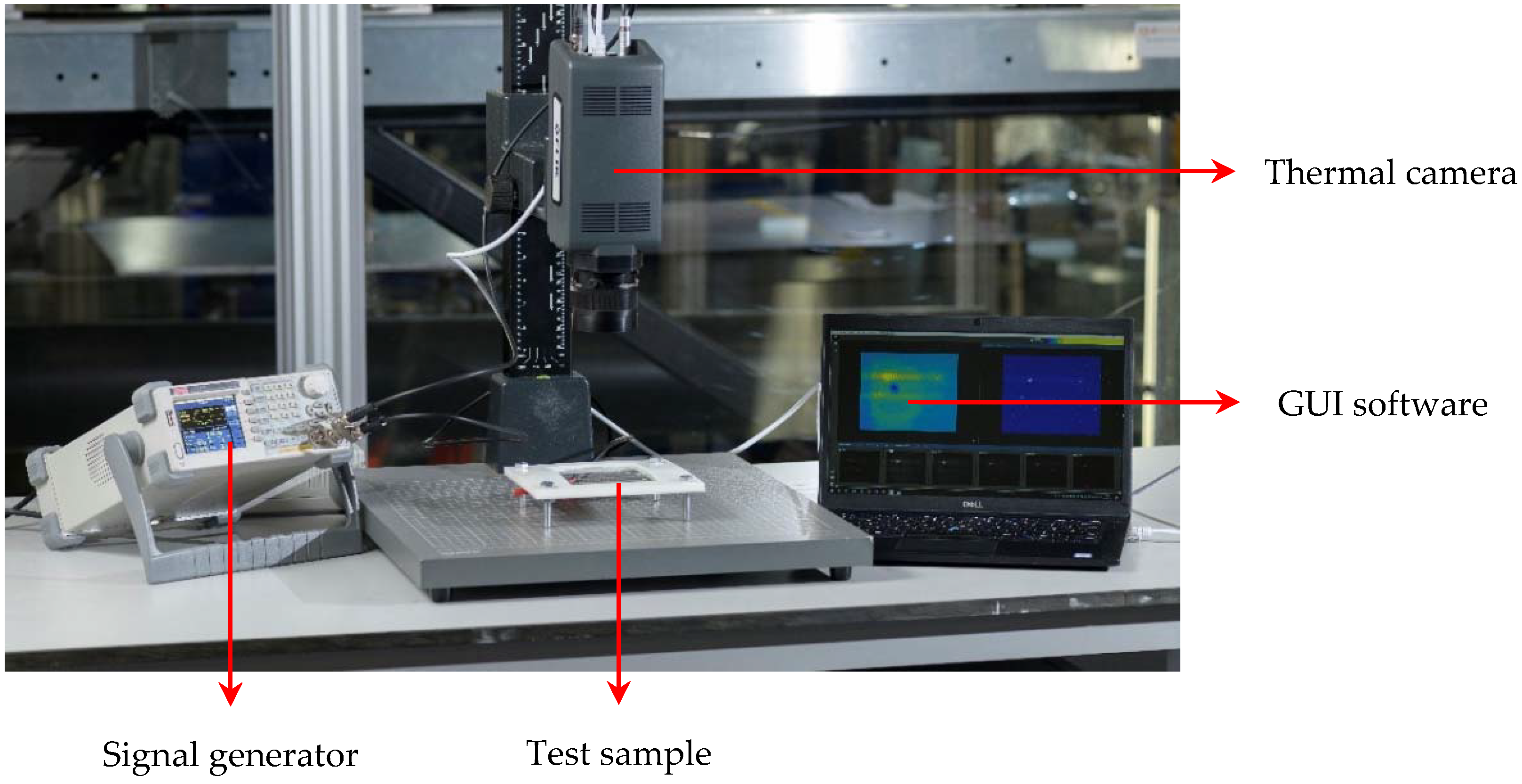
In the DLIT system, as shown in
Figure 1, a periodically modulated voltage is applied to the test sample while being imaged using an infrared thermal camera (FLIR A6751 MWIR F/2.5). This cooled indium antimonide (InSb) camera offers high-speed windowed frame rates (up to 120 Hz), performs a variety of non-destructive testing, and provides 327,680 (640 × 512) pixel resolution. Along with thermal images, the camera can also record the synchronized square wave reference signal that is generated using a signal generator (RS Pro RS DG805 Signal Generator). The in-house developed software comprises data acquisition, data visualization, lock-in post processing and data analysis capabilities through a graphical user-interface (GUI).
During the thermography test, the camera records the frames of thermal video images and the synchronized heating excitation simultaneously. In the lock-in correlation procedure, the frames are multiplied with the weight factors in two channels. The product of recorded frame and in-phase weight factor is summed over the entire dataset to provide the sine image
. On the other hand, the same process is repeated but with a 90° phase shifted quadrature weight factor resulting in a cosine image
. The amplitude of the temperature variation as well as the phase can be obtained from the two images produced [
20]. The post processing procedure is graphically illustrated in
Figure 2.
3. DLIT Trials
DLIT tests were carried out on the R2R printed thin film samples provided by VTT. The conductors are rotary screen-printed Ag-wires (Dupont 5025) on a polyethylene terephthalate (PET) foil (Melinex ST506) [
18].
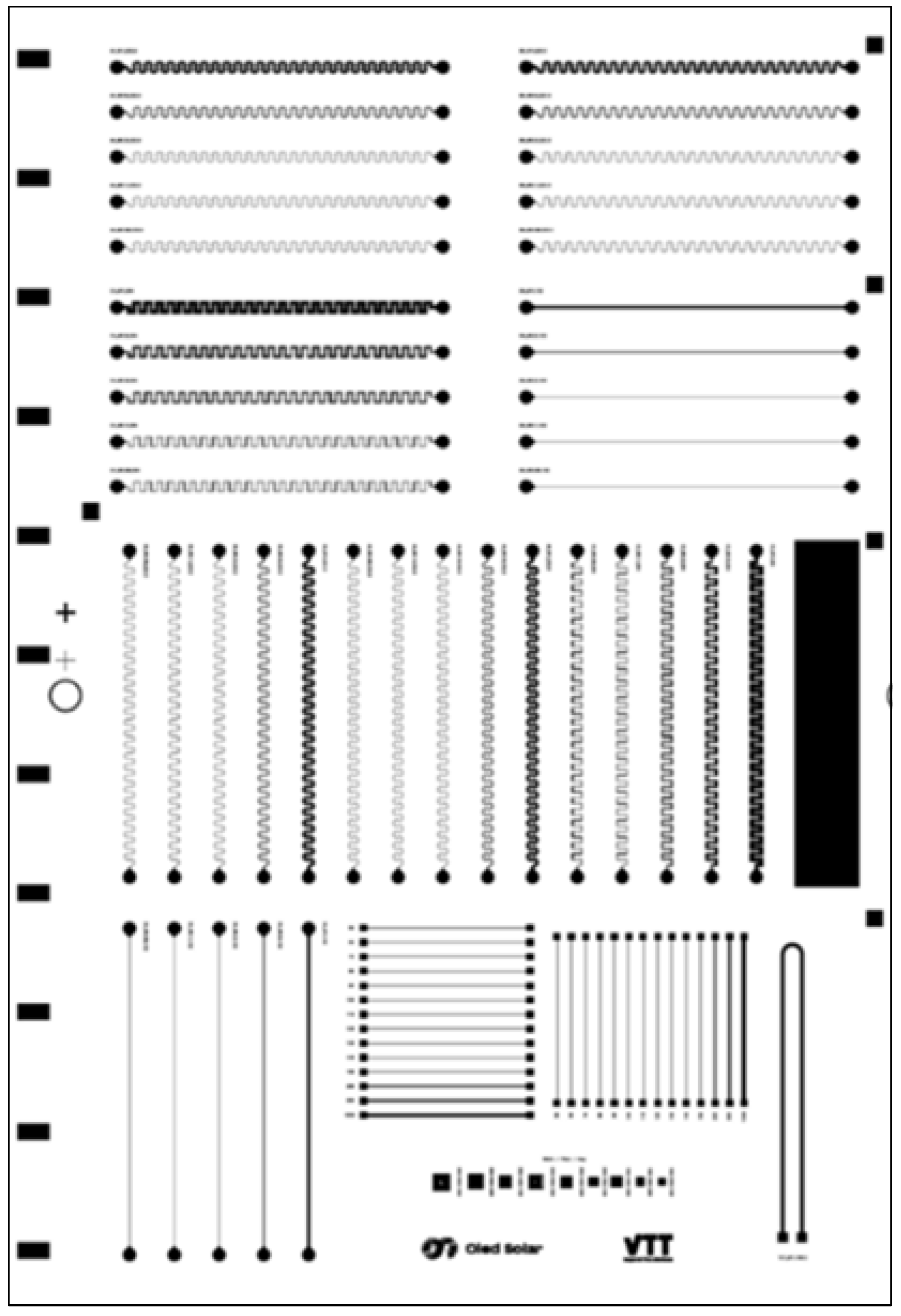
Figure 3 shows one piece of R2R printed silver conductor on PET foil.
To validate the developed DLIT system’s ability to identify electrical defects on the R2R printed thin film, the test sample was created by cutting a small piece of specific printing pattern with five printing wires (8 cm × 12 cm) from the full piece of printed thin film (
Figure 3).
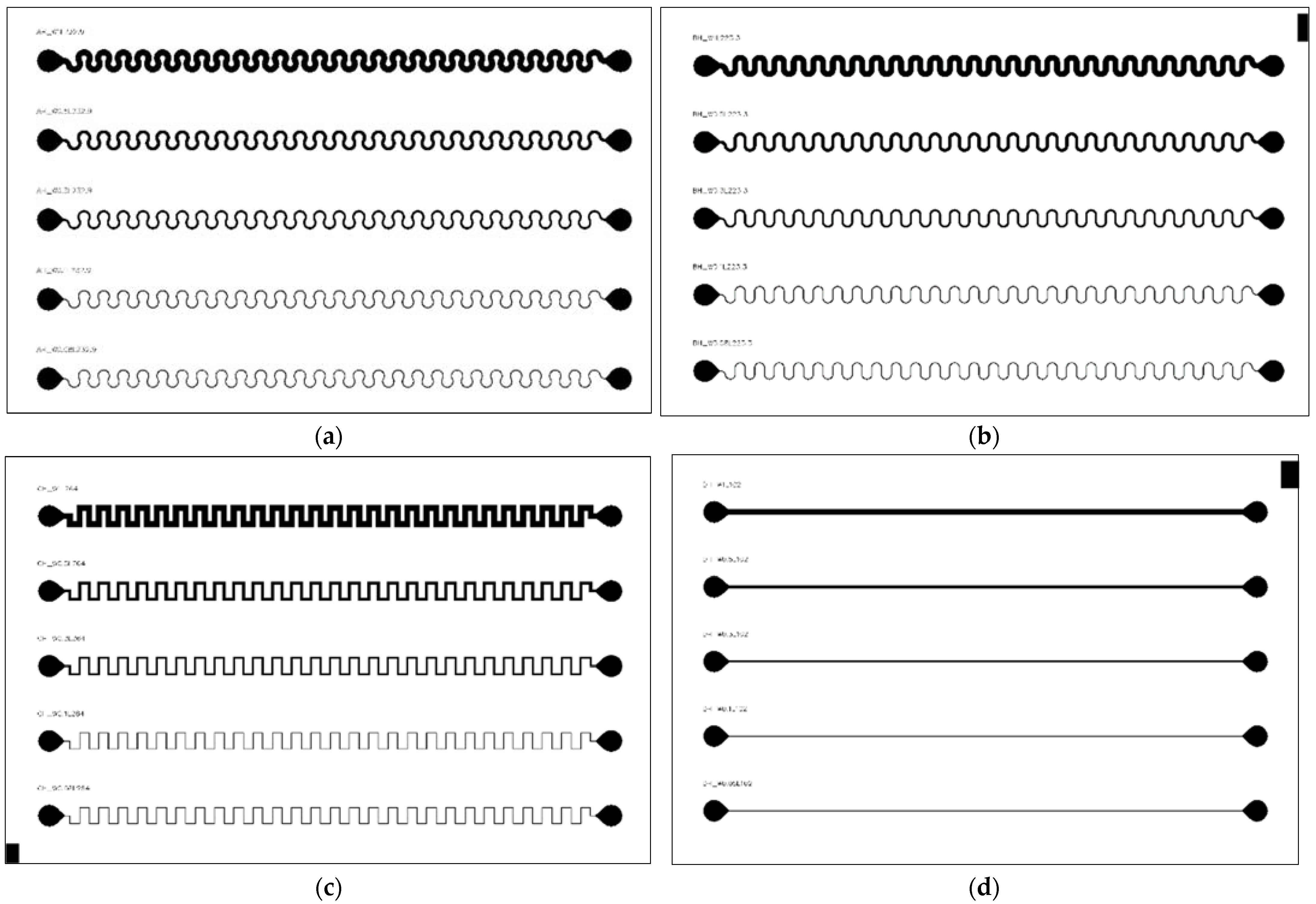
Figure 4a–d show the cropped single piece of test sample of four printing patterns to be used for laboratory trial. Four patterns (meander, U-shape, rectangular, straight) were R2R printed with different widths (80, 100, 300, 500, 1000 μm).
A test jig was specifically designed and additively consisted of a specimen holder that enables the application of voltage across five printed wires simultaneously using pogo pins. As shown in
Figure 5, a cropped test sample, with printing patterns of meander shape, was installed on the test jig. During DLIT test, two terminals were connected to the signal generator to apply 5 Ag-wires with 0–5 V square wave at 1 Hz. The infrared camera was set to record the data at 60 Hz for a period of 5 s.
Artificial defects were induced on the test samples to replicate defected printing. Two types of typical printing defects were considered in this study, which were:
Complete wire breaks—artificially created by cutting through the printed Ag-wire. The complete wire breaks result in open circuits so zero current can flow between the two terminals;
Partial wire breaks—artificially created by scratching and partially cutting the printed Ag-wire. The partial wire breaks result in a local increased resistance consequently a higher temperature to be detected by an infrared camera, which is so-called hot spot.
3.1. Defect Case 1—Complete Wire Breaks
Figure 6 shows the test samples with complete wire breaks, which were tested in the laboratory trials. Test sample 1, as shown in
Figure 6a, is a 5-wire thin film of U-shape printing pattern with a cut through defect on the third wire, which is in the middle of the thin film. Test sample 2, as shown in
Figure 6b, is a 5-wire thin film of straight printing pattern with a cut through defect on the fifth wire, which is at the bottom of the thin film. The defects and their locations are indicated in the enlarged images.
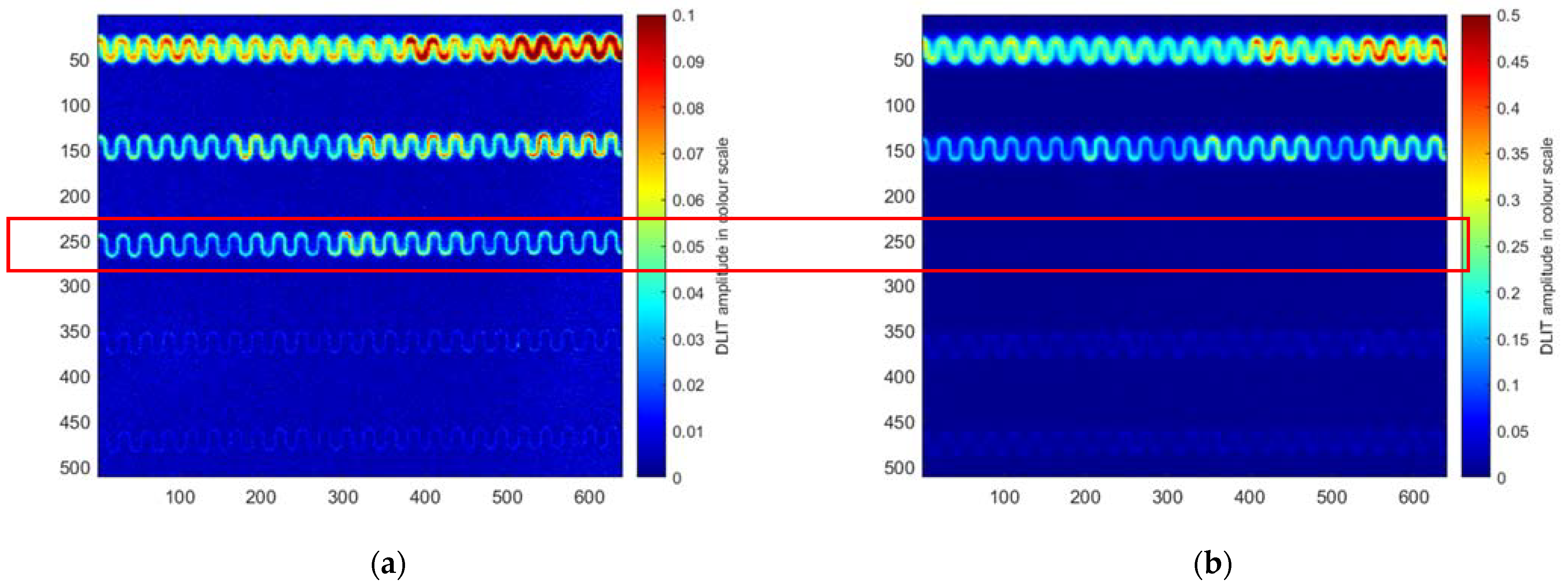
Figure 7 and
Figure 8 shows the processed DLIT amplitude images of two test samples.
Figure 7a,b show the results of Test Sample 1 without and with a complete wire broken. It can be seen that a complete wire break on the third wire prevents the wire from being illuminated so that it is invisible in the DLIT amplitude image, as highlighted by a red rectangle.
Figure 8a,b show the results of Test Sample 2 without and with a complete wire break. The broken wire, which is the fifth wire on Test Sample 2, is invisible in
Figure 8b, as highlighted by a red rectangle.
3.2. Defect Case 2—Partial Wire Breaks
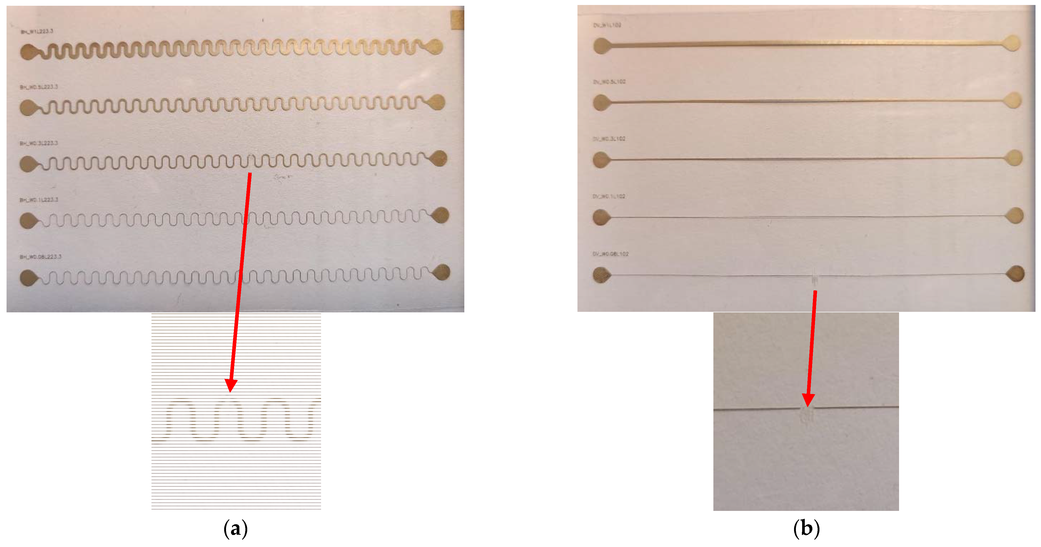
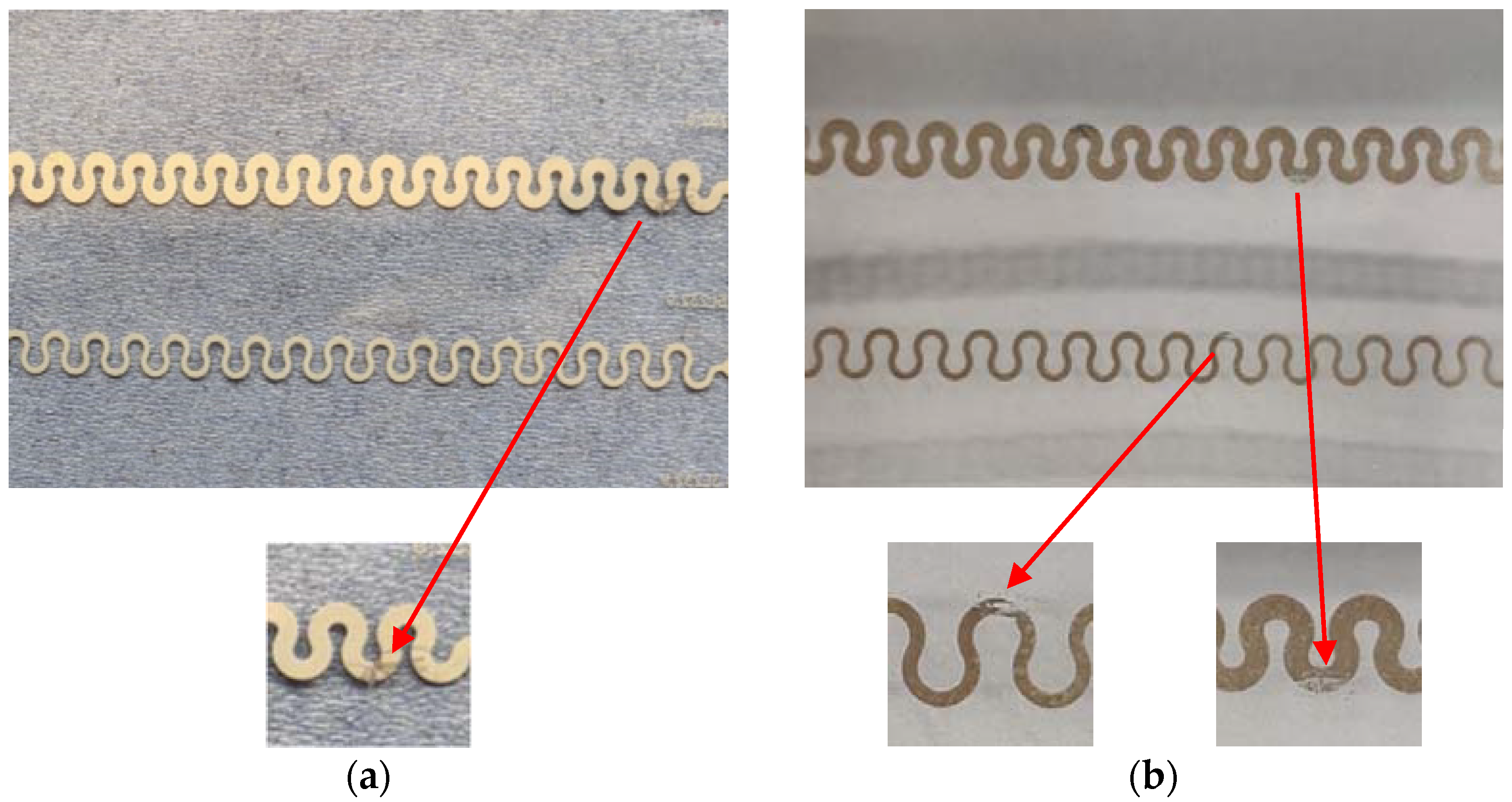
Figure 9 shows the test samples with partial wire breaks. A partial wire break was induced on Test Sample 3, as shown in
Figure 9a. Two partial wire breaks were induced on Test Sample 4, as shown in
Figure 9b. The arrows in red indicate the locations of the defects in the figures. The defect sizes of these two wire breaks are around a half of the wire widths, which are 250–500 μm.
Figure 10 shows the DLIT amplitude images of Test Samples 3 and 4. It is seen from the figures that the partial wire breaks can be clearly detected as hot spots, which are indicated by the arrows in red.
4. ADR Algorithms
As previously discussed, two types of typical defects on the conductive thin film were investigated in this study which have distinct characteristics captured by the DLIT method: namely, complete wire breaks, e.g.,
Figure 7b, and partial wire breaks such as the images shown in
Figure 10. An ADR algorithm can automate the detection process for the two defect types, therefore reducing the labor cost for human inspection and increasing the efficiency of monitoring R2R fabrication process.
For ADR development and processing, the amplitude matrices collected from the DLIT process are adopted and analyzed, instead of using the image formats presented in previous section. Adopting the data matrices grants access to raw pixels, hence facilitating detailed analysis. The input data are 512 × 640 matrices of pixel values from laboratory trials. To assist analysis, all input matrices are visualized in grayscale. An example is demonstrated in
Figure 11a below using data from Test Sample 1.
4.1. Challenges with DLIT Images
It has been shown in the previous section that the DLIT process can generate images with high signal-to-noise ratio (SNR) to facilitate operators to spot defects, e.g.,
Figure 10. However, the DLIT images also bring several challenges when dealing with region of interest (ROI) detection, which will be discussed in the following paragraphs.
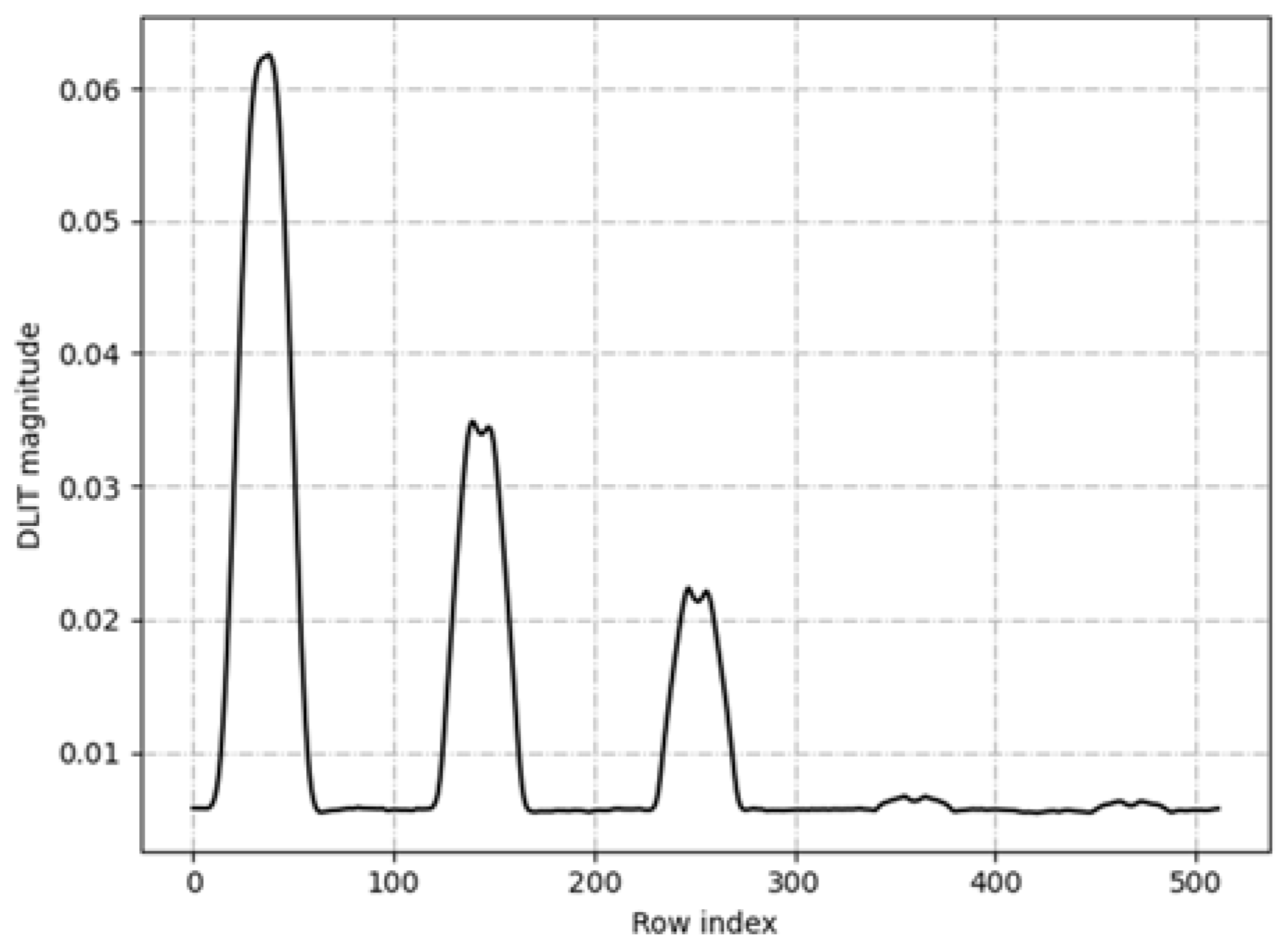
Firstly, the intensity of each wire is not uniform and should be investigated individually. For instance, it can be observed from
Figure 11b that the first three wires are clearly visible in grayscale, whereas the last two wires are not visible directly in grayscale, unless scaled as shown in
Figure 7a. In this paper, the overall intensity level for each wire is estimated by inspecting averaged pixel magnitude per row, calculated from the equation below:
where
r is the row number, and
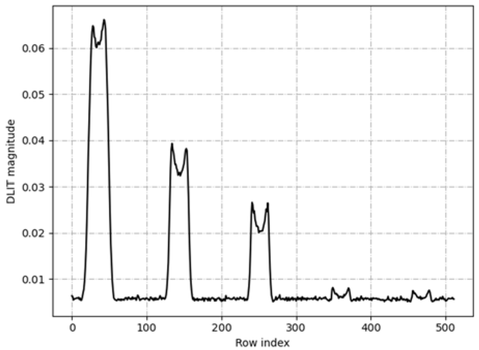
c represents the number of columns in the image. Note that because the images are generated using DLIT method, the pixels are dimensionless and are not actual temperature levels. In
Figure 12, an intensity estimation plot is presented, based on the data shown in
Figure 11, which were collected from a five-wire sample with no defects.
It is evident from
Figure 12 that the intensity level of the three wires (ROI from row 0 to 300) are clear. However, as the wire becomes thinner for the last two wires (ROI from row 300 to 500), the intensity level is barely noticeable in relation to the background. Additionally, the intensity curve within the edges of each wire resembles a “bathtub” curve, where the lowest intensity occurs in between the edges. This makes it more challenging to distinguish the thinner wires against the background noise, especially when applying traditional thresholding methods, such as Otsu’s method [
21]. Otsu’s method is effective in automatically choosing threshold to separate all the pixels into two classes, namely the foreground and background, but its efficacy deteriorates as the intensity of the thin wires tend to the values of background noise while the thick wires are distinctly stronger. Similarly, other widely adopted edge-based methods such as the Canny edge detector [
22] perform less effectively. The Canny edge detector is a multi-stage algorithm that discovers the intensity gradients of the image in both horizontal and vertical directions, and then applies thresholding to determine potential edges. It therefore suffers from lack of contrast in the weak edges. Although it is likely to achieve optimal edge detection results through fine-tuning of the Canny detector parameters including the width of Gaussian filter, the lower and upper threshold for hysteresis thresholding, but the process is tedious.
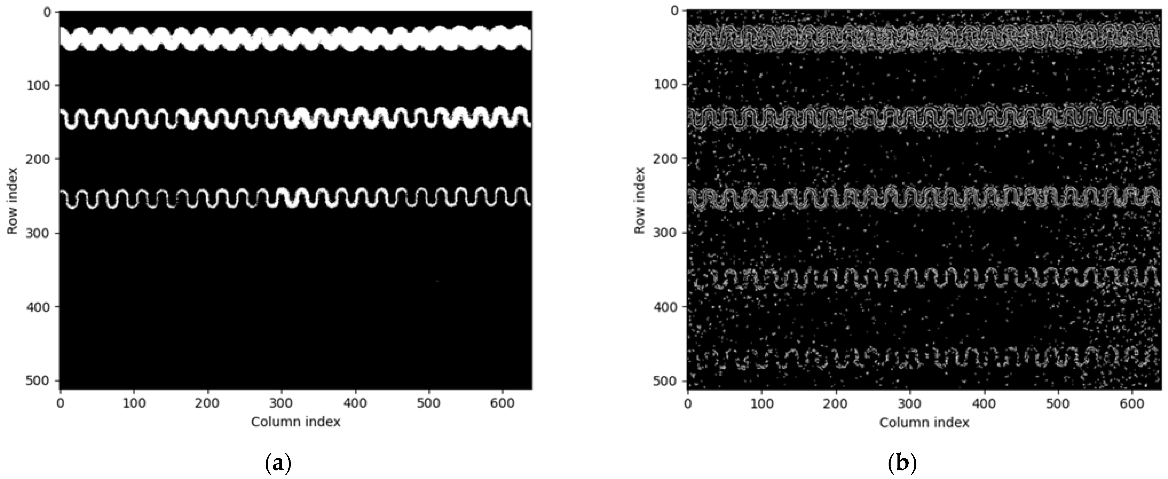
As shown in
Figure 13a, Otsu’s method separates the top three wires which are strong, but completely misses the two thin wires at the bottom. The Canny edge detector in
Figure 13b performs better where all five wires are detected, although some background noise persists. However, the process of finding the optimal parameters for the Canny edge detector are challenging, because the efficacy of the Canny edge detector is highly dependent on the low and high thresholding as well as the Gaussian filter used.
In addition to the thresholding and edge-based detection methods, there are other methods proposed based on various algorithms [
23,
24,
25,
26], such as region-based methods [
27], clustering-based methods [
28] and deep-learning methods [
29,
30,
31]. However, they all have their own drawbacks. The DLIT images are inherently one channel grayscale, therefore it is difficult to implement distance-based algorithms, e.g., clustering methods as the pixel space is only one dimension of intensity. Another challenge is that due to the difficulty in obtaining thin films with natural wire breaks, the number of images generated from experiments are not sufficient to support the training needs for deep-learning based methods. Therefore, in this study, a multi-stage image processing pipeline was developed, which consists of localized segmentation to extract areas of illuminated wires, and hot spot detection based on further analysis within the detected illuminated wire areas.
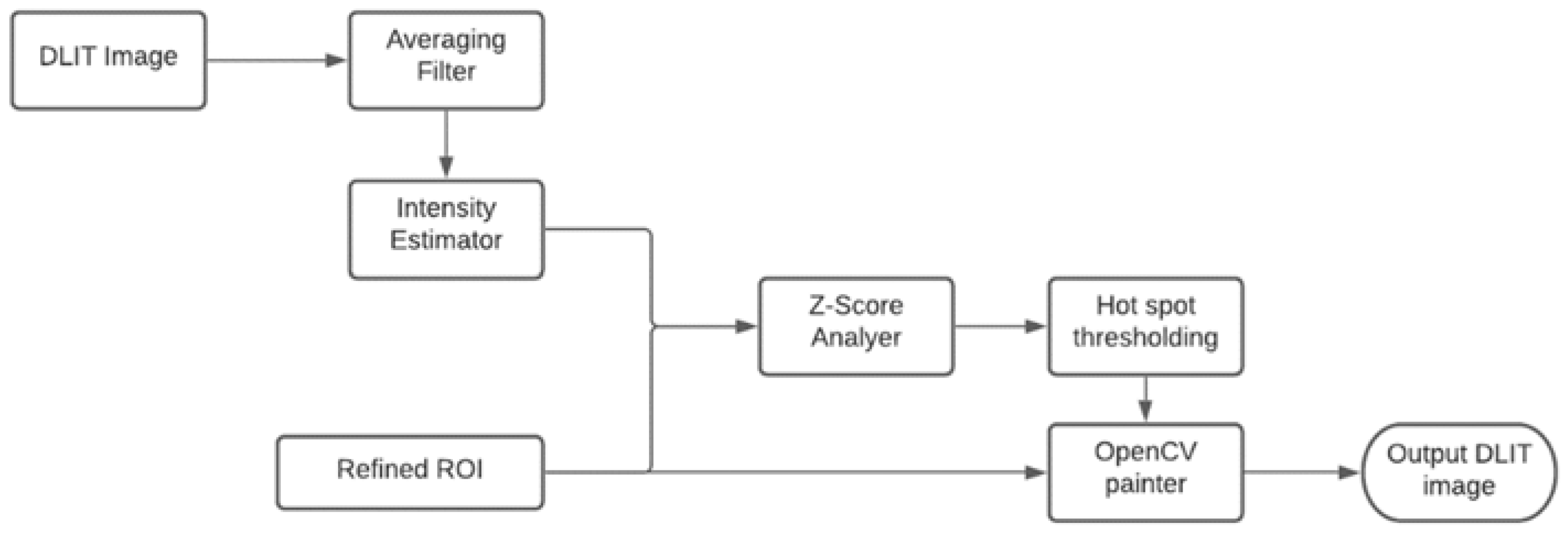
4.2. Localised Segmentation
To overcome the issue of weak intensity pixels, the ROI that contain wires are proposed be inspected locally and individually so that the weak signatures can be extracted in a refined ROI. The working principle of R2R and DLIT determines that the relative positions of the wires are fixed during inspection, making the localized inspection possible. The schematic diagram for this process is depicted in
Figure 14.
The averaging filter is applied as a first step to further remove any unwanted noise and minor fluctuations. For this study, it was discovered that a general 15 × 15 averaging filter was adequate. The intensity estimator plot shown in
Figure 15 demonstrates the smooth effect in comparison to the unprocessed intensity plot in
Figure 12. It is shown that the minor fluctuations are suppressed, as well as the “bathtub” curves in between the front and back edges for each wire.
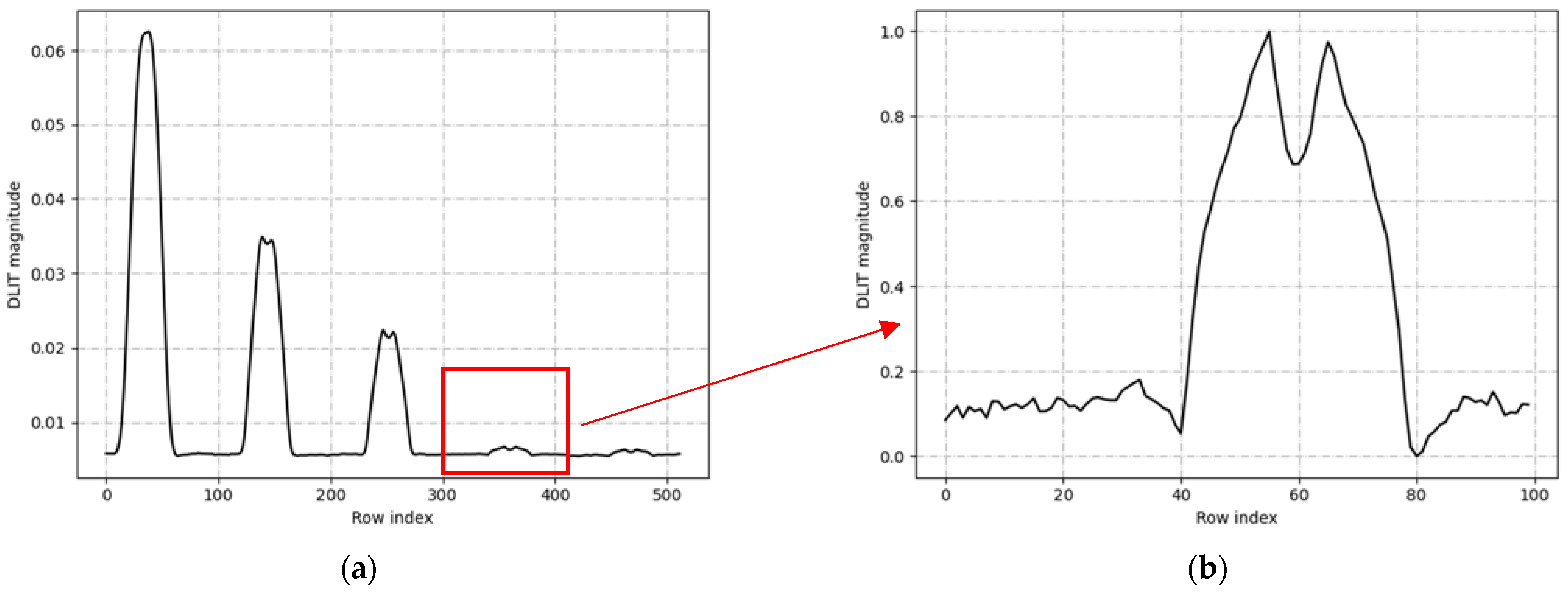
The next step was to extract the pixels within the specified a rough ROI individually so that a more refined ROI could be defined for wire detection. To achieve highlighting possible pixel peaks and reducing the pixel noises, a 0–1 scaler function was applied for each specified ROI. The 0–1 scaler was defined as a mapping function, which converts the pixel values from one range to range of [0, 1], so that the smaller pixels are suppressed and pixels with larger intensities are amplified. The scaler is achieved through the equation defined in Equation (4):
The effect of this 0–1 scaler is demonstrated in
Figure 16, where an example of rough ROI of [300–400] row index is given. It is worth noting that the 0–1 scaler itself does not modify the shape of the curve, but rather normalizes the DLIT image so that all pixels are comparable in the same scale of [0, 1] for the thresholding process.
From
Figure 16, a globally applicable threshold, in this study 0.4 can be applied to detect the edges using heuristic rules:
There should be other heuristics, including that the detected Back edge should come after the Front edge, the number of Front edges and Back edges should be equal, and multiple Front edges and Back edges should be allowed to be discovered in order to increase the sensitivity of weak signal detection. If after processing, no edges are discovered, satisfying the rules specified above, then it indicates no wire is detected in the specified ROI.
If edges are detected, the refined ROI is formed by combining earliest Front edge and latest Back edge. In the
Figure 16 example, the detected refined ROI is [342, 377], noted that the 300 offset is added on row index from
Figure 16b. The refined ROI is sent to a z-score analyzer to detect irregularities that are associated with hot spots.
4.3. Hot Spot Detection Based on Localised Segmentation
As shown in
Figure 17, the refined ROI is sent to a z-score analyzer, which then determines the existence of hot spots induced by partial wire breaks within the refined ROI.
The z-score analyzer analyses the z-score defined by the equation below:
where the s represents the standard deviation of the pixels. The z-score indicates how far away each pixel within the refined ROI is deviated from the mean value. If a hot spot exists within the ROI, then the z-scores for the pixels associated with hot spot will be severely deviated from normal pixels. The thresholding to determine the existence of hot spot in this paper is set to z-score of six, acquired from DLIT images obtained from lab-based experiments.
If the hot spots are detected, the corresponding ROI will be painted as red using a painter provided by OpenCV library. If not detected, the corresponding ROI will be painted as green. In spite of whether hot spots are detected, all detected refined ROI will be counted into the number of wires detected.
5. ADR Results and Discussion
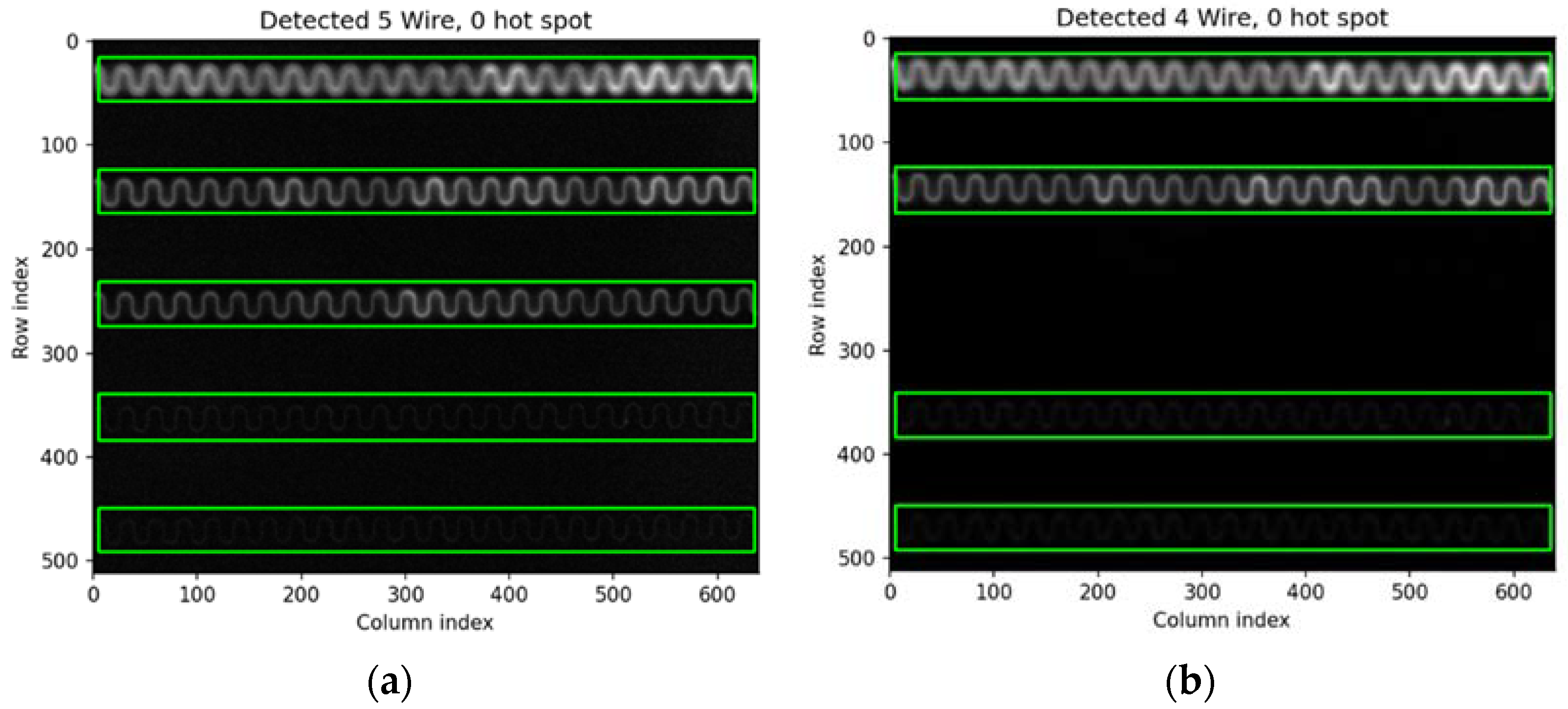
The DLIT images introduced in Chapter 3—DLIT Trials, were used for validating the proposed two-stage method. In
Figure 18 and
Figure 19, the DLIT images of thin film Test Sample 1 and Test Sample 2 with and without wire breaks, which are shown previously in
Figure 7 and
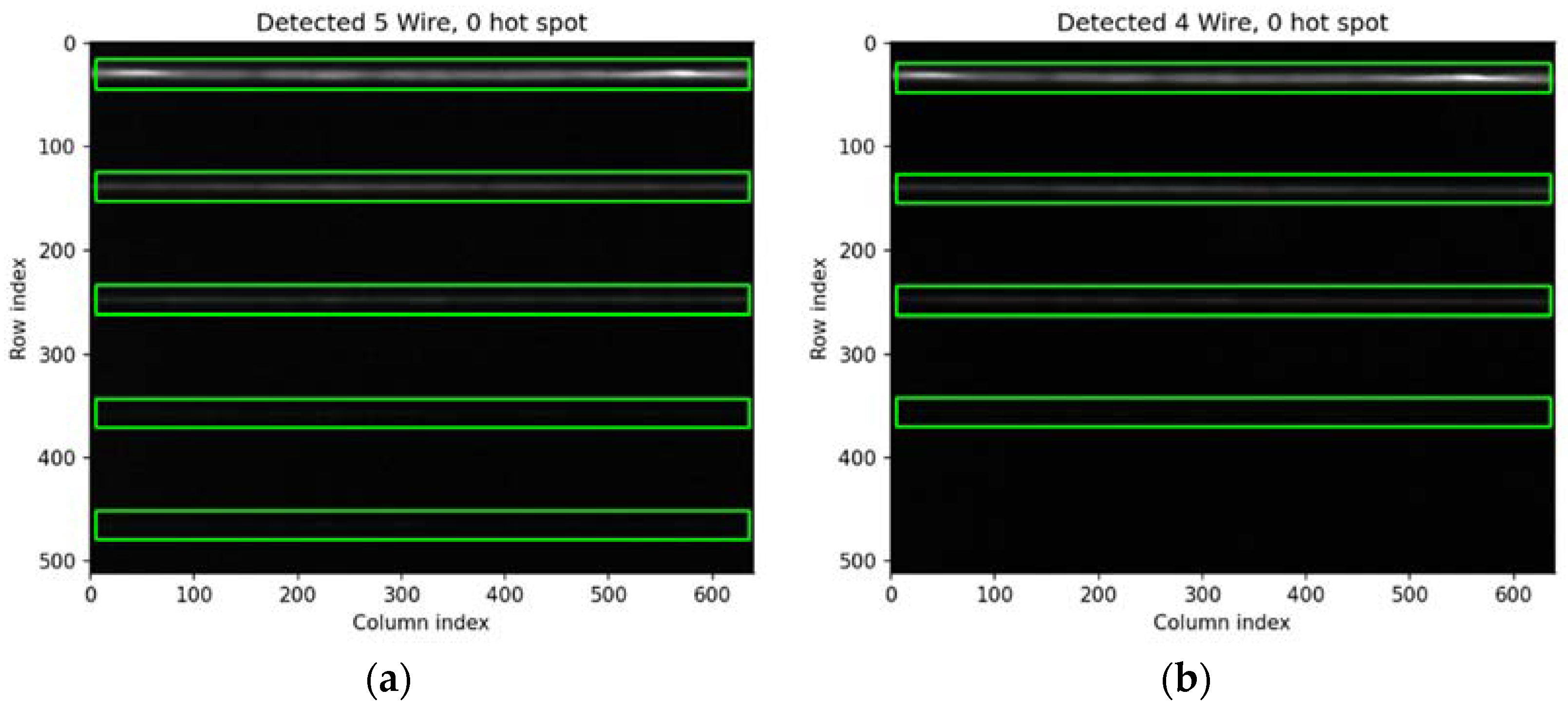
Figure 8, are processed. The wires are U-shaped and straight-line shaped, respectively. No hot spots were instigated or detected in this batch of results, which is in line with the prior knowledge that no hot spots existed in these samples.
It is evident that in
Figure 18, the refined ROI areas are successfully detected and clearly highlighted in green for both types of wires with an intention of assisting confirmation checks. After processing, weak wires such as the bottom two wires shown in
Figure 19a, which can barely be seen with naked eyes, are detected and highlighted to avoid being mistakenly classified as breaks. Additionally, the detection results are automatically labelled as image titles. The results can also be summarized in batches to assist operators’ post inspection.
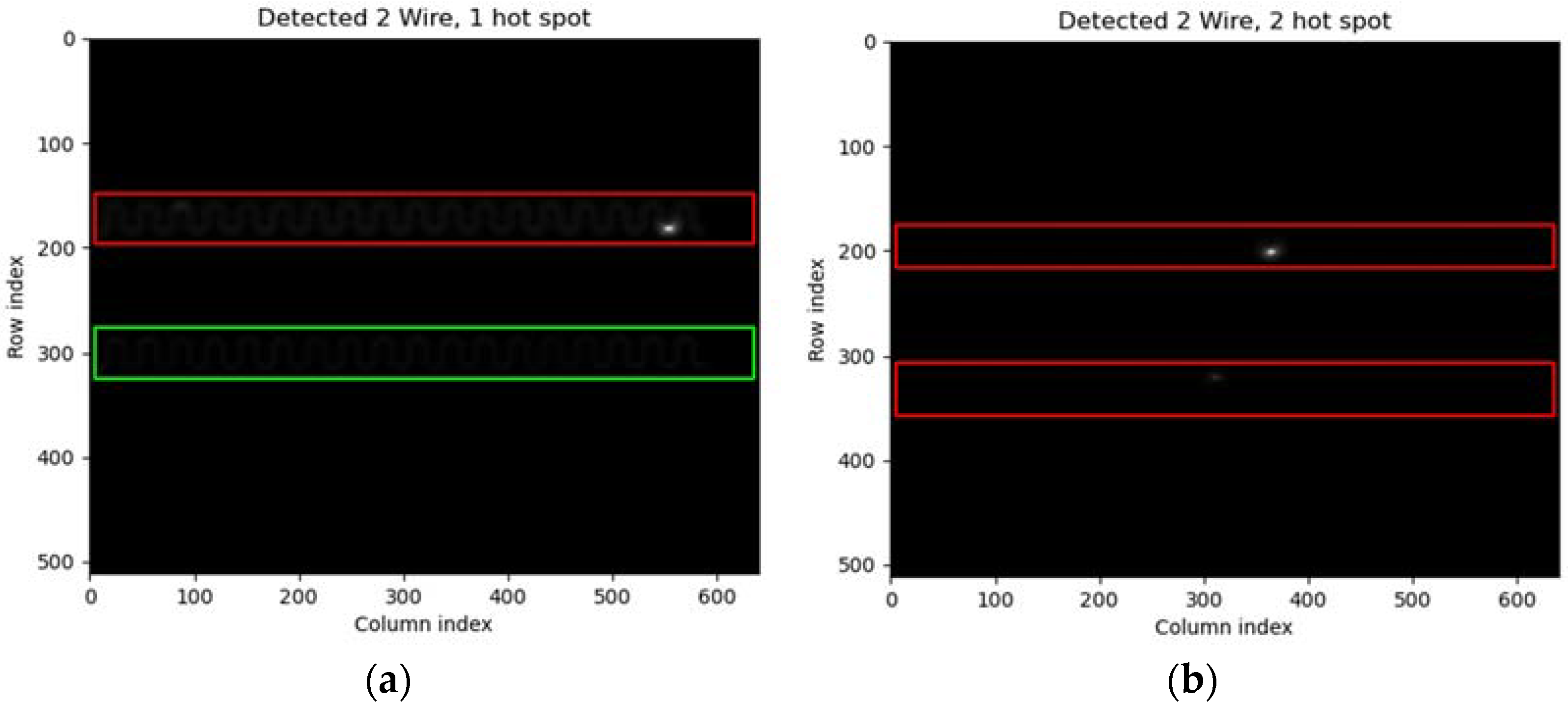
In
Figure 20, the DLIT images of thin film Test Sample 3 and Test Sample 4 with partial wire breaks, which were previously shown in
Figure 10, were processed. It is clear that the ROI contains hot spots which are correctly highlighted in red color, whereas normal wires are labelled in green color.
The ADR results presented in figures from
Figure 19 to
Figure 20 show that the developed ADR algorithm is able to successfully detect the ROI of intact wires, detect wires with hot spots, and detect complete wire breaks. Detected intact wires’ ROIs are highlighted with green frames, whereas wires with hot spots are highlighted with red frames. Number of complete wire breaks can be calculated by subtracting number of wires detected from total number of wires. The entire process is automatically completed by the processing computer with a pre-defined coarse ROI arrangement of wires, and the detection results can be incorporated into a separate reporting system to generate batch processing results for human operators, or with an alarm system which notifies operators when wire breaks or hot spots are detected.
The ADR algorithm, written in Python, runs 0.7 s processing time per image, on a laptop with 16GB RAM and an Intel i7 processor. The ADR can be further optimized using compiled programming languages such as C/C++ to reduce processing time. The short processing time required means that the ADR is suitable to operate either as an in-line inspection tool to be incorporated into the DLIT system, or as a post-analysis tool to assist post-inspection of the fabricated films.
The current version of ADR is semi-automatic as it still requires the operators to input a coarse ROI arrangement of wires. To be able to achieve full-automatic ADR, additional experiment data need to be collected to enable edge detection and image object segmentation using Deep Learning methods to detect the coarse ROI as input to the proposed ADR. Simulation work has been undertaken to generate bespoke images to be used as training datasets.
6. Conclusions
A DLIT tool was developed to inspect R2R printed silver conductors on thin films. It has been shown that it has the ability to detect defects in the printing quality of printed patterns in this study, which will help the operator to find the faulty parts in the roll and remove them before further processing. When compared to simple resistance measurements, the benefit of DLIT is that, in addition to showing that the conductor is faulty/not conducting, it shows exactly the position of the defect, which will help to improve the printing process in the following runs. This will improve the production yield and reduce the amount of waste.
To enable ADR for identifying the type and location of defects from DLIT images, a multi-stage image processing methodology was proposed based on localized segmentation and thresholding. The results of ADR processing of DLIT images are promising, although they were demonstrated on limited laboratory trial results. The DLIT tests were run semi-automatically by manually initiating thermal image acquisition and post-processing. In the next stage, the DLIT tool will be upgraded to provide fully automated operation and implemented on R2R testing line at VTT to continually inspect the printed conductive thin films. The future works will also include more DLIT trials with various printing pattern, material, and defect scenarios. Hence, the repeatability and robustness of the proposed method can be extensively studied in the next stage.
Author Contributions
Conceptualization, H.Z., L.Z., R.M., T.M.K. and T.H.; methodology, H.Z. and L.Z.; software, H.Z. and L.Z.; experimental validation, H.Z. and T.H.; writing—original draft preparation, H.Z. and L.Z.; reviewing, R.M., T.H. and T.M.K.; project administration, R.M. and T.M.K. All authors have read and agreed to the published version of the manuscript.
Funding
The OLEDSOLAR project has received funding from the European Union’s Horizon 2020 under grant agreement number 820789.
Institutional Review Board Statement
Not applicable.
Informed Consent Statement
Not applicable.
Conflicts of Interest
The authors declare no conflict of interest.
References
- Søndergaard, R.R.; Hösel, M.; Krebs, F.C. Roll-to-Roll fabrication of large area functional organic materials. J. Polym. Sci. B Polym. Phys. 2013, 51, 16–34. [Google Scholar] [CrossRef]
- Van De Wiel, H.J.; Galagan, Y.; Van Lammeren, T.J.; De Riet, J.F.J.; Gilot, J.; Nagelkerke, M.G.M.; Lelieveld, R.H.C.A.T.; Shanmugam, S.; Pagudala, A.; Hui, D.; et al. Roll-to-roll embedded conductive structures integrated into organic photovoltaic devices. Nanotechnology 2013, 24, 484014. [Google Scholar] [CrossRef]
- Hösel, M.; Angmo, D.; Søndergaard, R.R.; dos, G.A.; Benatto, R.; Carlé, J.E.; Jørgensen, M.; Krebs, F.C. High-volume processed, ito-free superstrates and substrates for roll-to-roll development of organic electronics. Adv. Sci. 2014, 1, 154–196. [Google Scholar] [CrossRef] [Green Version]
- Abbel, R.; Galagan, Y.; Groen, P. Roll-to-Roll Fabrication of Solution Processed Electronics. Adv. Electron. Mater. 2018, 20, 1–30. [Google Scholar] [CrossRef] [Green Version]
- Schwartz, E. Roll to Roll Processing for Flexible Electronics. Master’s Thesis, Cornell University, Ithaca, NY, USA, 11 May 2006. [Google Scholar]
- Sumaiya, S.; Kardel, K.; El-Shahat, A. Organic Solar Cell by Inkjet Printing—An Overview. Technologies 2017, 5, 53. [Google Scholar] [CrossRef] [Green Version]
- Palavesam, N.; Marin, S.; Hemmetzberger, D.; Landesberger, C.; Bock, K.; Kutter, C. Roll-to-roll processing of film substrates for hybrid integrated flexible electronics. Flex. Print. Electron. 2018, 3, 014002. [Google Scholar] [CrossRef]
- Søndergaard, R.; Hösel, M.; Angmo, D.; Larsen-Olsen, T.T.; Krebs, F.C. Roll-to-roll fabrication of polymer solar cells. Mater. Today 2012, 15, 36–49. [Google Scholar] [CrossRef] [Green Version]
- OledSolar. Available online: https://oledsolarproject.eu (accessed on 2 February 2022).
- OLEDSOLAR Completes Inspection and Quality Control Work. Available online: https://www.twi-global.com/media-and-events/press-releases/2021/oledsolar-completes-inspection-and-quality-control-work (accessed on 2 February 2022).
- Apilo, P. Roll-to-Roll Printing of Organic Photovoltaic Cells and Modules. Ph.D. Thesis, VTT Technical Research Centre of Finland, Oulu, Finland, 9 June 2015. [Google Scholar]
- Hoppe, H.; Bachmann, J.; Muhsin, B.; Drüe, K.H.; Riedel, I.; Gobsch, G.; Buerhop-Lutz, C.; Brabec, C.J.; Dyakonov, V. Quality control of polymer solar modules by lock-in thermography. J. Appl. Phys. 2010, 107, 014505. [Google Scholar] [CrossRef]
- Rösch, R.; Krebs, F.C.; Tanenbaum, D.M.; Hoppe, H. Quality control of roll-to-roll processed polymer solar modules by complementary imaging methods. Sol. Energy Mater. Sol. Cells 2012, 97, 176–180. [Google Scholar] [CrossRef]
- Reinhardt, J.; Apilo, P.; Zimmermann, B.; Rousu, S.; Würfel, U. Determining the photocurrent of individual cells within an organic solar module by LBIC and the filtering approach: Experiments and simulations. Sol. Energy Mater. Sol. Cells 2015, 134, 157–164. [Google Scholar] [CrossRef]
- Sekine, C.; Tsubata, Y.; Yamada, T.; Kitano, M.; Doi, S. Recent progress of high performance polymer OLED and OPV materials for organic printed electronics. Sci. Technol. Adv. Mater. 2014, 15, 034203. [Google Scholar] [CrossRef] [PubMed]
- Logothetidis, S.; Georgiou, D.; Laskarakis, A.; Koidis, C.; Kalfagiannis, N. In-line spectroscopic ellipsometry for the monitoring of the optical properties and quality of roll-to-roll printed nanolayers for organic photovoltaics. Sol. Energy Mater. Sol. Cells 2013, 112, 144–156. [Google Scholar] [CrossRef]
- Espinosa, N.; Lenzmann, F.O.; Ryley, S.; Angmo, D.; Hösel, M.; Søndergaard, R.R.; Huss, D.; Dafinger, S.; Gritsch, S.; Kroon, J.M.; et al. OPV for mobile applications: An evaluation of roll-to-roll processed indium and silver free polymer solar cells through analysis of life cycle, cost and layer quality using inline optical and functional inspection tools. J. Mater. Chem. A 2013, 1, 7037–7049. [Google Scholar] [CrossRef] [Green Version]
- Happonen, T.; Tuomikoski, M.; Kokko, T.; Ronka, K. Roll-to-roll functional testing of printed conductors and organic light emitting devices. In Proceedings of the 2018 7th Electronic System-Integration Technology Conference (ESTC), Dresden, Germany, 18–21 September 2018; pp. 1–5. [Google Scholar] [CrossRef]
- Happonen, T.; Kokko, T.; Juntunen, E.; Rönkä, K. Quality assurance for rotary screen printed wiring backplanes with automated roll-to-roll electrical test equipment. Flex. Print. Electron. 2019, 4, 025002. [Google Scholar] [CrossRef]
- Breitenstein, O.; Warta, W.; Schubert, M.C. Lock-in Thermography: Basics and Use for Evaluating Electronic Devices and Materials, 3rd ed.; Springer: Berlin/Heidelberg, Germany, 2018. [Google Scholar]
- Otsu, N. A threshold selection method from gray-level histograms. IEEE Trans. Syst. Man Cybern. 1979, 9, 62–66. [Google Scholar] [CrossRef] [Green Version]
- Canny, J. A computational approach to edge detection. IEEE Trans. Pattern Anal. Mach. Intell. 1986, PAMI-8, 679–698. [Google Scholar] [CrossRef]
- Kumar, S.N.; Fred, A.L.; Varghese, P.S. An overview of segmentation algorithms for the analysis of anomalies on medical images. J. Intell. Syst. 2020, 29, 612–625. [Google Scholar] [CrossRef]
- Lin, C.; Li, Y.; Feng, S.; Huang, M. A Two-Stage Algorithm for the Detection and Removal of Random-Valued Impulse Noise Based on Local Similarity. IEEE Access 2020, 8, 222001–222012. [Google Scholar] [CrossRef]
- Xing, F.; Cornish, T.C.; Bennett, T.; Ghosh, D.; Yang, L. Pixel-to-pixel learning with weak supervision for single-stage nucleus recognition in Ki67 images. IEEE Trans. Biomed. Eng. 2019, 66, 3088–3097. [Google Scholar] [CrossRef]
- Yuheng, S.; Hao, Y. Image segmentation algorithms overview. arxiv 2017, arXiv:1707.02051. [Google Scholar]
- Lalaoui, L.; Mohamadi, T. A comparative study of image region-based segmentation algorithms. Int. J. Adv. Comput. Sci. Appl. 2013, 4, 198–206. [Google Scholar] [CrossRef] [Green Version]
- Dhanachandra, N.; Manglem, K.; Chanu, Y.J. Image segmentation using K-means clustering algorithm and subtractive clustering algorithm. Procedia Comput. Sci. 2015, 54, 764–771. [Google Scholar] [CrossRef] [Green Version]
- Ghosh, S.; Das, N.; Das, I.; Maulik, U. Understanding deep learning techniques for image segmentation. ACM Comput. Surv. 2019, 52, 1–35. [Google Scholar] [CrossRef] [Green Version]
- Wang, G.; Li, W.; Zuluaga, M.A.; Pratt, R.; Patel, P.A.; Aertsen, M.; Vercauteren, T. Interactive medical image segmentation using deep learning with image-specific fine tuning. IEEE Trans. Med. Imaging 2018, 37, 1562–1573. [Google Scholar] [CrossRef] [PubMed]
- Minaee, S.; Boykov, Y.Y.; Porikli, F.; Plaza, A.J.; Kehtarnavaz, N.; Terzopoulos, D. Image segmentation using deep learning: A survey. IEEE Trans. Pattern Anal. Mach. Intell. 2021. [Google Scholar] [CrossRef] [PubMed]
Figure 1.
DLIT system set-up.
Figure 1.
DLIT system set-up.
Figure 2.
Lock-in processing of thermal images.
Figure 2.
Lock-in processing of thermal images.
Figure 3.
R2R printed silver conductor on PET foil.
Figure 3.
R2R printed silver conductor on PET foil.
Figure 4.
Cropped test sample with printing patterns (a) meander; (b) U-shape; (c) rectangular; (d) straight.
Figure 4.
Cropped test sample with printing patterns (a) meander; (b) U-shape; (c) rectangular; (d) straight.
Figure 5.
Test sample installed on test jig.
Figure 5.
Test sample installed on test jig.
Figure 6.
Complete wire breaks on (a) Test sample 1—U-shape printing pattern with cut through on the third wire; (b) Test sample 2—Straight printing pattern test sample with cut through on the fifth wire.
Figure 6.
Complete wire breaks on (a) Test sample 1—U-shape printing pattern with cut through on the third wire; (b) Test sample 2—Straight printing pattern test sample with cut through on the fifth wire.
Figure 7.
DLIT amplitude images of Test Sample 1 (a) without complete wire break; (b) with a complete wire broken on the third wire.
Figure 7.
DLIT amplitude images of Test Sample 1 (a) without complete wire break; (b) with a complete wire broken on the third wire.
Figure 8.
DLIT amplitude images of Test Sample 2 (a) without complete wire break; (b) with a complete wire broken on the fifth wire.
Figure 8.
DLIT amplitude images of Test Sample 2 (a) without complete wire break; (b) with a complete wire broken on the fifth wire.
Figure 9.
Partial wire breaks on (a) Test Sample 3—meander printing pattern with one partial wire break on the third wire; (b) Test Sample 4—meander printing pattern test sample with cut through on the fifth wire.
Figure 9.
Partial wire breaks on (a) Test Sample 3—meander printing pattern with one partial wire break on the third wire; (b) Test Sample 4—meander printing pattern test sample with cut through on the fifth wire.
Figure 10.
DLIT amplitude images of (a) Test Sample 3 and (b) Test Sample 4.
Figure 10.
DLIT amplitude images of (a) Test Sample 3 and (b) Test Sample 4.
Figure 11.
Demonstration of input data matrix for ADR and its visualization: (a) Input data matrix example, precision set to 2 significant decimals; (b) The corresponding visualization of (a) in grayscale.
Figure 11.
Demonstration of input data matrix for ADR and its visualization: (a) Input data matrix example, precision set to 2 significant decimals; (b) The corresponding visualization of (a) in grayscale.
Figure 12.
Demonstration of intensity estimate per row based on data shown in
Figure 11.
Figure 12.
Demonstration of intensity estimate per row based on data shown in
Figure 11.
Figure 13.
Demonstration of edge detection methods: (a) Otsu’s method; (b) Canny edge detector with sigma = 0.1, threshold = [0.025, 0.03].
Figure 13.
Demonstration of edge detection methods: (a) Otsu’s method; (b) Canny edge detector with sigma = 0.1, threshold = [0.025, 0.03].
Figure 14.
Schematic diagram of the process to refine ROI.
Figure 14.
Schematic diagram of the process to refine ROI.
Figure 15.
Intensity plot after applying 15 × 15 average filter.
Figure 15.
Intensity plot after applying 15 × 15 average filter.
Figure 16.
Effectiveness of 0-1 scaler: (a) Intensity plot prior to scaler; (b) Scaled area within ROI of [300, 400].
Figure 16.
Effectiveness of 0-1 scaler: (a) Intensity plot prior to scaler; (b) Scaled area within ROI of [300, 400].
Figure 17.
Schematic diagram of hot spot detection and ROI drawing.
Figure 17.
Schematic diagram of hot spot detection and ROI drawing.
Figure 18.
Demonstration of the wire breaks detection using the proposed method of Test Sample 1: (a) healthy condition of U-shaped wires; (b) one wire break in U-shaped wires.
Figure 18.
Demonstration of the wire breaks detection using the proposed method of Test Sample 1: (a) healthy condition of U-shaped wires; (b) one wire break in U-shaped wires.
Figure 19.
Demonstration of the wire breaks detection using the proposed method of Test Sample 2: (a) healthy condition of straight wires; (b) one wire break in straight wires.
Figure 19.
Demonstration of the wire breaks detection using the proposed method of Test Sample 2: (a) healthy condition of straight wires; (b) one wire break in straight wires.
Figure 20.
Hot spots detection on meander-shaped wires: (a) two wires with one hot spot (b) two wires with two hot spots.
Figure 20.
Hot spots detection on meander-shaped wires: (a) two wires with one hot spot (b) two wires with two hot spots.
| Publisher’s Note: MDPI stays neutral with regard to jurisdictional claims in published maps and institutional affiliations. |
© 2022 by the authors. Licensee MDPI, Basel, Switzerland. This article is an open access article distributed under the terms and conditions of the Creative Commons Attribution (CC BY) license (https://creativecommons.org/licenses/by/4.0/).


