
Study on Two-Dimensional Exit Pupil Expansion for Diffractive Waveguide Based on Holographic Volume Grating

Holographic Optics Lab, School of Physical Science and Technology, Xiamen University, Xiamen 361005, China
*
Author to whom correspondence should be addressed.
†
These authors contributed equally to this work.
Appl. Sci. 2023, 13(21), 11858; https://0-doi-org.brum.beds.ac.uk/10.3390/app132111858
Submission received: 18 September 2023
/
Revised: 18 October 2023
/
Accepted: 24 October 2023
/
Published: 30 October 2023
(This article belongs to the Collection Optical Design and Engineering)
Abstract
:Diffraction gratings are becoming a preferred option for waveguide head-mounted in–out coupling devices due to their flexible optical properties and small size and light weight. At present, diffraction waveguide coupling devices for AR head-mounted displays (HMD) have difficulties such as a long development cycle and complicated processing. In this paper, we first establish a set of two-dimensional (2D) grating ray tracing models, based on which we determine the initial architecture of the dual-region two-dimensional exit pupil expansion (2D-EPE) AR-HMD holographic waveguide diffraction system. Second, we propose a honeycomb coupled grating array and optimize the optical energy utilization and brightness uniformity of the holographic waveguide and use a custom dynamic linked library (DLL) function to implement the ray tracing of the 2D grating and add a probabilistic splitting function to the DLL, which reduces the single simulation time from 11.853 min to 1.77 min. We also propose a holographic lithography device composed of holographic optical elements (HOEs) and a method for preparing HOEs. Finally, in order to obtain the diffraction efficiency preoptimized by the above DLL for the uniformity of the exit pupil brightness and light energy utilization, we inverse design with the preparation process parameters as the optimization variables and develop the adaptable electromagnetic calculation program Holo-RCWA. Using Holo-RCWA with nondominated sorting genetic algorithm II (NSGA-II), we inverse design to obtain the process parameters satisfying the diffraction efficiency distribution, and the optimization time of the whole system is reduced from 2–3 days to 10 h. This work is of great significance for AR/VR applications.
1. Introduction
At present, diffractive waveguide based AR-HMD is favored by the market and consumers for its compact structure, low color crosstalk, high transparency, and low pupil swing distortion. The diffraction waveguide display system uses a microdisplay as the image source, collimates the light from the image source using a collimation system, couples the collimated light into the waveguide transmission medium through a coupling-in element, and, finally, transmits the image to the human eye through a coupling-out element. The coupling element directly influences the field of view (FOV), eyebox, and imaging brightness of an AR-HMD in a diffractive waveguide system. In practice, the coupling elements of diffractive waveguides are holographic gratings, surface relief grating (SRG), polarization volume grating (PVG), and super surface [1,2,3,4]. For example, Sony LMX-001 smart glasses (SONY, Tokyo, Japan) use reflective holographic grating, Digilens (Digilens, Sunnyvale, CA, America) uses volume holographic grating, and Hololens 2 (Microsoft, Redmond, WA, America) and Magic Leap One (Magic Leap, Plantation, FL, America) both use surface relief grating [5,6,7].
Eyebox is a key parameter in the design of HMD devices; the larger the geometry of the eyebox, the greater the range of motion of the human eye and the better the wearing experience for the user. Waveguide eyebox enlargement is achieved with the help of EPE. In order to reduce the impact of the input optical system on the overall size and weight of the HMD, it is necessary to expand the pupil in two directions. The basic structure of 2D-EPE has been theoretically determined [8], and Microsoft’s Hololens 1 adopts an “L-shaped” architecture [9,10], in which the grating periods of the coupled-in and coupled-out grating and the deflected grating are not parallel in the waveguide plane, enabling pupil expansion in two directions. WaveOptics uses a 2D grating as the coupling grating, which has two degrees of freedom in the grating vector, combining the functions of both the deflection grating and the coupling grating in the “L-shaped” architecture, while the waveguide size can be smaller, with less diffraction loss and better manufacturing tolerances, contributing to improved imaging quality and lower manufacturing costs [11]. However, the current waveguide devices using the above two 2D-EPE schemes usually suffer from low optical efficiency and severe reverse light leakage. Improving the diffraction performance of coupled gratings is a direct solution to the above problems. New optical elements composed of PB-phase liquid crystals possess high flexibility, and the Display Technology Research Center of Southeast University has realized EPE structures by PVG gratings [12,13].
In recent years, researchers have implemented EPE for diffractive waveguide systems through joint simulations with multiple software: Gsolver5.2 and TracePro73, Rsoft 2020 and LightTools8.7.0 for geometry-micro-nano data sharing through static files, and Zemax OpticStudio2023R1 and Lumerical2023R1 for data interaction through dynamic links, and also through field-tracing simulation software Virtuallab Fusion2023.1 for the integrated design and analysis of the system [14,15,16,17]. A research group at Southeast University implemented a one-dimensional PVG by customizing the diffraction function in Zemax OpticStudio as a coupled grating for far-field diffraction characterization and used this as the basis for the optimal design of diffractive waveguide EPE [18]. Research teams from Beijing Institute University of Technology and Changchun University of Technology have proposed strategies and algorithms for designing and optimizing EPE [19,20,21], respectively. For static data sharing schemes, the efficiency of the optimized design depends on the software interpolation and search algorithms. For the data interaction scheme using dynamic link libraries, the time consumption for calculating the diffraction characteristics of microstructures, especially when SRG and PVG are used as coupling devices, is huge, and it takes several days to complete a simulation of diffraction waveguide systems. Meanwhile, the optimization algorithms, such as damped least squares and orthogonal descent method used for iteration, cannot solve the problem of multi-objective optimization. Therefore, the work in this paper is carried out to solve the above problems; we have established a diffraction grating ray tracing model and proposed a honeycomb-shaped coupler grating array solution to achieve 2D-EPE, while simultaneously improving pupil brightness uniformity and optical energy utilization. To shorten the development cycle of AR-HMD, we have implemented 2D ray tracing using a customized DLL diffraction function within the Zemax OpticStudio optical simulation software. Additionally, we have developed an electromagnetic calculation program called Holo-RCWA. By utilizing a multi-objective genetic algorithm, we have efficiently performed inverse design of process parameters, resulting in a shortened optimization time for the entire system.
2. Methods
2.1. Diffraction Grating Ray Tracing
We propose a diffraction grating ray tracing model to characterize the far-field diffraction behavior of one-dimensional and two-dimensional periodic gratings under both normal and oblique incidence conditions. This model is employed to determine the initial architecture of the diffraction waveguide system.
When a plane wave undergoes modulation by a grating periodic structure at a flat interface, its reflected and transmitted waves will change accordingly, as observed by its wave vector components along the flat interface on the transmitted, reflected, and incident sides, plus varying multiples of the grating vector , expressed as where m denotes the diffraction order. In the vector circular diagram, the incident wave vector is and its magnitude is , where is the wavelength of the plane wave in vacuum and represents the refractive index of the medium on the incident side. At this moment, the parallel components of plane waves of different orders on the transmitted side all differ from those of the incident plane wave by an integer multiple of the parallel components of the grating vector. First, the incident point is taken as the starting point for the transmitted wave vector and a circle is drawn with a radius of . According to the dispersion relation:
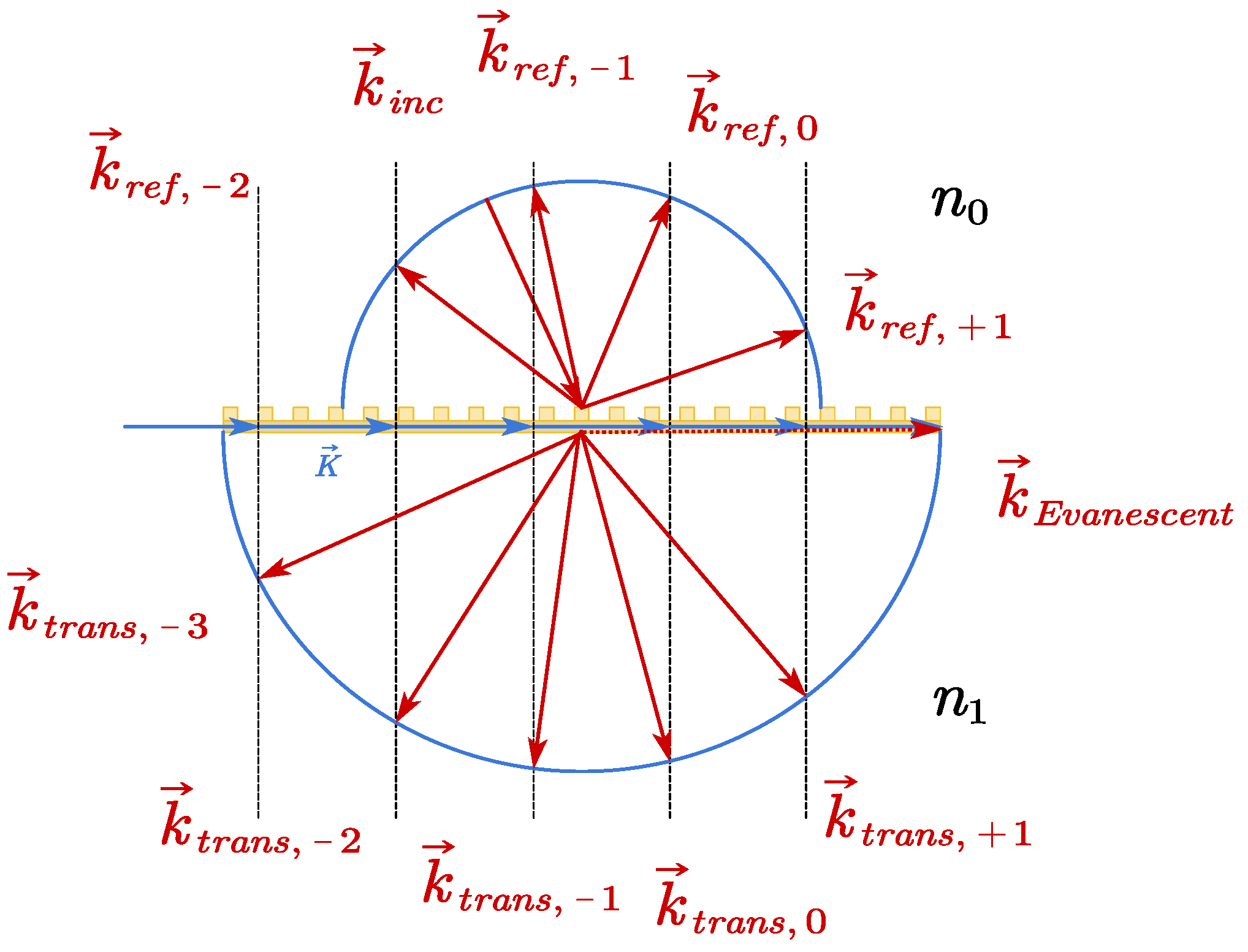
The endpoint of the transmitted wave vector must fall on the semi-circular arc that has been drawn. As shown in Figure 1, for a one-dimensional grating with normal incidence of the k-vector, the tracing process of the light ray can be described as follows:
- The incident wave vector determined by the wavelength and direction of the incident light is as in Figure 1.
- A semicircle of radius and is drawn, with the intersection point between and the plane of the grating as the center, as shown by the blue semicircles in Figure 1.
- Based on symmetry, the zero-order reflection wavevector is drawn, starting from the incident wavevector’s intersection point. A dotted line is drawn passing through the point of intersection between and the blue semicircle, perpendicular to the plane of the grating. The point at which this dotted line intersects the grating plane is determined. This intersection point is used as a base point to divide the grating plane into sections of length . Dotted lines are drawn perpendicular to the grating plane through each section’s dividing point.
- The dotted line intersects with the reflection and transmission side semicircles at the diffracted wavevectors , and , respectively, with the starting point at . However, the level at which the intersection point with the dotted line on the semicircle is located cannot be identified, which corresponds to the evanescent wave vector in Figure 1. The dotted line and semicircle on the reflection side and transmission side are diffractive wavevectors , and , whose starting point is the starting point of . The order where the intersection point with the dotted line cannot be found on the semicircle is the evanescent order, which is represented by the wave vector in Figure 1.
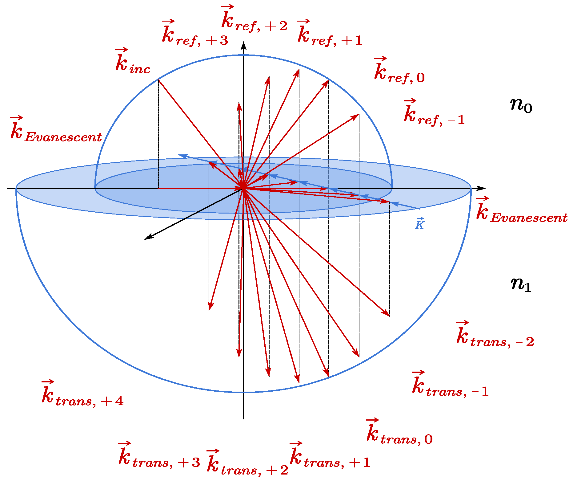
When the incident wavevector and the grating are not in the same plane, the diffraction of the grating is referred to as “conical diffraction” [22,23,24]. In this case, using the circular diagram of incident wavevector k shown in Figure 1 is no longer convenient to describe the deviation of light caused by the grating. Therefore, a spherical diagram of wavevector k is used to describe the deviation of light caused by the grating under oblique incidence. The tracing process of the oblique incidence with a one-dimensional grating follows the same procedure as that for normal incidence, except that the grating vector and the incident wavevector are not in the same plane. In the same manner, a spherical diagram of the incident wavevector is plotted to describe the deviation of light caused by the grating, as shown in Figure 2.
According to the spherical diagram of wavevector k, the curve formed by the reflection order – is exactly a half-cone, and the curve formed by the transmission order – is also a half-cone. Due to the difference in refractive index between the transmission and reflection regions, the radius of the half-cone is different in each case. Combining the cases of normal incidence and oblique incidence, in a one-dimensional grating, due to the spatial invariance of the planar interface, the tangential component of the diffracted wavevector differs from the tangential component of the incident wavevector by an integer multiple of the tangential component of the grating vector of the modulation grating. The generalized one-dimensional grating diffraction equation for volume holographic gratings can be written as:
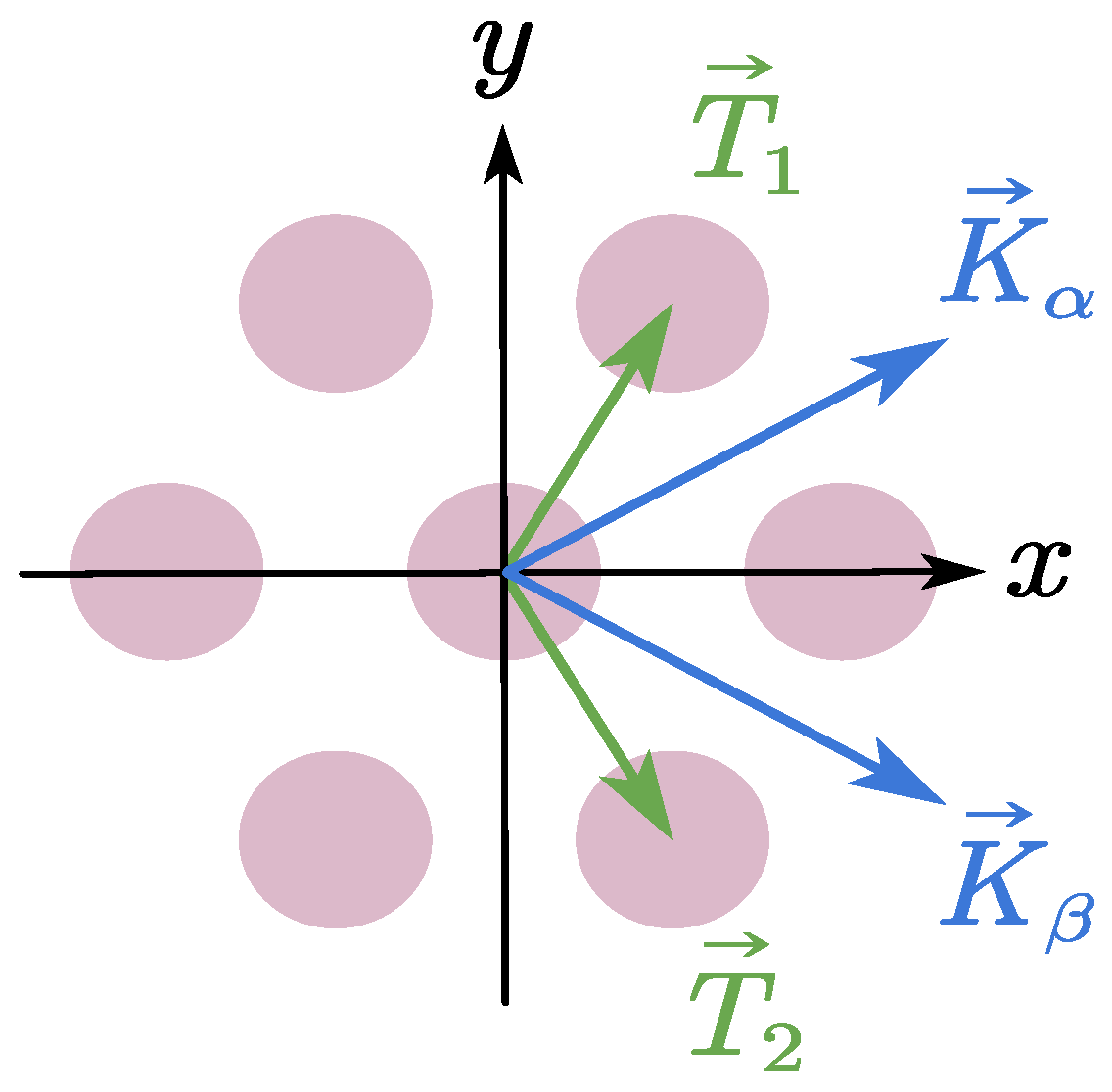
represents the angle between the grating vector and the normal to the planar interface. The addition of one degree of freedom in the two-dimensional grating results in an increase in the number of grating vectors from one to two, necessary to describe the far-field diffraction behavior of the grating.
As depicted in Figure 3, and represent the primitive translation vectors of a two-dimensional hexagonal lattice, and their corresponding primitive reciprocal lattice vectors and can be obtained through the reciprocal lattice relation. When the diffraction grating exhibits two-dimensional periodicity, its grating vectors are essentially the primitive reciprocal lattice vectors of its periodic lattice in reciprocal space. There exists a relationship among the tangential component of the diffracted wavevector, the tangential component of the primitive reciprocal lattice vector in reciprocal space, and the tangential component of the incident wavevector in the plane interface.
and represent the primitive translation vectors of the two-dimensional periodic lattice of the diffracting grating, as follows:
2.2. Diffraction Waveguide System Modeling
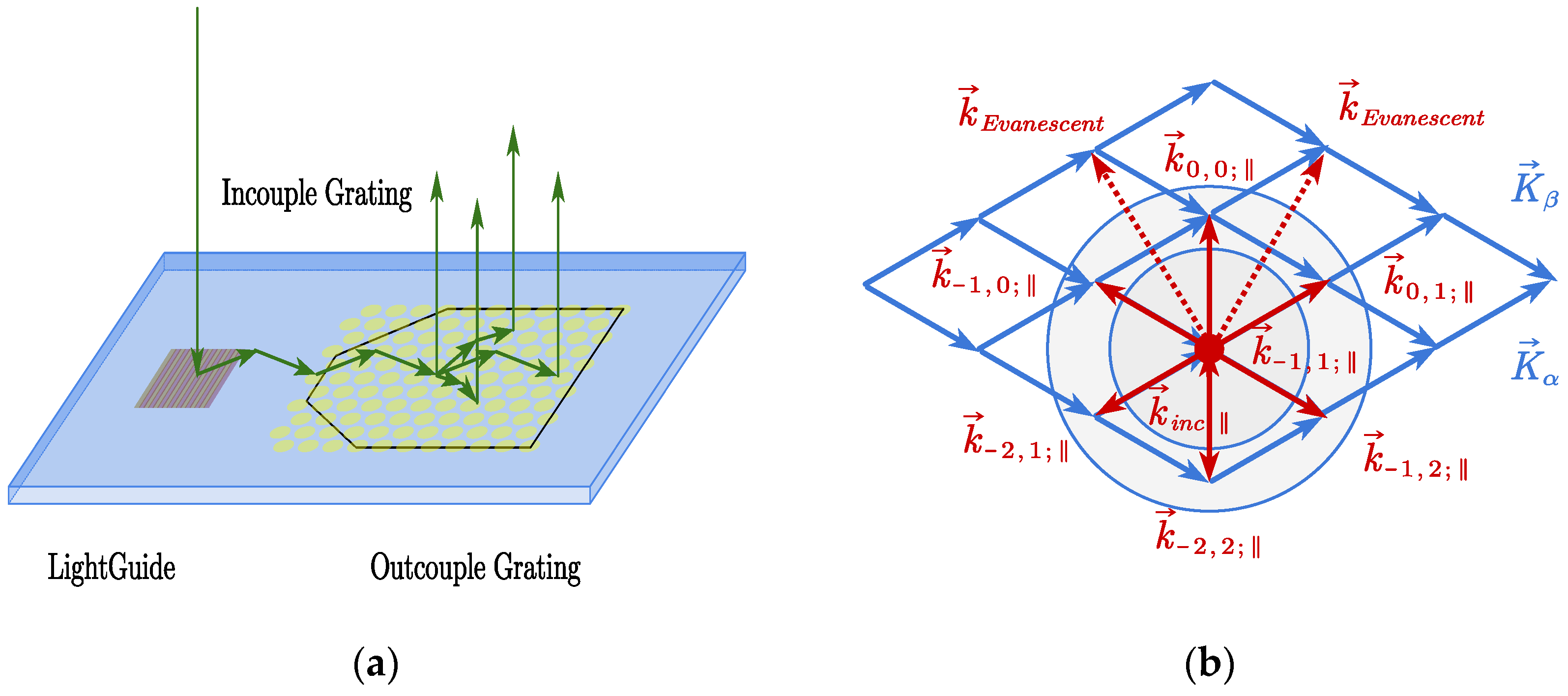
The diffractive waveguide and its coupler are the most critical components in diffractive waveguide systems capable of achieving 2D-EPE. To make the diffractive waveguide system more compact and lightweight, we used a VHG as the input coupler and a 2D holographic grating as the output coupler to achieve 2D-EPE. The grating layout in these two regions effectively reduced the volume of the optical system, providing a better user experience for wearing and use. In the modeling process, a traditional reflecting volume holographic grating was used as the input coupler due to its wider angular bandwidth than a transmitting volume holographic grating, which allows for a larger field of view and higher energy utilization, as it only has one diffraction order. In this work, the designed 2D holographic grating was used as the output coupler.
In optical simulation software such as Zemax OpticStudio, tracing of light rays requires attention to their deflection direction and energy distribution, which is achieved through phase modulation of the incident light according to the diffraction plane [25]. This is expressed as ΔLout = ΔLin + , where ΔLout and ΔLin are the optical path differences at the output and input:
and are the refractive indices of the incident and exit media, respectively. and are the direction cosines of the incident and exit light in the x direction, while and are the direction cosines of the incident and exit light in the y direction. and are the moduli of the initial basic displacement vectors of the two-dimensional periodic structure; and are the direction cosines of the initial basic displacement vector in the x and y directions, respectively. and are the orders of the two-dimensional diffraction.
The Zemax OpticStudio nonsequential mode enables free definition of optical surfaces by custom objects with DLL functions. In order to realize ray tracing of 2D gratings, a DLL is developed based on the ray tracing k-vector circle diagram model proposed in Section 2.1 and the analysis of 2D grating ray tracing in Equation (5), which has the function of 2D ray tracing and the ability to adjust the primitive lattice slip vector, thus allowing the simulation of all types of 2D gratings. This DLL function can still predefine its own diffraction efficiency and use the diffraction efficiency hyperparameters as optimization variables to participate in the optimization of optical uniformity and optical energy utilization.
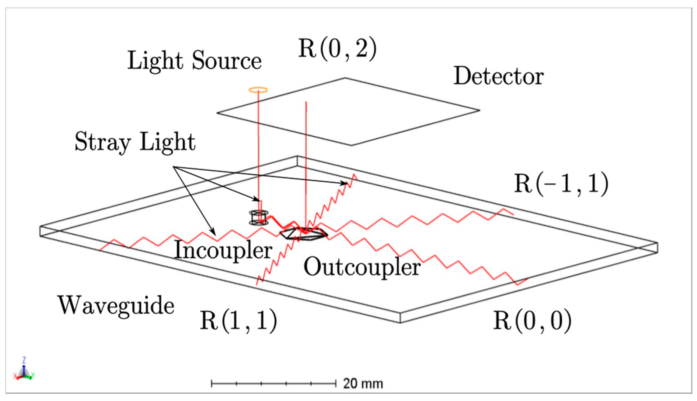
As shown in Figure 4, an out-coupler with a custom DLL as a spectral function is used as a coupled-out device for the diffractive waveguide system. Its (0,2) order reflection is injected into the human eye as the coupled-out light, while the diffracted light of the (0,0), (−1,1), and (1,1) order expand the image to the left, right, and front directions, respectively. The stray light appears because the (0,0) order coupled out light passes through the upper surface of the flat waveguide and is generated due to the reflection of the interface. In order to improve the light efficiency of the whole system and the imaging quality, the upper surface of the flat waveguide needs to be coated with an antireflection. When designing a diffractive waveguide coupling device using a custom DLL, the diffraction order and diffraction efficiency can be determined first based on the optical index. This diffraction efficiency is then obtained by optimizing the process parameters through a third-party algorithm, and the flexibility of the third-party algorithm is used to further enhance the development efficiency.
2.3. Ray Tracing Optimization Design
A 2D grating array is used as a diffraction waveguide system for coupled gratings, and 2,000,000 rays need to be traced to ensure the accuracy of the results. In order to improve the efficiency of ray tracing and to ensure the smooth iteration of the objective function, the ray tracing is optimized.
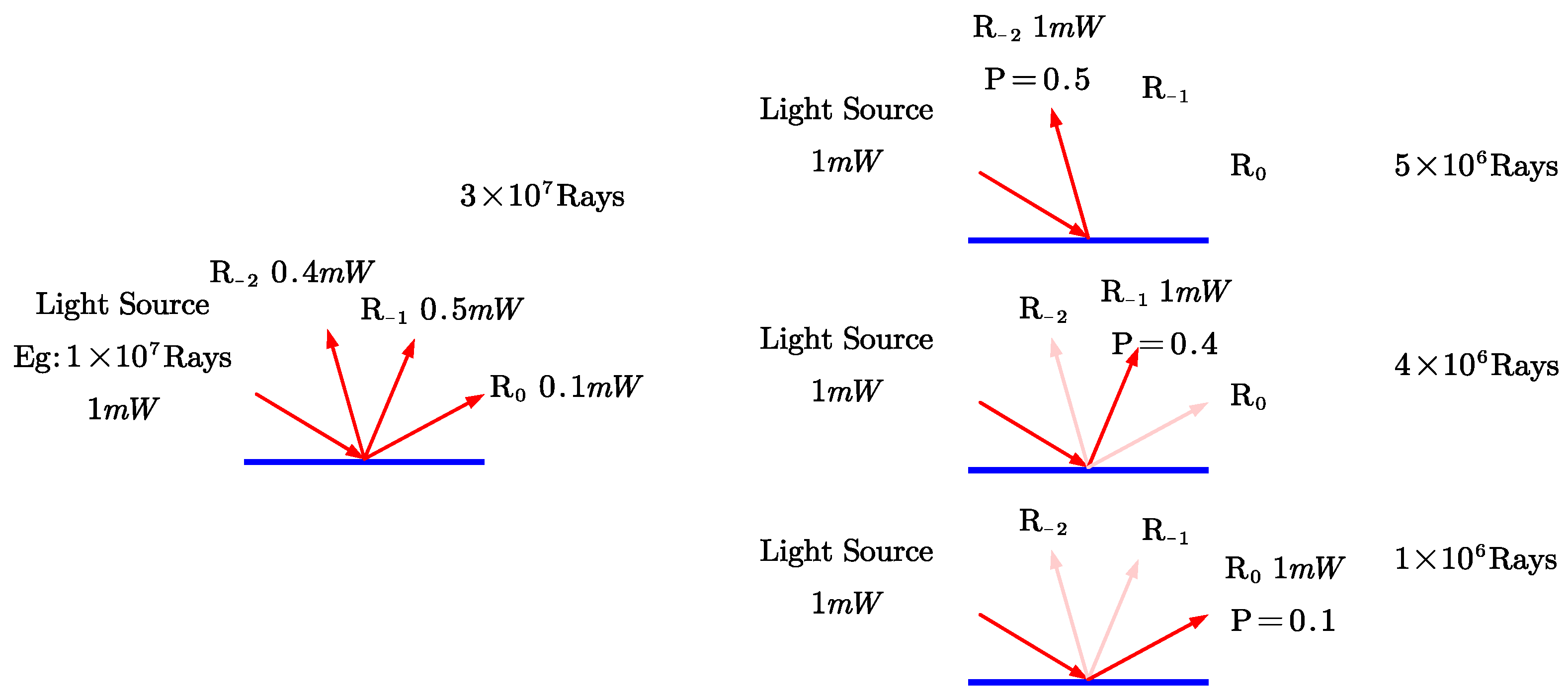
The multi-order diffraction behavior of a 2D-EPE coupler is simulated by Zemax OpticStudio. The relative energy carried by each diffraction order of a 2D grating is obtained from the diffraction efficiency calculated by RCWA. For a grating surface with three diffraction orders, a light beam carrying 10 mW of energy is incident with three diffraction orders of 1 mW, 4 mW and 5 mW, respectively. The function of probabilistic splitting is applied in the custom object and when a light carrying 10 mW of power is incident on the 2D-EPE coupler, the energy efficiency distribution of the diffraction order is used to determine the probability of tracing the secondary according to the diffraction order. As shown in Figure 5, the probabilities of occurrence of 1, 4, and 5 mW are 0.1, 0.4, and 0.5, respectively; each incident ray striking the 2D grating surface will trace only one outgoing ray with the same power of 10 mw as the incident ray but with different angles and according to the probabilities of 0.1, 0.4 and 0.5.
To ensure the accuracy of the image simulation, Zemax OpticStudio is used to trace rays in one iteration cycle. The Monte Carlo method is used to simulate the case of multi-order grating diffraction, using only uniformly distributed random samples. The implementation is as follows: first, a random number seed is defined, and a uniformly distributed random number S in the range of 0 to 1 is generated using this seed. Then, a state vector is defined based on the diffraction efficiency, which can determine the state of the random number and, thus, the probability of tracing the ray. Following the previous example, if the diffraction efficiencies of three diffraction orders are 0.1, 0.4, and 0.5, respectively, then the generated state vector is L = [0, 0.1, 0.5, 1.0]. Then, the random number S is compared with the state vector L: if S < L[1] and S > L[0], the traced ray will be the diffraction order with efficiency 0.1; if S < L[2] and S > L[1], the traced ray will be the diffraction order with efficiency 0.4; if S < L[3] and S > L[2], the traced ray will be the diffraction order with efficiency 0.5.
2.4. Waveguide Coupler Device Fabrication
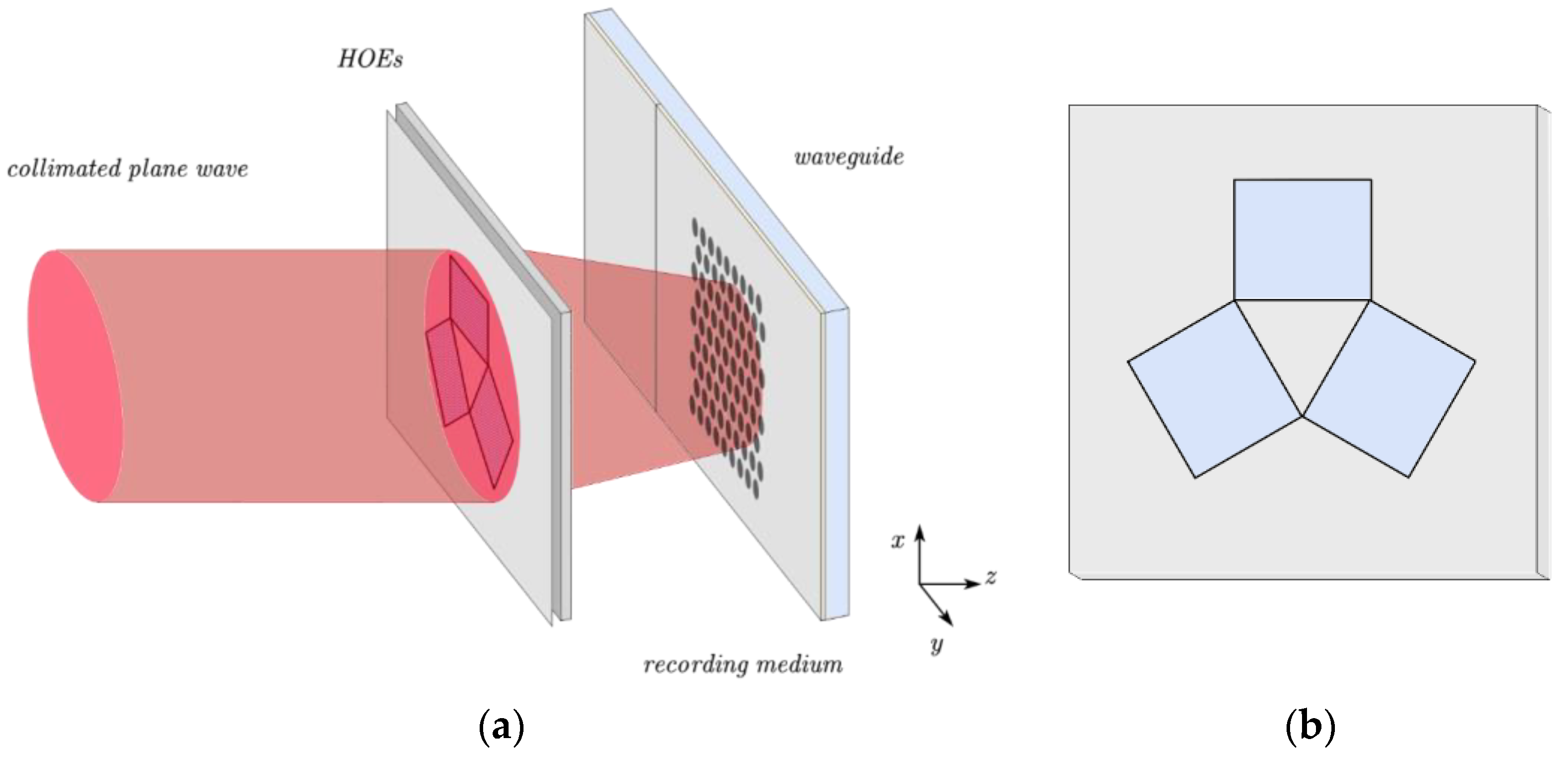
We propose a holographic lithography apparatus composed of holographic optical elements (HOEs) and a method for fabricating HOEs. We also simulate the refractive index spatial distribution of a 2D coupler prepared using a photosensitive resist as the recording material. The 2D holographic grating is fabricated using the holographic lithography apparatus shown in Figure 6a; a collimated and expanded plane wave is incident on the diffraction screen with HOEs, and the diffracted light intensity forms a periodic spatial distribution in the optical recording medium on a planar waveguide, inducing a spatial distribution of refractive index. The relative positioning and arrangement of HOEs, as shown in the Figure 6, with the square region representing the HOE and other regions made of purely absorbing materials, are designed to avoid the influence of stray light.
According to the theoretical analysis of 2D hexagonal photonic crystals made using HOEs, the lattice constants:
refers to the wavelength of the light source used in vacuum to fabricate the 2D holographic grating and represents the first-order diffraction angle of the light passing through a single HOE. denotes the refractive index of the ordinary waveguide substrate, the value of which is 1.723. The light source for the display is a He–Ne laser with a wavelength of 632.8 nm, while a He–Cd laser with a wavelength of 442 nm is used to fabricate the 2D holographic grating on the photosensitive resist. According to equation , the required first-order diffraction angle for the HOE is obtained as .
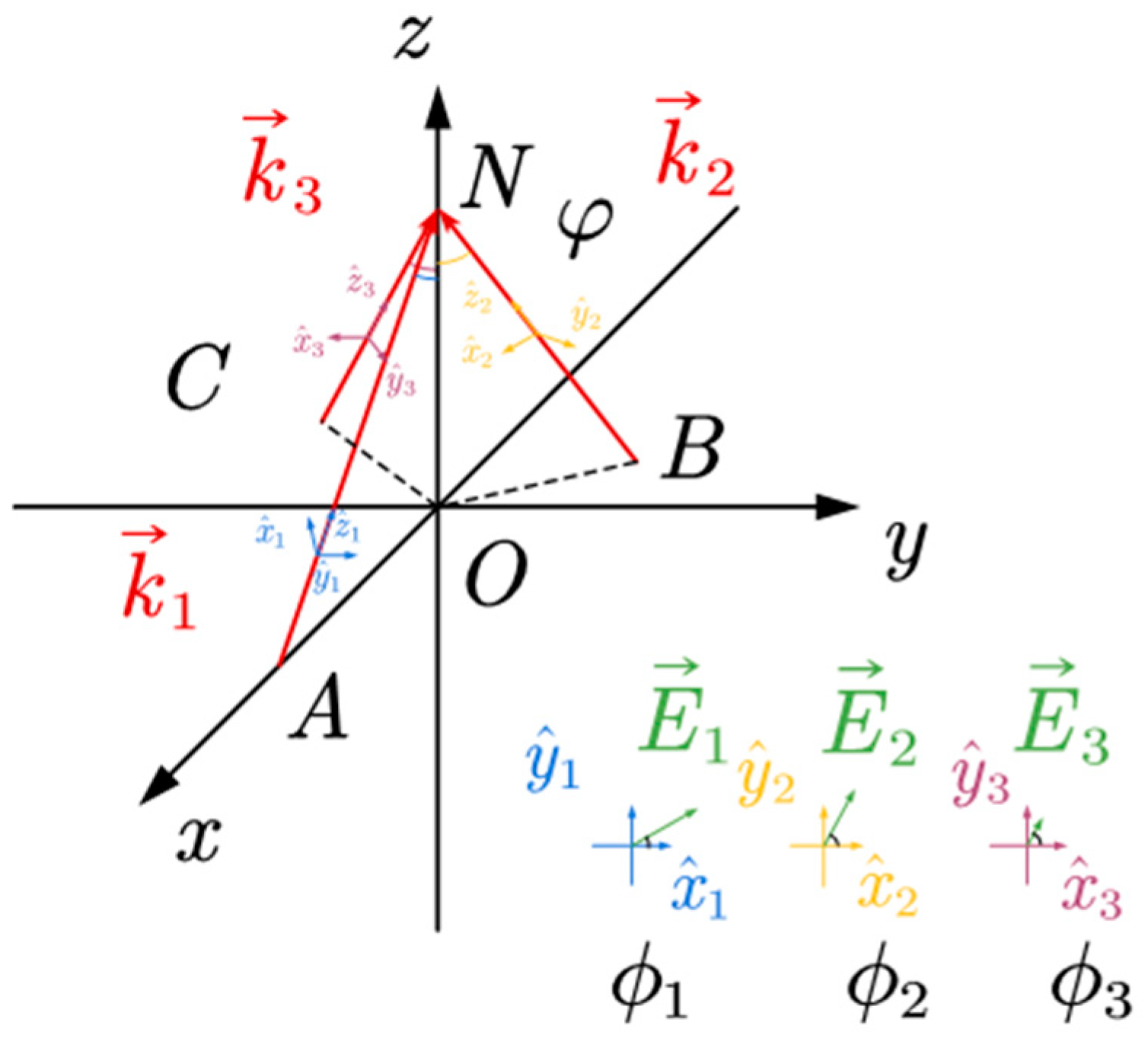
The fabrication of the two-dimensional grating is accomplished using holographic techniques. The first step involves interference, and analyzing the intensity of the interference light is beneficial for accurately guiding the fabrication experiment. Figure 7 represents the three-beam interference; the wave vectors of the three-beam plane wave are:
The distribution of optical intensity of the recording medium is:
The angle between the three planar waves and the surface normal is denoted as , which is also the primary diffraction angle of HOEs. As shown in Figure 7, the amplitudes of the three planar waves are , and , and their polarization angles observed in the relative co-ordinate system are , and , respectively.
Therefore, the components of the three planar waves in the cartesian co-ordinate system are given by:
By substituting Formula (9)–(11) into Formula (8), the interference field intensity distribution of the three plane waves can be obtained as follows:
Based on the light intensity distribution analyzed in Equations (7)–(12), the 2D holographic grating obtained by the holographic lithography method is completely described in combination with the photoresist model proposed in this section. The positive photoresist is selected as the recording material, and the part that absorbs photons is dissolved away after development, and the part that does not absorb photons is retained due to the slow corrosion rate; the thickness of the photoresist can be expressed as , where the corrosion depth of the positive photoresist is determined by two parts: one is the photoresist corrosion rate of the absorbed photon part and the other is the corrosion velocity of the unabsorbed photon part . Substituting both velocities into the above equation ; since , the equation can be reduced to . ; therefore, the refractive index distribution of the recorded material can be expressed as is the photoresist thickness, is the original refractive index of the photoresist, and for the positive photoresist selected in this work, the refractive index .
The refractive index distribution of photoresist is not only related to the periodic distribution of light intensity but also closely related to the treatment process of photoresist. Therefore, for the 2D holographic grating prepared by using photoresist, the influencing factors of the spatial distribution of refractive index n(x, y, z) are A1, A2, A3, ϕ1, ϕ2, ϕ3, Td, t, and T. The 2D holographic grating with the desired spatial distribution can be prepared by reasonably adjusting the light intensity ratio, polarization state, exposure time, and development time of the three beams involved in the interference.
2.5. Inverse Design of Electromagnetic Structures
We have developed a program, Holo-RCWA, based on the traditional RCWA algorithm process. The program exhibits excellent robustness and efficiency in solving the electromagnetic response of holographic recording materials using photoresist. Additionally, it overcomes the weakness of the slow convergence speed of the traditional RCWA algorithm when TM-polarized incidence is applied.
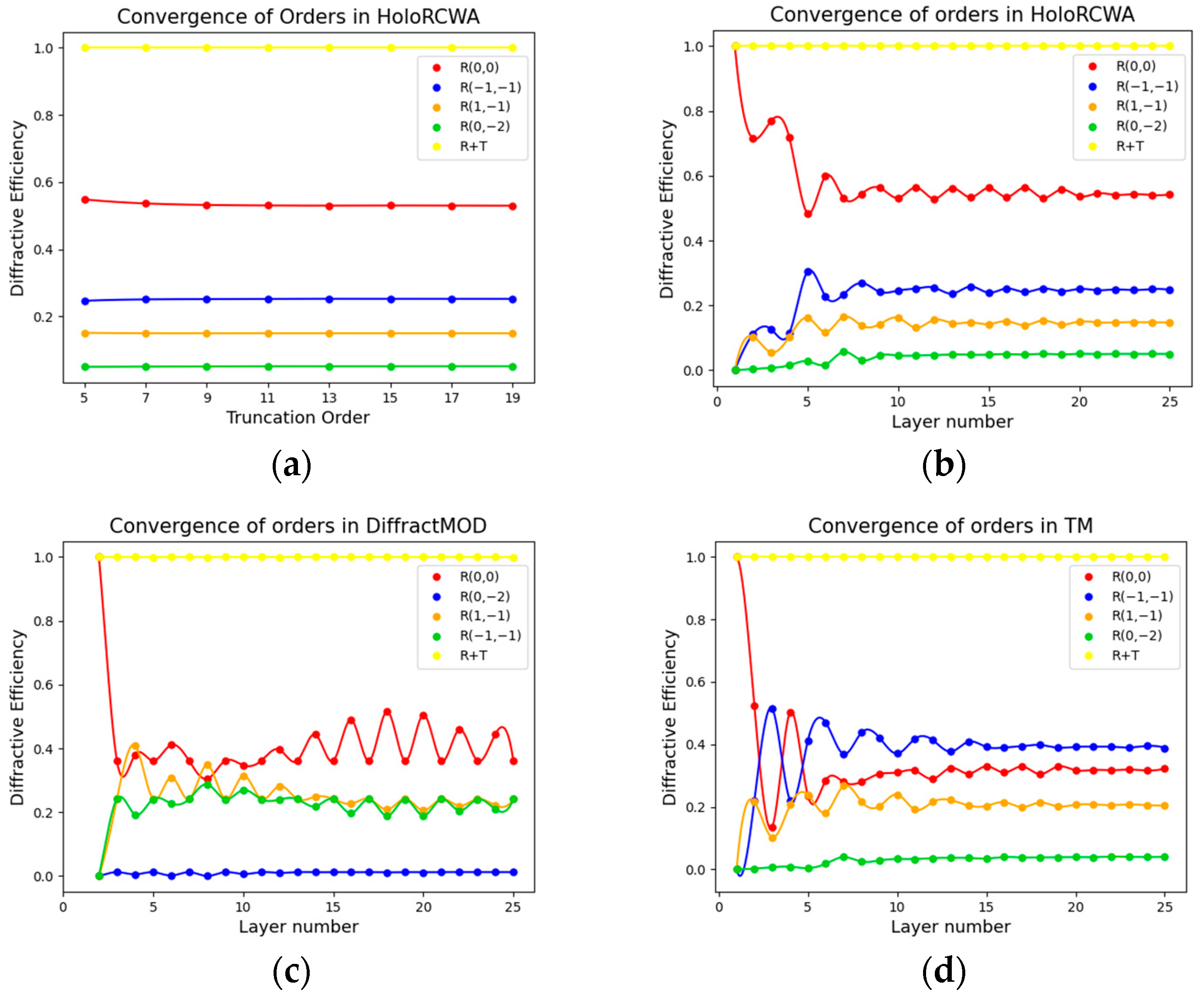
As shown in Figure 8a, when using the 2D holographic grating prepared using photoresist as holographic recording materials, which was calculated by the Holo-RCWA program developed, only five Fourier harmonics are required in each direction (x and y) to achieve convergence. This is because the 2D holographic grating produced by the photoresist preparation method does not have a refractive index jump like rectangular gratings produced by methods such as nanoimprinting, thus requiring fewer Fourier harmonics to converge the calculation. The 2D holographic grating model of the photoresist established in Section 2.4 is compared based on z-axis co-ordinates with the remaining height of the etched photoresist. If the z-axis co-ordinate is greater than the remaining height of the photoresist at that point, the refractive index is set to air; if the z-axis co-ordinate is less than or equal to the remaining height of the photoresist at that point, the refractive index is set to the refractive index of the photoresist. The modeling of the photoresist holographic grating is in line with the calculation process of the RCWA algorithm.
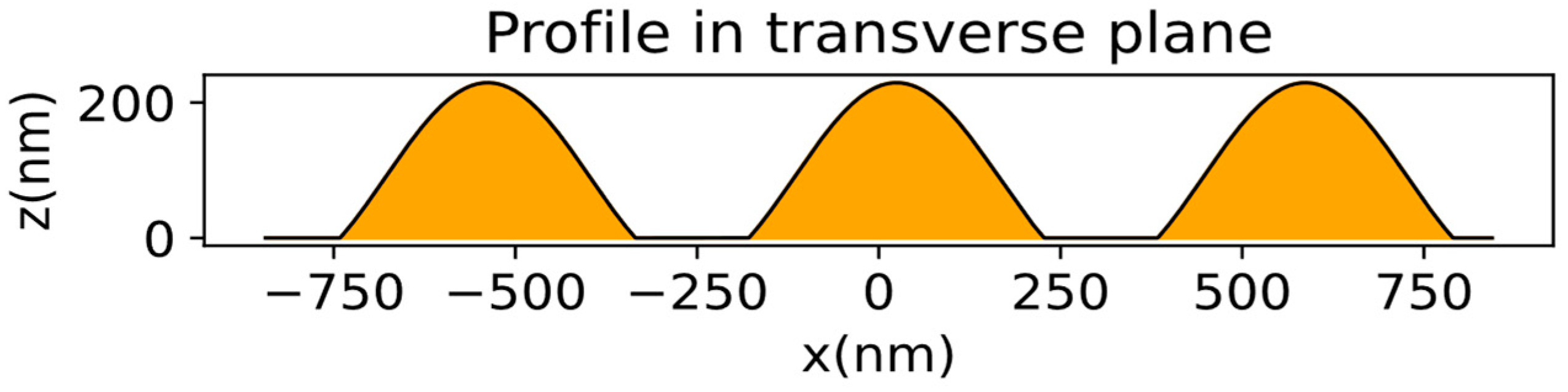
As shown in Figure 9, the x-z profile of the 2D holographic grating is characterized by periodic modulation. When RCWA calculates the electromagnetic waves passing through the structure, it divides the structure by a plane perpendicular to the z axis. Holo-RCWA adopted an even division strategy. As shown in Figure 8b, when Holo-RCWA calculates 2D holographic gratings prepared by photoresist, the calculation results converge quickly with the number of layers; when the number of layers is 7, the calculation results tend to be stable, while, when the number of layers is 20, the calculation results remain stable. At the same time, the total diffraction efficiency is always conserved. These two points together explain the reliability of the calculation results. Figure 8c shows the results of commercial software calculations. When the number of layers is divided into 25 layers, the calculation results still do not show the trend of convergence. Compared with Figure 8b,c, when Holo-RCWA solves the 2D holographic grating proposed in this work, the convergence rate of the calculated results is significantly faster than that of commercial software, and the results are stable and have excellent robustness. Figure 8d shows the calculation results of Holo-RCWA at TM mode incidence. When the number of divided layers is less than five layers, the calculation results show great volatility, which is consistent with the performance of the traditional RCWA algorithm in the same scenario. However, when the number of layers is greater than 10, the calculation results jump out of the oscillation period quickly and remain stable with the increase in the number of layers. As shown in Figure 8, the Holo-RCWA program proposed in this paper has excellent performance, and its ability to solve complex problems is significantly enhanced compared with the traditional RCWA program.
3. Results
3.1. 2D-EPE Diffractive Waveguide Architecture
Figure 10a shows the basic architecture of 2D-EPE, where a volume holographic grating (VHG) is used for coupling. The angle between the central field ray of the propagated image in the waveguide and the interface normal is 60°. The output coupling grating is a 2D grating, where the incident light enters the reflective 2D grating structure with a polar angle of 60° and an azimuth angle of 90°. The (0,0) diffraction order continues to propagate by total internal reflection (TIR) after interacting with the 2D grating structure, while the (0,1) diffraction order reflects with a polar angle of 60° and an azimuth angle of 30°, and the (−1,0) diffraction order reflects with a polar angle of 60° and an azimuth angle of 150°. The (−1,1) diffraction order directly exits vertically as the center field egress ray. The (0,0) order ray interacts with the 2D grating structure after TIR with the waveguide upper surface, repeating the aforementioned process. The (0,1) and (−1,0) order diffracted rays repeat the same process in their respective local co-ordinates. The parallel component of the k-vector of the replicated egress rays is shown in Figure 10b.
The design of the diffractive waveguide coupled grating period is as follows: when the tangential component of the k-vector of the (−1,1) order diffracted ray is equal to zero, central field vertical emission can be achieved. The grating vector of the 2D grating is given by:
Therefore, the required lattice constant of the 2D holographic grating is , where n is the refractive index of the waveguide medium and is the wavelength of the display’s light source in vacuum. The grating vectors and of 2D grating are the primitive translation vectors of the 2D periodic lattice shown in Figure 3a. Based on the center field EPE, the initial architecture of the diffractive waveguide using a 2D grating as the exit pupil coupling device has been designed.
3.2. 2D-EPE Simulation and Optimization Results
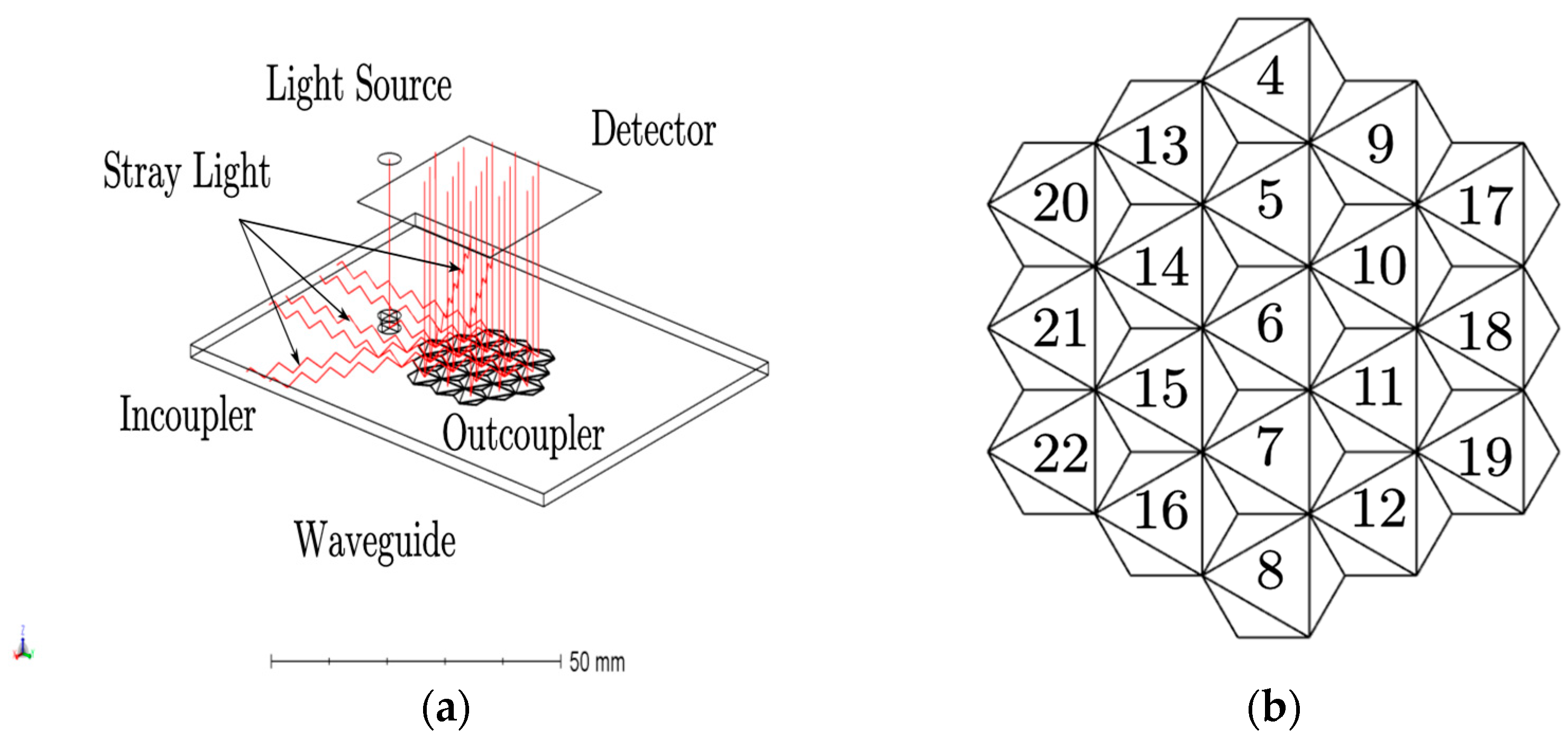
The optical parameters of HMD, such as FOV, chromatic aberration, color uniformity, brightness uniformity, and light efficiency, need to be considered during the design phase. Sufficiently flexible parameter settings can help the evaluation function quickly escape from local minima. The optimization variables are determined based on the shape and microstructure of the input and output coupling gratings, while the evaluation function is determined according to the specified targets. Iterative optimization of the variables is conducted using software like Zemax OpticStudio [26,27]. In this paper, a diffractive waveguide system was simulated, using a volume holographic grating as the input coupling grating and a 2D grating as the output coupling grating, as shown in Figure 11a. By partitioning the output coupling grating, the multi-order diffraction efficiency of different sub-regions was set as the optimization variable while keeping the shape of the input and output coupling gratings unchanged.
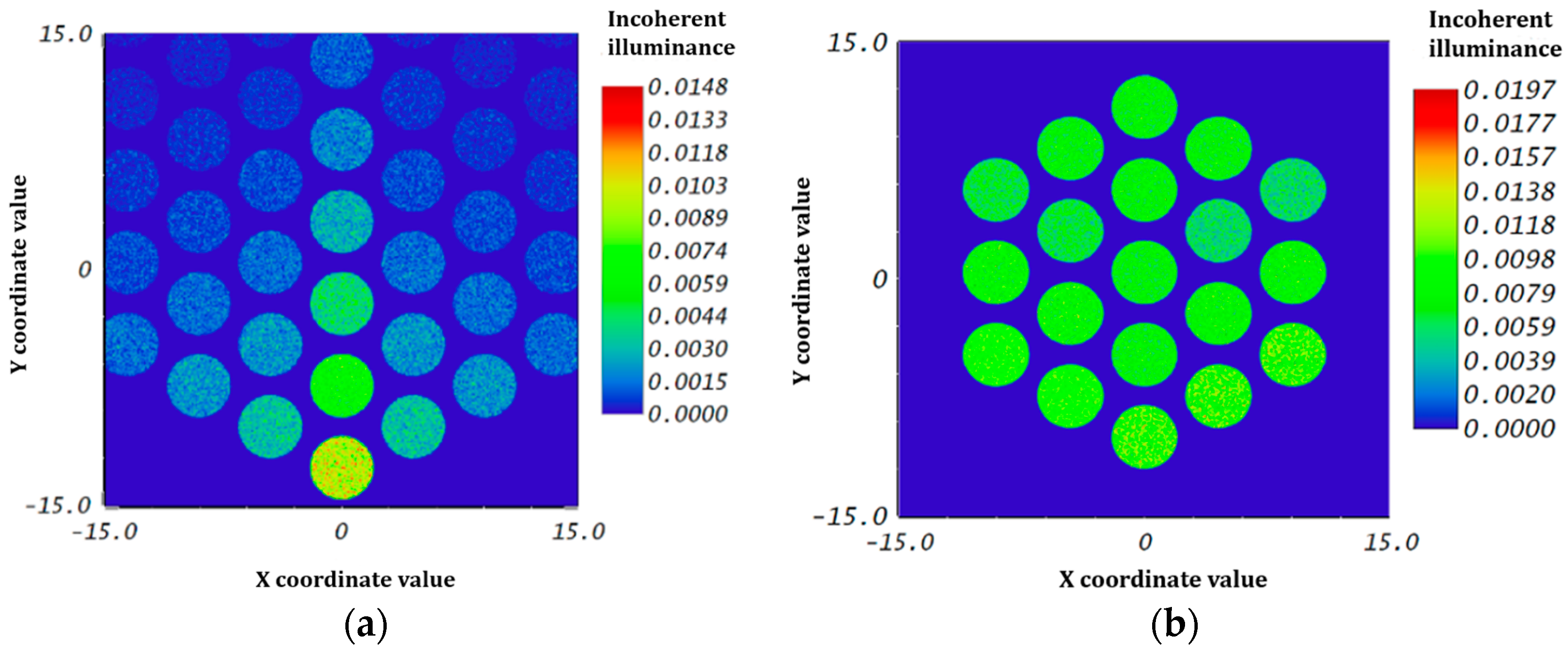
The output coupling grating region is shown in Figure 11b. The output coupling grating was partitioned into hexagonal sub-regions. Each hexagonal 2D grating has a uniform periodicity but a different surface profile, causing the same angle of deflection for incident light rays but different diffraction efficiency distributions, which are collectively combined to form a honeycomb-like array of the output coupling grating. Through software simulations, we established 22 optimization variables and employed brightness uniformity and light energy utilization evaluation as the objective functions for our optimization process. The (−1,1), (1,1), (0,0), and (0,2) diffraction orders of regions 4, 5, 6, 7, and 8, as well as the corresponding diffraction orders of other regions, were set as optimization variables for further optimization. As shown in Figure 12, when the output coupling grating was not partitioned, the standard deviation of the detector grid illuminance data was 0.00189, while the light efficiency was 0.73%. When the output coupling grating was partitioned, the standard deviation of the illuminance data increased to 0.00274 but the light efficiency increased to 1.9%. This resulted in a significant increase in display brightness with high uniformity maintained. Compared to the nonoptimized model, the light efficiency was significantly improved.
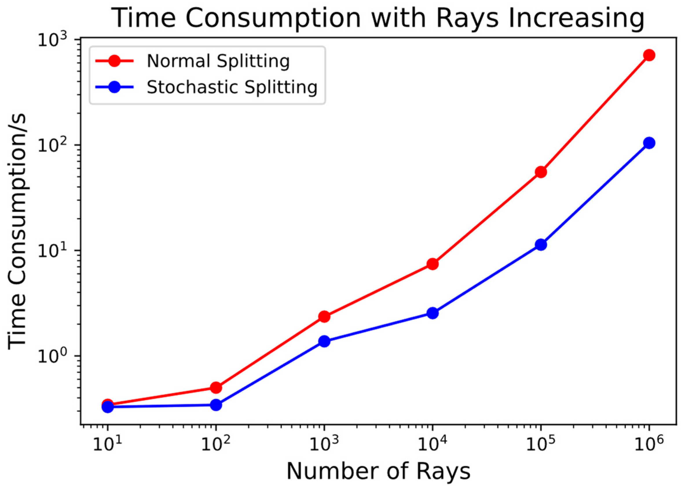
The experimental results of tracing the 2D grating DLL diffraction function optimized using Monte Carlo ray tracing are shown in Figure 13. After adopting probabilistic splitting, the simulation time was reduced from 11.852 min to 1.744 min per iteration. The time difference in ray tracing consumption increases as the number of traced rays increases, with typically millions of rays required for nonsequential simulation of optical systems. As the complexity of the optical system increases, such as in diffractive waveguides where multiple traces of the same object are required, the superiority of the probabilistic splitting DLL optimized by Monte Carlo ray tracing in this study will gradually emerge.
3.3. Simulation Results of Photoresist
The refractive index of photoresist is influenced by the periodic distribution of light intensity and the treatment process of photoresist. The factors affecting the spatial distribution of refractive index of the 2D holographic grating prepared by using photoresist are . The desired spatial distribution of the 2D holographic grating is prepared by reasonably adjusting the light intensity ratio, polarization state, exposure time, and development time of the three beams involved in the interference.
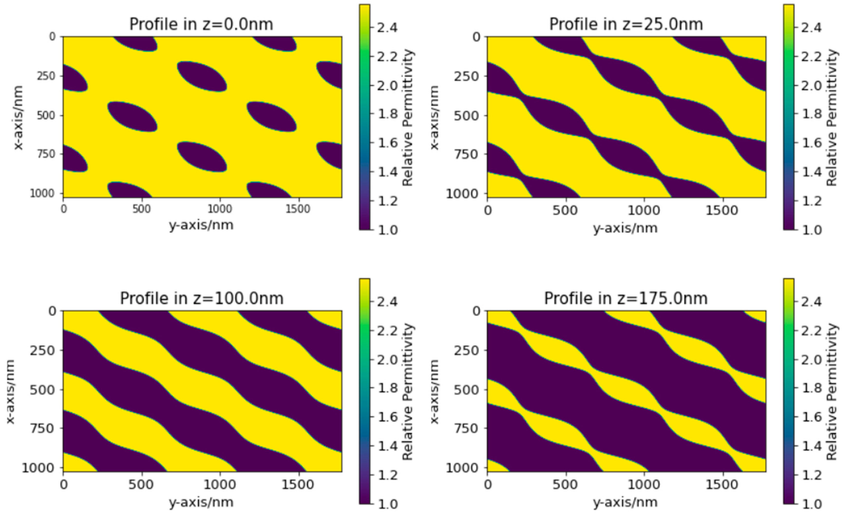
The spatial distribution of the relative dielectric constant of the photoresist, representing the XY profile, is illustrated in Figure 14 for the given parameters as presented in Table 1. Each image in Figure 14 corresponds to the topographical features of a 2D holographic grating composed of four periods. The yellow region denotes the relative dielectric constant of the photoresist, while the purple–black region indicates the portion of the photoresist that has been selectively etched by the developer solution, resulting in a relative dielectric constant of 1. By precisely controlling the development time and the intensity of light, it is feasible to achieve full etching of the photoresist, leading to the emergence of a region with a relative dielectric constant of 1 at z = 0.0 nm.
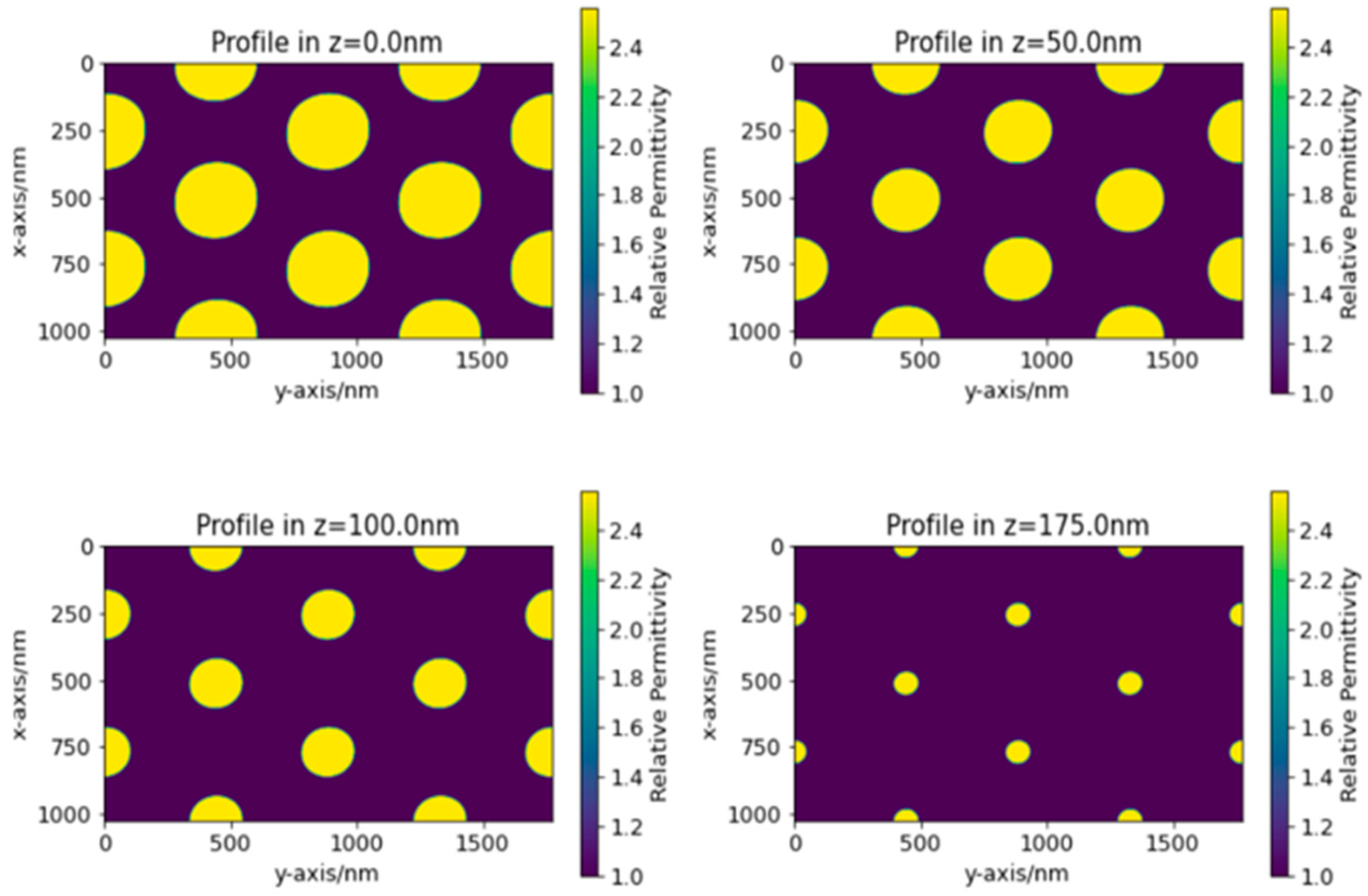
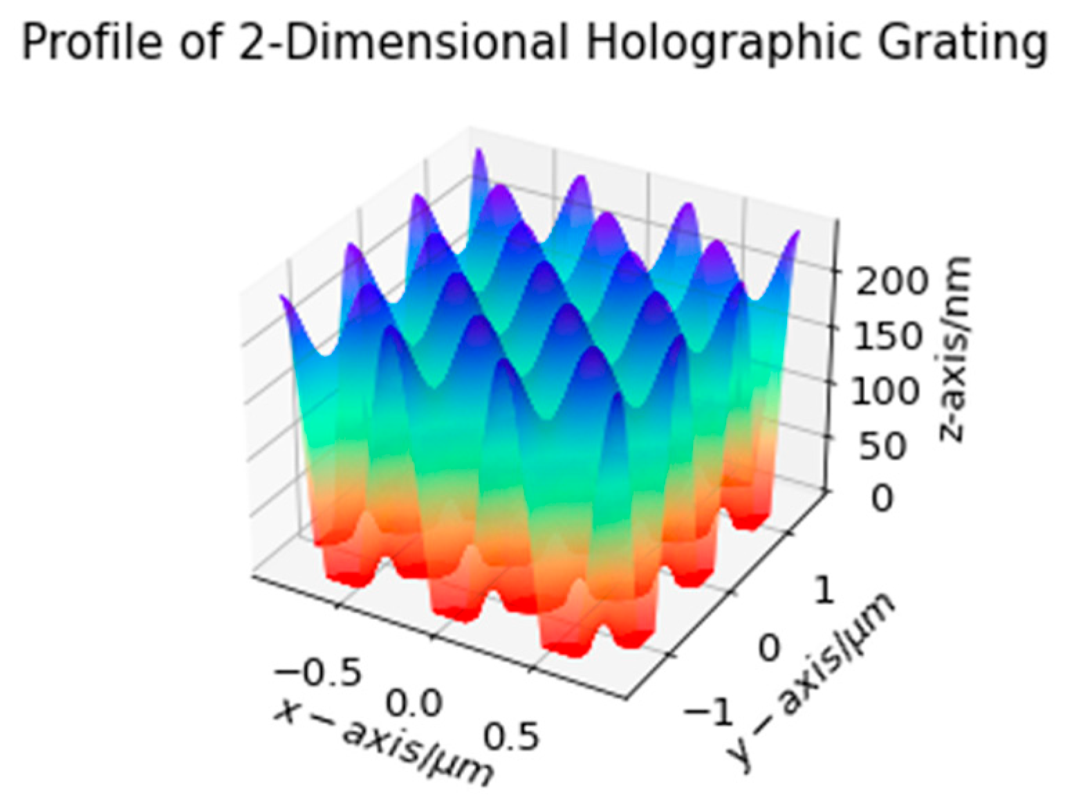
By appropriately adjusting the polarization states of three light beams, the optical morphology of a 2D holographic grating can be effectively controlled. When ϕ1 = 10°, ϕ2 = 180°, ϕ3 = 10°, and the development time Td = 40 s, along with the other parameters as listed in Table 1, the spatial distribution of the relative dielectric constant of the photoresist is shown in Figure 15. By varying the polarization states, there is a noticeable modification in the profile of the 2D holographic grating. Therefore, the optical properties of 2D holographic grating can be effectively adjusted. As shown in Figure 16, a periodic structure with high and low undulations is obtained through holographic lithography of the photoresist. Its diffraction characteristics are determined by the Raman–Nath Law [28,29]. By controlling the parameters listed in Table 1, the morphology of the 2D grating can be flexibly adjusted, thus altering the diffraction efficiency distribution of the grating. Therefore, the required parameters can be inverse designed by using the optimized diffraction efficiency hyperparameters obtained in Section 3.2, providing guidance for the preparation of the experiment.
3.4. Multi-Objective Optimization Results
In order to make the exit pupil of the diffractive waveguide expand uniformly and, at the same time, ensure a good utilization rate of light energy, we use Holo-RCWA combined with the evolutionary algorithm NSGA-II to carry out inverse design of the grating preparation process. The inverse design goal of the process parameters in Table 1 is to make the diffraction efficiency distribution of the outcoupling grating array as shown in Figure 12b.
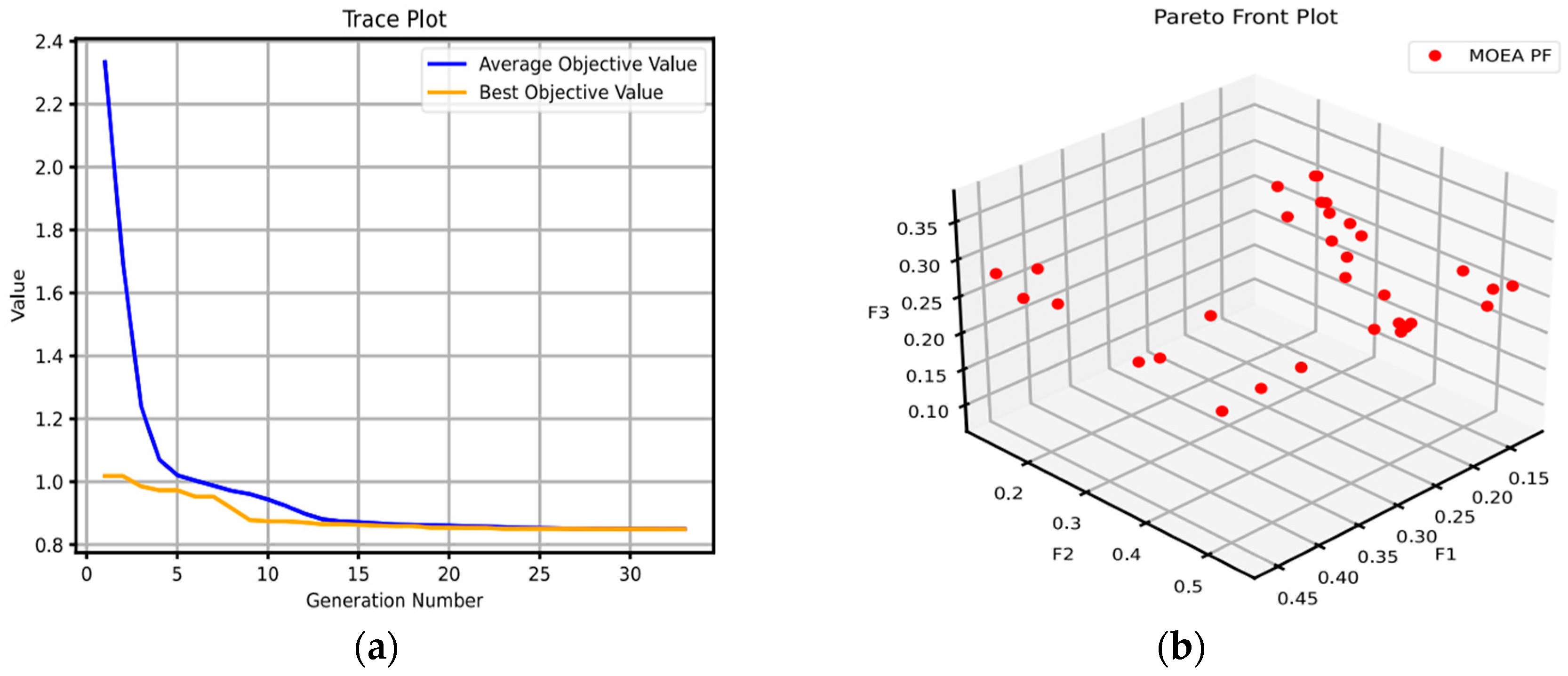
Figure 17a shows the single-objective optimization results of direct weighted summation of the evaluation function when the incident excitation of the 2D diffraction grating is set as TE wave, TM wave, and plane wave whose polarization direction is on the bisector of TE and TM polarization direction angles. The maximum number of evolution generations is 50, and the number of individuals in the population is 50. When the evolutionary generation reaches 15 generations, the individual that best meets the objective function has appeared, and the average performance of the population becomes better as the evolutionary generation increases. However, no method has been found to prove that the solution obtained by the weighted sum satisfies the three polarization states and is the closest to the inverse design goal. Therefore, it is necessary to establish evaluation functions for different polarization states at the same time and use a multi-objective optimization algorithm for inverse design. Figure 17b shows the multi-objective nondominated solution set when using NSGA-II. The maximum number of evolution generations is 100, and the number of individuals in the population is 50. The figure shows 32 Pareto solutions, and the co-ordinate value of each Pareto solution in the solution space represents the objective function value when different polarization states are incident, and each point represents a set of experimental parameters. Therefore, according to the optimization results of single-objective and multi-objective optimization, the corresponding experimental parameters can be further determined and a 2D grating conforming to the predetermined efficiency distribution can be prepared. Performing 19 inverse designs in parallel and adjusting the experimental parameters makes the holographic waveguide system with 19 sub-area out-coupling grating arrays meet the exit pupil illumination distribution as shown in Figure 12b.
In this section, the single-objective optimization takes 1 to 2 h, while the multi-objective optimization takes about 8 h. Compared with the optimization time of the traditional method of 2 to 3 days, the method proposed in this paper can, indeed, greatly shorten the development cycle. At the same time, genetic algorithms can naturally further improve optimization efficiency through parallel computing [30]. CUDA is a parallel computing platform and programing model developed by NVIDIA that allows developers to utilize NVIDIA’s GPUs for general-purpose parallel computing. The CUDA version of Holo-RCWA and NSGA-II predictably have the ability to further reduce the original optimization time from 8 h to shorter but, unfortunately, due to the lack of corresponding hardware conditions, this paper did not conduct specific comparative experiments.
4. Conclusions
In summary, we designed and studied a holographic waveguide system that focuses on 2D diffraction gratings and can realize dual-region 2D-EPE. The initial structure of the waveguide system was determined through the ray tracing model, and Zemax OpticStudio was used to model and simulate the diffractive waveguide system. The proposed honeycomb coupling grating array achieved optimization of the light energy utilization and brightness uniformity of the holographic waveguide. A custom DLL function was used to implement ray tracing of 2D gratings, and a probabilistic splitting function was added to the DLL to reduce the single simulation time from 11.853 min to 1.77 min. In order to obtain the preoptimized diffraction efficiency of DLL for exit pupil brightness uniformity and light energy utilization, reverse design was carried out using the preparation process parameters as optimization variables, and a highly adaptable electromagnetic calculation program Holo-RCWA was developed, which was combined with the multi-objective evolutionary algorithm NSGAII inverse design. Design process parameters that meet the diffraction efficiency distribution and shorten the optimization time of the entire system from 2 to 3 days to 10 h. The optimization results will further guide the development of subsequent experiments. This work further provides theoretical and practical support for the use of HVG in diffractive waveguide technology, providing new technological approaches and promising candidate materials for AR/VR applications.
Author Contributions
M.W., X.R. and Q.L. conceived the idea of this article. Y.W. and M.W. completed the work of acquisition of data. Y.W. and M.W. shared the task of analysis and interpretation of data. Y.W. and M.W., writing—original draft preparation. Y.W., M.W. and X.R., writing—review and editing. X.R. and Q.L. provided guidance for theoretical analysis and program design. All authors have read and agreed to the published version of the manuscript.
Funding
This research received no external funding.
Institutional Review Board Statement
Not applicable.
Informed Consent Statement
Not applicable.
Data Availability Statement
Data can be obtained from the corresponding author upon reasonable request.
Conflicts of Interest
The authors declare no conflict of interest.
References
- Xiong, J.; Hsiang, E.-L.; He, Z.; Zhan, T.; Wu, S.T. Augmented reality and virtual reality displays: Emerging technologies and future perspectives. Light Sci. Appl. 2021, 10, 216. [Google Scholar] [CrossRef] [PubMed]
- Yin, K.; Hsiang, E.L.; Zou, J.; Li, Y.; Yang, Z.; Yang, Q.; Lai, P.-C.; Lin, C.-L.; Wu, S.-T. Advanced liquid crystal devices for augmented reality and virtual reality displays: Principles and applications. Light Sci. Appl. 2022, 11, 161. [Google Scholar] [CrossRef] [PubMed]
- Kress, B.C.; Chatterjee, I. Waveguide combiners for mixed reality headsets: A nanophotonics design perspective. Nanophotonics 2021, 10, 41–74. [Google Scholar] [CrossRef]
- Cheng, D.; Wang, Q.; Liu, Y.; Chen, H.; Ni, D.; Wang, X.; Yao, C.; Hou, Q.; Hou, W.; Luo, G.; et al. Design and manufacture AR head-mounted displays: A review and outlook. Light Adv. Manuf. 2021, 2, 336–355. [Google Scholar] [CrossRef]
- Waldern, J.D.; Grant, A.J.; Popovich, M.M. DigiLens switchable Bragg grating waveguide optics for augmented reality applications. In Proceedings of the Digital Optics for Immersive Displays, Strasbourg, France, 24–25 April 2018; SPIE: Bellingham, WA, USA, 2018. [Google Scholar]
- Waldern, J.D.; Abraham, S.; Popovich, M.M. DigiLens holographic photopolymers for wide angle AR waveguides. In Proceedings of the Photosensitive Materials and Their Applications, Online, 6–10 April 2020; SPIE: Bellingham, WA, USA, 2020. [Google Scholar]
- Kress, B.C. Optical Architectures for Augmented-, Virtual-, and Mixed-Reality Headsets; SPIE Digital Libriary: Bellingham, WA, USA, 2020. [Google Scholar]
- Levola, T. Diffractive optics for virtual reality displays. J. Soc. Inf. Disp. 2006, 14, 467–475. [Google Scholar] [CrossRef]
- Levola, T. Novel diffractive optical components for near to eye displays. In SID Symposium Digest of Technical Papers; Wiley Online Library: Hoboken, NJ, USA, 2006. [Google Scholar]
- Kress, B.; Raulot, V.; Grossman, M. Exit pupil expander for wearable see-through displays. In Proceedings of the Photonic Applications for Aerospace, Transportation, and Harsh Environment III, Baltimore, MD, USA, 23–24 April 2012; SPIE: Bellingham, WA, USA, 2012. [Google Scholar]
- Crai, A.; Wang, K.; de Cunsel, S.; Valera, S. Tolerancing Capabilities of crossed Gratings Versus Linear Gratings. In SID Symposium Digest of Technical Papers; Wiley Online Library: Hoboken, NJ, USA, 2020. [Google Scholar]
- Cui, J.; Zhang, Y. Exit pupil expansion based on polarization volume grating. Crystals 2021, 11, 333. [Google Scholar] [CrossRef]
- Weng, Y.; Zhang, Y.; Wang, W.; Gu, Y.; Wang, C.; Wei, R.; Zhang, L.; Wang, B. High-efficiency and compact two-dimensional exit pupil expansion design for diffractive waveguide based on polarization volume grating. Opt. Express 2023, 31, 6601–6614. [Google Scholar] [CrossRef] [PubMed]
- Liu, G.; Ren, X.; Wang, C.; Chen, X.; Li, J. A new solar concentrator based on one-dimensional grating. In Proceedings of the 2010 Symposium on Photonics and Optoelectronics, Chengdu, China, 19–21 June 2010. [Google Scholar]
- Synopsys. Designing Augmented/Virtual Reality Devices Using Multi-Domain Optical Simulations. Available online: https://www.synopsys.com/content/dam/synopsys/photonic-solutions/documents/pdf-demos/october-2020-arvr-presentation-slides.pdf (accessed on 1 May 2023).
- Cheng, M.; Hsiao, Y. Dynamic Workflow between Lumerical RCWA and Zemax OpticStudio. 2023. Available online: https://support.zemax.com/hc/en-us/articles/6367505128979-Dynamic-workflow-between-Lumerical-RCWA-and-Zemax-OpticStudio (accessed on 24 July 2023).
- LIGHTTRANS. Diffractive Lightguide In- and Outcouple Situation Using Surface and Volume Gratings. 2019. Available online: https://www.lighttrans.com/demos/diffractive-lightguide-in-and-outcouple-situation.html (accessed on 1 March 2023).
- Wei, R.; Liu, H.; Weng, Y.; Gu, Y.; Wang, C.; Zhang, L.; Zhang, Y. Realizing the imaging simulation of reflective polarization volume gratings. Opt. Express 2022, 30, 6355–6364. [Google Scholar] [CrossRef] [PubMed]
- Ni, D.; Cheng, D.; Liu, Y.; Wang, X.; Yao, C.; Yang, T.; Chi, C.; Wang, Y. Uniformity improvement of two-dimensional surface relief grating waveguide display using particle swarm optimization. Opt. Express 2022, 30, 24523–24543. [Google Scholar] [CrossRef] [PubMed]
- Kong, D.; Zhao, Z.; Shi, X.; Li, X.; Wang, B.; Xue, Z.; Li, S. Optimization of gratings in a diffractive waveguide using relative-direction-cosine diagrams. Opt. Express 2021, 29, 36720–36733. [Google Scholar] [CrossRef] [PubMed]
- Yan, S.; Zhang, E.; Guo, J.; Jia, P.; Yang, K.; Kong, L. Eyebox uniformity optimization over the full field of view for optical waveguide displays based on linked list processing. Opt. Express 2022, 30, 38139–38151. [Google Scholar] [CrossRef] [PubMed]
- Harvey, J.E.; Pfisterer, R.N. Understanding diffraction grating behavior: Including conical diffraction and Rayleigh anomalies from transmission gratings. Opt. Eng. 2019, 58, 087105. [Google Scholar] [CrossRef]
- Liu, Y.; Li, W.; Ding, Q.; Zhou, J. Total internal reflection diffraction grating in conical mounting and its application in planar display. In Proceedings of the International Conference on Photonics & Optical Engineering, Xi’an, China, 13–15 October 2014; p. 944914. [Google Scholar]
- Yan, Z.; Li, W.; Zhou, Y.; Kang, M.; Zheng, Z. Virtual display design using waveguide hologram in conical mounting configuration. Opt. Eng. 2011, 50, 094001. [Google Scholar] [CrossRef]
- Kim, N.-H. How Diffractive Surfaces Are Modeled in OpticStudio. 2021. Available online: https://support.zemax.com/hc/en-us/articles/1500005489061-How-diffractive-surfaces-are-modeled-in-OpticStudio (accessed on 10 December 2022).
- Cheng, H.-H.M.; Chen, Y.; Christophe, A.; Niemeyer, S.; Chen, C.H.; Niegemann, J.; Mahpeykar, M.; Hsiao, Y.; Chen, Y.H.; McGuire, D.; et al. Optimization and tolerance for an exit pupil expander with 2D grating as out-coupler. In Proceedings of the Optical Architectures for Displays and Sensing in Augmented, Virtual, and Mixed Reality (AR, VR, MR) IV, San Francisco, CA, USA, 30 January–2 February 2023; SPIE: Bellingham, WA, USA, 2023. [Google Scholar]
- Chiu, P.-H.; Huang, T.-W.; Hsu, Y.-S.; Zhang, B.K.; Chien, S.T.; Hung, W.C.; Huang, C.Y.; Cheng, Y.C. Compact design principle for diffractive exit-pupil expander in AR near-eye system. In Proceedings of the Optical Architectures for Displays and Sensing in Augmented, Virtual, and Mixed Reality (AR, VR, MR) III, San Francisco, CA, USA, 23–26 January 2022; SPIE: Bellingham, WA, USA, 2022. [Google Scholar]
- Moharam, M.; Young, L. Criterion for Bragg and Raman-Nath diffraction regimes. Appl. Opt. 1978, 17, 1757–1759. [Google Scholar] [CrossRef] [PubMed]
- Blanche, P.A. Field Guide to Holography; SPIE: Bellingham, WA, USA, 2014. [Google Scholar]
- Luque, G.; Alba, E. Parallel Genetic Algorithms: Theory and Real World Applications; Springer: Berlin/Heidelberg, Germany, 2011; pp. 17–26. [Google Scholar]
Figure 1.
Circular diagram of incident wavevector k on a one-dimensional grating (Blues represent grating vectors. Reds represent diffractive vectors).
Figure 1.
Circular diagram of incident wavevector k on a one-dimensional grating (Blues represent grating vectors. Reds represent diffractive vectors).

Figure 2.
Spherical diagram of wavevector k for “conical” diffraction of a one-dimensional grating (Blues represent grating vectors. Reds represent diffractive vectors).
Figure 2.
Spherical diagram of wavevector k for “conical” diffraction of a one-dimensional grating (Blues represent grating vectors. Reds represent diffractive vectors).

Figure 3.
Two-dimensional hexagonal periodic lattice (Greens represent the Primitive Translation Vectors of periodic structure (here is grating). Blues represent grating vectors).
Figure 3.
Two-dimensional hexagonal periodic lattice (Greens represent the Primitive Translation Vectors of periodic structure (here is grating). Blues represent grating vectors).

Figure 4.
Two-dimensional grating ray tracing.

Figure 5.
The principle of probabilistic splitting (Full-colored arrows represent the real light-rays traced in probabilistic splitting mode whereas the vaguely-colored counterpart is taken as the reference and actually not exist).
Figure 5.
The principle of probabilistic splitting (Full-colored arrows represent the real light-rays traced in probabilistic splitting mode whereas the vaguely-colored counterpart is taken as the reference and actually not exist).

Figure 6.
(a) Two-dimensional grating holographic lithography equipment; (b) HOEs for holographic lithography.
Figure 6.
(a) Two-dimensional grating holographic lithography equipment; (b) HOEs for holographic lithography.

Figure 7.
Three-beam interference (Different light vectors are represented by different colored arrows).
Figure 7.
Three-beam interference (Different light vectors are represented by different colored arrows).

Figure 8.
Algorithm simulation; (a) Holo-RCWA Fourier harmonic number convergence; (b) Holo-RCWA layer number convergence; (c) Diffract-MOD layer number convergence; (d) TM mode incident Holo-RCWA layer number convergence.
Figure 8.
Algorithm simulation; (a) Holo-RCWA Fourier harmonic number convergence; (b) Holo-RCWA layer number convergence; (c) Diffract-MOD layer number convergence; (d) TM mode incident Holo-RCWA layer number convergence.

Figure 9.
The x-z profile of holographic grating prepared by photoresist.

Figure 10.
Diffractive waveguide system: (a) central field of view design; (b) the diffractive waveguide couples out the k-vector parallel component ((a) is a schematic diagram of the direction of light. The explanation of the arrows and their colors in (b) is completely consistent with Figure 2).
Figure 10.
Diffractive waveguide system: (a) central field of view design; (b) the diffractive waveguide couples out the k-vector parallel component ((a) is a schematic diagram of the direction of light. The explanation of the arrows and their colors in (b) is completely consistent with Figure 2).

Figure 11.
(a) The 2D-EPE of diffractive waveguide system; (b) outcoupling grating array (In order to mark to distinguish each area. Due to historical version reasons, 1–3 are not used as marks).
Figure 11.
(a) The 2D-EPE of diffractive waveguide system; (b) outcoupling grating array (In order to mark to distinguish each area. Due to historical version reasons, 1–3 are not used as marks).

Figure 12.
(a) Exit pupil illumination before optimization; (b) exit pupil illumination after optimization. Incoherent irradiance unit: , co-ordinate unit: .
Figure 12.
(a) Exit pupil illumination before optimization; (b) exit pupil illumination after optimization. Incoherent irradiance unit: , co-ordinate unit: .

Figure 13.
Comparison of time consumption with and without probabilistic splitting.

Figure 14.
Spatial distribution of relative dielectric constants of photoresist after exposure.

Figure 15.
Spatial distribution of relative permittivity of photoresist after adjusting polarization state.
Figure 15.
Spatial distribution of relative permittivity of photoresist after adjusting polarization state.

Figure 16.
Three-dimensional structure of 2D holographic grating.

Figure 17.
(a) Single-objective optimization results; (b) multi-objective optimization results.


Table 1.
Exposure experiment parameters of the photoresist.
| A1 (mw × cm−2) | A2 (mw × cm−2) | A3 (mw × cm−2) | Φ1 (°) | Φ2 (°) | Φ3 (°) | Td (s) | t (s) | T (nm) | |
|---|---|---|---|---|---|---|---|---|---|
| Value | 1 | 0.5 | 0.4 | 180 | 150 | 250 | 30.7 | 1.2 | 500 |
Disclaimer/Publisher’s Note: The statements, opinions and data contained in all publications are solely those of the individual author(s) and contributor(s) and not of MDPI and/or the editor(s). MDPI and/or the editor(s) disclaim responsibility for any injury to people or property resulting from any ideas, methods, instructions or products referred to in the content. |
© 2023 by the authors. Licensee MDPI, Basel, Switzerland. This article is an open access article distributed under the terms and conditions of the Creative Commons Attribution (CC BY) license (https://creativecommons.org/licenses/by/4.0/).
Share and Cite
MDPI and ACS Style
Weng, M.; Wang, Y.; Ren, X.; Lu, Q. Study on Two-Dimensional Exit Pupil Expansion for Diffractive Waveguide Based on Holographic Volume Grating. Appl. Sci. 2023, 13, 11858. https://0-doi-org.brum.beds.ac.uk/10.3390/app132111858
AMA Style
Weng M, Wang Y, Ren X, Lu Q. Study on Two-Dimensional Exit Pupil Expansion for Diffractive Waveguide Based on Holographic Volume Grating. Applied Sciences. 2023; 13(21):11858. https://0-doi-org.brum.beds.ac.uk/10.3390/app132111858
Chicago/Turabian StyleWeng, Mianhui, Yizhao Wang, Xuechang Ren, and Qinghong Lu. 2023. "Study on Two-Dimensional Exit Pupil Expansion for Diffractive Waveguide Based on Holographic Volume Grating" Applied Sciences 13, no. 21: 11858. https://0-doi-org.brum.beds.ac.uk/10.3390/app132111858
Note that from the first issue of 2016, this journal uses article numbers instead of page numbers. See further details here.