1. Introduction
Group III-nitride semiconductors are crucial materials for the fabrication of optoelectronic devices [
1,
2]. Among them, gallium nitride (GaN) has been the most attractive material during the past decades due to its mature fabrication using epitaxial and doping technologies. One of the important requirements for developing high-quality, GaN-based optoelectronic devices is the formation of ohmic contact with low specific contact resistance and/or Schottky contact with quality rectifying behavior. In regard to the material’s contact to GaN, opaque or semitransparent single, bilayer, and multi-metal structural layers have been used extensively as ohmic contact electrodes in contact with GaN. Moreover, since the
n-GaN epilayer has the advantage of a high carrier concentration, which is beneficial for current flow tunneling the space charge region, and a low work function of about 4.1 eV, many common metals, such as Ti, Al, In, Cr, and their combined structures have been reported to be good contact electrodes [
3,
4,
5]. However, although a very low contact resistance was achieved from the above-mentioned electrodes, the resulting optoelectronic devices have very low external quantum efficiency because most of the light that is transmitted is blocked by these electrodes. Accordingly, the development of a transparent conductive oxide (TCO) film for ohmic contact to the
n-GaN was essential to improve the performance of the device by enhancing the optical transmittance as well as spreading the current transmission. To date, only a few papers have reported the preparation of the TCO electrode contact to
n-GaN and the structures showed ohmic contact behavior only through an additional process on the contact’s structure or using a highly-doped
n-GaN epilayer [
6,
7,
8,
9]. In addition, some researchers have used a thin Ti or In interlayer inset between the TCO/
n-GaN interface to provide a nonalloyed ohmic contact system [
10,
11]. For example, Sheu
et al. reported that ohmic contact behavior with a specific contact resistance of 5.1 × 10
−4 Ω·cm
2 was only obtained when the ITO contacted a highly doped
n-GaN (
n = 1 × 10
19 cm
−3) [
6]. Tang
et al. demonstrated an ITO/ZnO/
n-GaN ohmic contact system with a specific contact resistance of 3.0 × 10
−4 Ω·cm
2 after annealing at 500 °C in H
2 ambient for 5 min [
7]. Hwang
et al. proposed a nonalloyed Ti/ITO system ohmic contact to a plasma treatment
n-GaN surface with a specific contact resistance of 3.2 × 10
−6 Ω·cm
2 [
8]. Kang
et al. used a thin In interlayer inset between the ITO/N-face
n-GaN interface to realize a specific contact resistance of 1.8 × 10
−5 Ω·cm
2 after annealing at 300 °C in N
2 ambient for 60 s [
10]. Guo
et al. used a thin Ti interlayer to optimize the ITO/
n+-GaN ohmic contact behavior with a specific contact resistance of 4.2 × 10
−6 Ω·cm
2 after annealing at 600 °C in N
2 ambient for 5 min [
11].
In this work, a cosputtered indium tin oxide (ITO)-zinc oxide (ZnO) film, which had a much lower resistivity than the ITO film (as described elsewhere [
12]), was deposited onto the
n-GaN epilayer. In order to produce the nonalloyed ohmic contact system, a thin interlayer of Ti was inset between the cosputtered ITO-ZnO film and the
n-GaN epilayer. The thickness of the Ti interlayer in the Ti/ITO-ZnO system affected the optical transmittance, and the resulting specific contact resistance was systematically investigated. An optimal ITO-ZnO/Ti/
n-GaN contact structure was obtained by considering both the behavior of the ohmic contact and the optical transmittance.
2. Experimental
A 300-nm-thick ITO film and cosputtered ITO-ZnO film were respectively deposited onto the Si-doped
n-GaN epilayer using a radio-frequency (rf) magnetron cosputtering system. The
n-GaN epilayer with a thickness of 2 μm was grown after the growth of an undoped GaN buffer layer on
c-plane sapphire using the metal organic chemical vapor deposition technology. Patterns for the current-voltage (
I-V) measurements using the transmission-line method (TLM) were prepared through the standard photolithography and lift-off technology. ITO target was employed as the source for the ITO film deposition, while an additive ZnO target cosputtered with the ITO target was used to prepare the cosputtered ITO-ZnO film at an theoretical atomic ratio of 33% (Zn/(Zn + In) at. %). The detailed deposition parameters for preparing the cosputtered ITO-ZnO film are reported elsewhere [
12]. These ITO/
n-GaN and ITO-ZnO/
n-GaN contact systems were then rapidly annealed at 100, 200, and 300 °C, respectively, for 1 min under vacuum ambient. Another set of the
n-GaN epilayer surface was deposited by a Ti interlayer with the thickness ranging from 2 nm to 10 nm using the electron beam evaporation system prior to the cosputtered ITO-ZnO film deposition. The metallic Ti (20 nm)/Al (200 nm) system prepared by using the electron beam evaporation was also deposited onto
n-GaN epilayer as the controlled sample.
Film thicknesses were measured using a surface profile system (Dektak 6M, Veeco, New York, NY, USA). Resistivity, carrier concentration, and Hall mobility of the ITO and cosputtered ITO-ZnO films as well as the n-GaN epilayer were conducted using the van der Pauw method (Ecopia HMS-5000, Ecopia Anyang, Korea) at room temperature. Optical transmittance of the ITO and cosputtered ITO-ZnO film as well as the Ti/ITO-ZnO structures was measured by a UV-VIS spectrophotometer (Labomed UVD-3500, Labomed, Inc. Los Angeles, CA, USA). Auger electron spectroscopy (AES) depth profiles of the Ti/Al, Ti/ITO-ZnO structures and the ITO-ZnO film directly contact to n-ZnO film were performed on a scanning Auger nanoprobe (Ulvac-PHI, PHI 700, ULVAC, Kanagawa, Japan). The I-V characteristics of these contact systems were measured by a semiconductor parameter analyzer (HP4156C, Aglient, Santa Clara, CA, USA).
3. Results and Discussions
Table 1 provides the electrical properties of the ITO and cosputtered ITO-ZnO films as well as the
n-GaN epilayer examined from the Hall-effect measurements at room temperature. Both the ITO and cosputtered ITO-ZnO films were
n-type degenerated semiconductors with high electron concentrations of 2.59 × 10
20 cm
−3 and 1.54 × 10
21 cm
−3, respectively. In company with the carrier mobility of the cosputtered ITO-ZnO film (10.6 cm
2 V
−1s
−1), which was about two-fold greater than that of the ITO film (5.4 cm
2 V
−1s
−1), the cosputtered ITO-ZnO film (~3.82 × 10
−4 Ω·cm) possessed a much lower resistivity than the ITO film (~2.46 × 10
−3 Ω·cm).
Figure 1 shows the optical transmittance spectra of the ITO and cosputtered ITO-ZnO films. The incorporation of the Zn atoms into the ITO film led to the apparent red-shift of the absorption edge in the near UV wavelengths, and the optical energy band gap of the cosputtered ITO-ZnO film was decreased to 3.41 eV, as evaluated from the curves of the (
αhν)
2 versus the photon energy (eV) shown in the inset figure [
13]. Although the absorption onset of the cosputtered ITO-ZnO film occurred at a longer wavelength, it still had good transparency at the visible wavelengths, with an average transmittance at wavelengths of 400–700 nm of about 84.6% (
Table 1), even a little better than that of the ITO film (~81.1%).
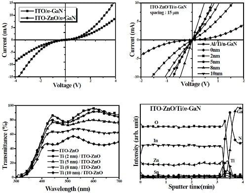
The
I-V curves of the as-deposited ITO and cosputtered ITO-ZnO films’ contact to the
n-GaN epilayer, respectively, measured from the contact spacing of 15 μm are shown in
Figure 2. Both of these contact systems exhibited nonlinear characteristics even though the cosputtered ITO-ZnO film’s contact to the
n-GaN epilayer had a lower series resistance at an applied voltage of 2 V (~485 Ω) than the ITO/
n-GaN contact system (~784 Ω). The rectifying properties with significant leakage currents measured from these contact systems occurred because of the large discrepancy in work functions between the transparent electrode and the
n-GaN epilayer [
14]. A post-annealing treatment was conducted on these contact systems for the purpose of making these structures become ohmic contacts.
Figure 3a,b, respectively, give the
I-V curves of ITO/
n-GaN and ITO-ZnO/
n-GaN contact systems processed by a rapid thermal annealing (RTA) treatment at various temperatures for 1 min under vacuum ambient, measured from the contact spacing of 15 μm. The currents of both of these contact systems were apparently increased as the annealing temperature was increased. The largest current at a bias of 2 V was obtainable from the 200 °C–annealed ITO/
n-GaN contact system, while that of the ITO-ZnO/
n-GaN contact system occurred at an annealing temperature of 300 °C. However, although the series resistance of the 300 °C–annealed ITO-ZnO/
n-GaN contact system was decreased significantly to about 200 Ω at a bias of 2V, its
I-V curve still was somewhat insufficient for achieving ohmic contact. In contrast to the ITO-ZnO/
n-GaN contact system, the as-deposited metallic Ti/Al contact to the
n-GaN epilayer exhibited a good, linear
I-V characteristic without the requirement of a post-annealing process, as shown in
Figure 4a. The specific contact resistance derived from the resistance of the Al/Ti/
n-GaN contact system as a function of the contact spacing in the set figure was approximately 5.1 × 10
−5 Ω·cm
2. The mechanism responsible for the achievement of the nonalloyed ohmic contact behavior using the metallic Ti/Al structure mainly was due to the elemental Ti, which possessed a much lower work function (ϕ = 4.3 eV). This value was only a little higher than the work function of
n-GaN (ϕ = 4.1 eV) as compared to that of the transparent ITO (ϕ = 5.1 eV) [
15,
16]. In addition, since the electron carriers correlated with the nitrogen vacancies (V
N) at the
n-GaN surface would be increased as a consequence of the Ti atom, Ti was beneficial for inducing the outdiffusion of the nitrogen atoms at the
n-GaN surface.
Figure 4b shows the elemental distributions over the Ti/
n-GaN interface conducted from the AES depth profile. The outdiffusion of the N atoms was observed clearly at the Ti/
n-GaN interface, resulting in the increase in the electron concentration at the
n-GaN surface associated with large amounts of the V
N donors [
17,
18].
The above-mentioned structures’ contact to the
n-GaN epilayer demonstrated that the transparent electrodes, such as ITO and cosputtered ITO-ZnO films, have a nonlinear
I-V curve even when annealed at an elevated temperature, whereas the opaque Ti/Al system had ohmic contact behavior when contacting the
n-GaN epilayer without a post-annealing treatment. Therefore, we employed a thin Ti interlayer which was deposited between the interface of ITO-ZnO and
n-GaN to achieve a true ohmic contact system with optical transparency at the visible wavelengths.
Figure 5a shows the
I-V characteristics of the ITO-ZnO/Ti/
n-GaN contact systems as a function of the thickness of the Ti interlayer, measured from the contact spacing of 15 μm (the
I-V curve of the Al/Ti/
n-GaN contact system also is shown for comparison). The cosputtered ITO-ZnO film directly contacted the
n-GaN epilayer, which resulted in a nonlinear
I-V property that became an ohmic contact behavior when a thin Ti interlayer was deposited prior to the deposition of the cosputtered ITO-ZnO film. The current flow of the nonalloyed ITO-ZnO/Ti/
n-GaN contact system was increased initially as the thickness of the Ti interlayer increased, but it decreased as the thickness of the Ti interlayer reached 10 nm. It was worth noting that the current of the ITO-ZnO/
n-GaN contact structure inset by an 8-nm-thick Ti interlayer at a bias of 2 V obviously was higher than that of the metallic Ti/Al structure’s contact to the
n-GaN epilayer. The evolution of the specific contact resistance as a function of the Ti interlayered thickness in the ITO-ZnO/Ti/
n-GaN contact system is illustrated in
Figure 5b. The specific contact resistances of these ITO-ZnO/Ti/
n-GaN contact systems as well as the Ti/Al ohmic contact to the
n-GaN epilayer are summarized in
Table 2. A specific contact resistance of 2.5 × 10
−3 Ω·cm
2 was obtainable from the cosputtered ITO-ZnO film’s contact to the
n-GaN epilayer with an additional 2-nm-thick Ti interlayer inset between the interface of ITO-ZnO and
n-GaN. As the thickness of the Ti interlayer reached 8 nm, the specific contact resistance was optimized further to 4.8 × 10
−5 Ω·cm
2, a value that was a little better than that of the metallic Ti/Al contact to the
n-GaN epilayer. The optical transmittances of these Ti/ITO-ZnO systems with various Ti interlayered thicknesses are given in
Figure 6 (the optical transmittance of the cosputtered ITO-ZnO film also is shown for comparison). The thin Ti interlayer did not change the onset absorption of the cosputtered ITO-ZnO film at the near-UV wavelength. However, the optical transparency of the Ti/ITO-ZnO systems was reduced gradually as the thickness of the Ti interlayer increased. The average transmittances at the visible wavelengths of these Ti/ITO-ZnO systems are listed in
Table 2. It can be found that the average transmittances of these Ti/ITO-ZnO systems decreased monotonously from 83.2% to 48.8% as the thickness of the Ti interlayer was increased from 2 to 10 nm. Accordingly, although the cosputtered ITO-ZnO film’s ohmic contact to the
n-GaN epilayer can be optimized when an 8-nm-thick Ti interlayer is inset between the ITO-ZnO/
n-GaN interface, the structural transmittance at the visible wavelengths apparently decreased to 63.2% as compared to the cosputtered ITO-ZnO film (~84.6%). Herein, we proposed the figure of merit (FOM), Φ, to quantitatively determine the performance of these transparent electrodes’ ohmic contact to the
n-GaN epilayer. This value is calculated according to the following expression which takes into consideration both the specific contact resistance, ρ
c, and the average optical transmittance,
Tave [
19,
20]:
The higher the FOM of the Ti/ITO-ZnO system obtained, the better the quality of the transparent electrode contacted to the
n-GaN epilayer.
Table 2 gives the FOM of the Ti/ITO-ZnO systems as a function of the thickness of the Ti interlayer. A highest FOM of 203 was achieved from the Ti/ITO-ZnO system with an 8-nm-thick Ti interlayer contacting the
n-GaN epilayer. Moreover, the FOM obviously was reduced to a value lower than unity for the cosputtered ITO-ZnO film’s contact to the
n-GaN epilayer while inset by a 10-nm-thick Ti interlayer. This was the result of both the specific contact resistance and average optical transmittance being apparently inferior to that of the sample inset by a Ti interlayer with the thickness of 8 nm.
Figure 7a,b show the elemental distributions of the cosputtered ITO-ZnO film directly contacting the
n-GaN epilayer and an 8-nm-thick Ti interlayer inset between the interface of ITO-ZnO and
n-GaN, respectively. The cosputtered ITO-ZnO film’s contact to the
n-GaN epilayer had significant interdiffusion at the ITO-ZnO/
n-GaN interface, especially for the O and N atoms. The outdiffusion of the N atoms at the
n-GaN surface led to an increase in the electron carriers at the
n-GaN surface, whereas the indiffusion of the O atoms to the
n-GaN surface from the ITO-ZnO film was proven to result in the compensation of the carriers and impede the carrier transmission, thereby exhibiting the Schottky property, as shown in
Figure 3. In contrast to the cosputtered ITO-ZnO film directly contacting the
n-GaN epilayer, a thin Ti interlayer inset between the interface of ITO-ZnO and
n-GaN resulted in more N atoms being outdiffused from the
n-GaN surface, as shown in
Figure 7b. In addition, the indiffusion of the O atoms to the
n-GaN epilayer, which was harmful to the carriers’ transmission, was depressed by the additive Ti interlayer. Accordingly, this nonalloyed ITO-ZnO/Ti/
n-GaN contact system had excellent ohmic contact behavior with optical transmittance.


