Article

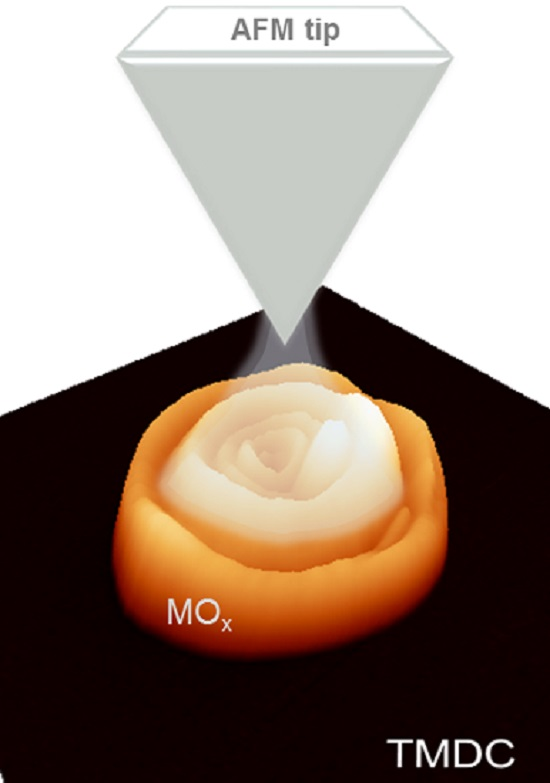
Local Oxidation Nanolithography on Metallic Transition Metal Dichalcogenides Surfaces

by
Elena Pinilla-Cienfuegos
1,*,†,
Samuel Mañas-Valero
1,
Efrén Navarro-Moratalla
1,‡,
Sergio Tatay
1,2,
Alicia Forment-Aliaga
1,* and
Eugenio Coronado
1
1
Instituto de Ciencia Molecular, Universitat de València, Calle Catedrático José Beltran, 2, Paterna, Valencia 46980, Spain
2
Unité Mixte de Physique CNRS/Thales, Univ. Paris-Sud, Université Paris-Saclay, Palaiseau 91767, France
*
Authors to whom correspondence should be addressed.
Submission received: 27 July 2016 / Revised: 25 August 2016 / Accepted: 29 August 2016 / Published: 8 September 2016
(This article belongs to the Special Issue Two-Dimensional Transition Metal Dichalcogenides)

Abstract

:
The integration of atomically-thin layers of two dimensional (2D) materials in nanodevices demands for precise techniques at the nanoscale permitting their local modification, structuration or resettlement. Here, we present the use of Local Oxidation Nanolithography (LON) performed with an Atomic Force Microscope (AFM) for the patterning of nanometric motifs on different metallic Transition Metal Dichalcogenides (TMDCs). We show the results of a systematic study of the parameters that affect the LON process as well as the use of two different modes of lithographic operation: dynamic and static. The application of this kind of lithography in different types of TMDCs demonstrates the versatility of the LON for the creation of accurate and reproducible nanopatterns in exfoliated 2D-crystals and reveals the influence of the chemical composition and crystalline structure of the systems on the morphology of the resultant oxide motifs.

Graphical Abstract

1. Introduction

The implementation of nanotechnology in real world applications relies on the use of accurate and simple lithographic techniques that permit the preparation of nanodevices. In this scenario, lithography based on Scanning Probe Microscopy (SPM) [1,2] has become very important due to its versatility, opening the door to new approaches such as the scratching or shaving of surfaces, the controlled deposition of material, or the realization of local chemical reactions. In particular, local oxidation nanolithography (LON) [3,4,5] a.k.a Local Anodic Oxidation (LAO) or Oxidation Scanning Probe Lithography (o-SPL), has been broadly used; under controlled ambient humidity conditions, when a bias voltage is applied between the tip of the microscope and the sample, a confined water meniscus is created by capillary condensation at the tip-surface interface. This confinement area acts as an electrochemical cell where an oxidation reaction takes place. The tip works as the cathode, the water acts as the electrolyte and the sample plays the role of the anode (oxidation reaction), so the chemical reaction gives rise to the formation of an oxide feature (see schematics at Figure 1a). The technique has been also extended to other liquids, which changes the nature of the patterned motifs, giving rise for example, to carbon-based features that can be used as etching resistant [6].
Since the first nano-oxidation lithography performed on silicon by Dagata et al. in 1990 [3], a large number of materials have been lithographed with oxide motifs, i.e., metals, semiconductors, organic surfaces or layered crystals like Transition Metals Dichalcogenides (TMDCs) [7,8,9]. Thus, as a result of the interest awakened by the isolation of real 2D systems from bulk laminar crystals, LON was also extended to single layers with the formation of oxide patterns on graphene [10]. By means of this accurate lithography it is possible, for instance, to pattern graphene nanoribbons opening a band gap which permits the implementation of graphene in field effect transistors [11]. Regarding TMDCs, analogous nano-oxidation processes have been performed on semiconducting 2D-TMDCs, for example, by the selectively oxidation via oxygen plasma of MoS2 [12] and by the laser-oxidation procedure of multilayer TaSe2 [13] or WSe2 [14]. However few examples can be found in the literature that use LON on ultrathin layers of TMDCs, namely the patterning of ultrathin metallic TaS2 flakes [15], and the local oxidation of semiconducting MoS2 layers [16]. Yet, the rich chemical tuneability and (opto)electronic properties that one can find within the TMDC family could provide new interesting platforms for the application of LON. Given the wide variety of applications that TMDCs have found nowadays in fields such as energy storage, optoelectronics, or biosensors [17,18], LON could be a powerful tool to facilitate the structuration and integration of 2D crystals in devices or multifunctional systems. Interestingly, the ability to nanostructure thin superconducting TMDC layers by LON could be employed for the manipulation of the vortex state (in an attempt to modify the vortex pinning and to enhance the critical parameters, such as the critical current or the critical temperature) [19], and to address the appearance of novel vortex phases or the control of the vortices dynamics for developing new devices based on the flow of magnetic fluxons [20].
In this scenario, we have performed a comprehensive study of the influence of different oxidation parameters that affect the LON process, such as the tip velocity or the tip-to-sample distance, using 2H-TaS2 flakes as the target material. Additionally, we have also studied the oxidation process on other metallic systems (which are superconductors at low temperatures): 2H-TaSe2, 2H-NbSe2 and 2H-NbS2; where we analyze the material-dependent oxidation patterns observed.

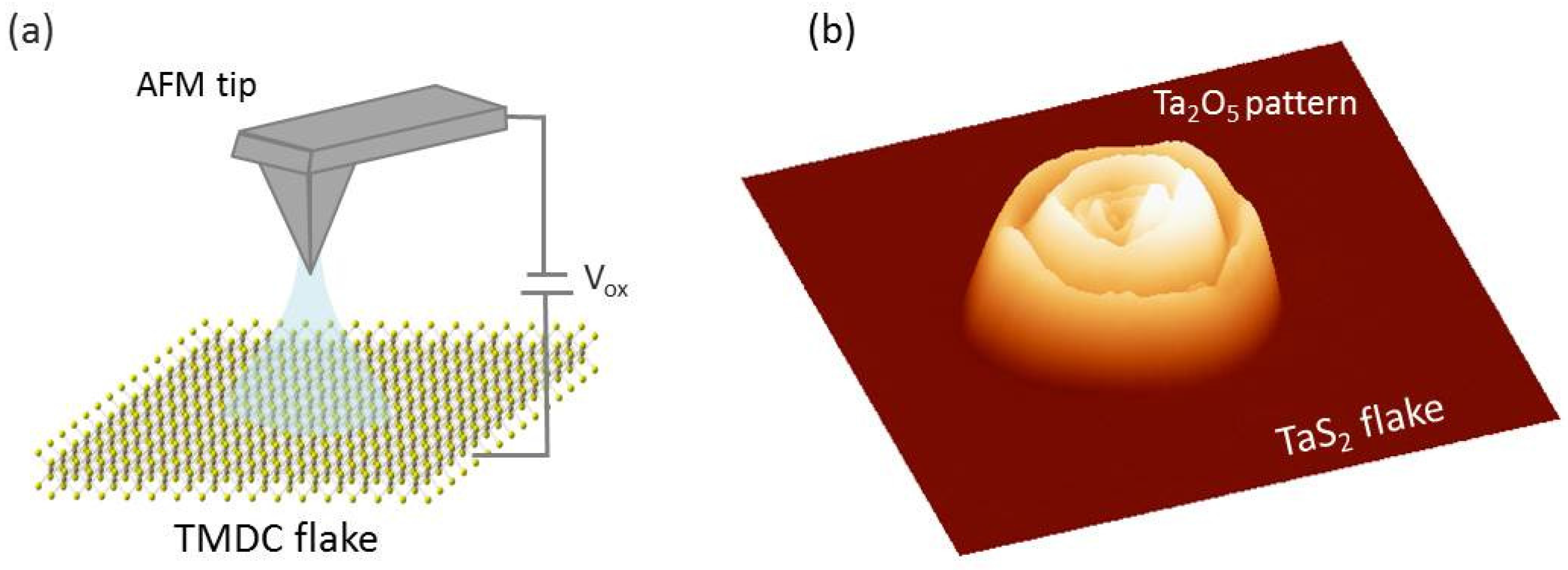
2. Materials and Methods

(1) Synthesis of TMDCS Single Crystals
The crystal growth of TMDCs was performed by chemical vapor transport (CVT). In a first step, powders of the metal and the chalcogen were mixed in a stoichiometric ratio in an evacuated sealed quartz ampoule (P ~10−5 mbar) and heated at high temperatures (typically, at 900 °C during 9 days). Secondly, the obtained polycrystalline material was mixed with iodine as a transport agent in an evacuated sealed quartz ampoule (P ~10−5 mbar) and heated in a gradient of temperature in a three-zone furnace. Phase purity was confirmed by X-ray powder diffraction (XRPD). More details regarding the crystal growth and characterization of the different TMDCs can be found in the Supplementary Materials S1.
(2) Substrate Cleaning
Si wafers were purchased from Dxl Enterprises, Inc. (Mahwah, NJ, USA). Before any LON experiment, the substrates were cleaned and simultaneously activated by three 10 min sonication cycles (Ultrasonic cleaner: a BRANASONIC MTH-5510 ultrasonic cleaner, 185 W) in diluted basic piranha solution: NH4OH (conc.):H2O2:H2O, 1:1:2 (v/v/v). Between each sonication cycle the substrates were rinsed in water and immersed in a fresh aliquot of piranha solution. The substrates were finally washed by sonication in ultrapure milli-Q water (Millipore S.A.S., Molsheim, France) during 10 mins. Finally, the substrate was thoroughly blow dried before used.
(3) Optical Microscope
General optical microscopy images were taken using a Nikon D-600 SLR camera (Nikon Instruments Europe BV, Amsterdam, Netherlands) mounted on the trinocular stage of a Nikon LV-100 optical microscope (Nikon Instruments Europe BV, Amsterdam, Netherlands). The microscope was equipped with a Nomarski prism for DIC contrast imaging and with five Nikon PLAN FLUOR EPI objectives (Nikon Instruments Europe BV, Amsterdam, Netherlands): 5× (numerical aperture, NA = 0.15), 10× (NA = 0.3), 20× (NA = 0.45), 50× (NA = 0.8), 100× (air, NA = 0.9). The calibration of the SLR camera with the 5× and the 10× objective objectives was performed with a reference millimeter reticle, resulting in a lateral space calibration value of 95.3 μm·px−1 and 47.8 μm·px−1. The higher power lenses were calibrated using an AFM calibration grid with a period of 10 μm, resulting in the following values: 238.0 μm·px−1, 95.2 μm·px−1 and 47.4 μm·px−1 for the 20×, the 50× and the 100× objectives respectively.
(4) Atomic Force Microscopes (AFM) and Local Oxidation Nanolithography (LON) Equipment
Two different AFMs were used for the local oxidation nanolithography on TaS2. One is a Nanoscope IVa (Bruker, Karlsruhe, Germany) interfaced with a home-made voltage amplifier. In this instrument, the nanolithography was made by programming simple patterns (dots, lines, and matrices) in C++. The other one is a Cervantes Fullmode SPM (Nanotec Electrónica S.L., Madrid, Spain) using the AFM mode, that provides powerful nanolithography software WSxM (WSxM 5.0 Develop 7.0, Nanotec Electrónica S.L., Madrid, Spain) [21]. This software permits plotting customized pre-loaded patterns as well as simple patterns. All experiments were carried out at room temperature and the ambient relative humidity of 40%–70% by employing a commercial bench-top humidifier.
In both AFMs, a vertical optical microscope is used to visualize the tip over the surface, being able to position the tip on top of the selected flake. The topographic characterization of the surface is made in Tapping mode, which is a non-invasive mode of operation. The same silicon probes of fr ≈ 300 KHz and k ≈ 40 N/m (PPP-NCH, Nanosensors, Neuchatel, Switzerland)) were used for the morphological characterization as well as for performing the LON.
(5) Conducting-Tip Atomic Force Microscope (CT-AFM)
CT-AFM was performed under N2 atmosphere on a Veeco Enviroscope (Bruker, Karlsruhe, Germany) multimode AFM equipped with a Digital Instruments NanoScope IV controller (Bruker, Karlsruhe, Germany). This apparatus was modified by Houzé et al. to perform local resistance measurements in the range of 102–1012 Ohms under a bias voltage ranging from 0.1 to 10 V, with 5% accuracy [22]. In this set-up, the conductive tip is electrically polarized and the current flowing through the sample is amplified, converted in a voltage related to the resistance (V α log(R)) and analyzed by the Nanoscope IV's controller. In these experiments samples were contacted to a sample holder with conducting silver paint and boron-doped polycrystalline diamond coated Si3N4 tips with spring constant k ≈ 40 N/m (Bruker) were used to scan the sample in contact mode while performing the resistance mapping at an applied bias of 2 V.

3. Results and Discussion

3.1. AFM LON on TaS2 Surfaces

The TaS2 flakes were transferred to freshly base-activated Si p-doped substrates by a micro-mechanical exfoliation technique developed by us [23]. Both thick and ultrathin TaS2 flakes were obtained making it possible to study the LON results as a function of the number of layers.

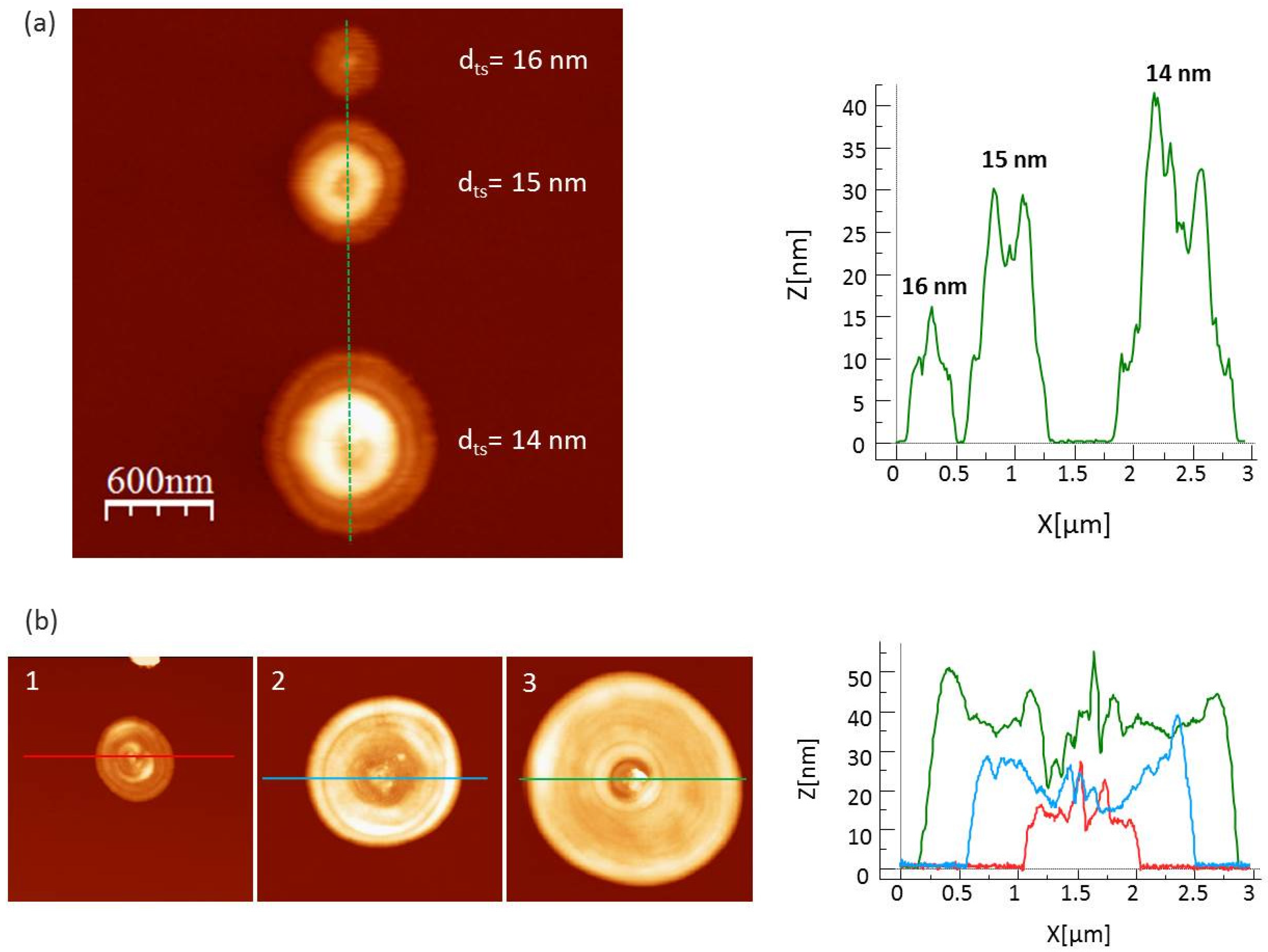
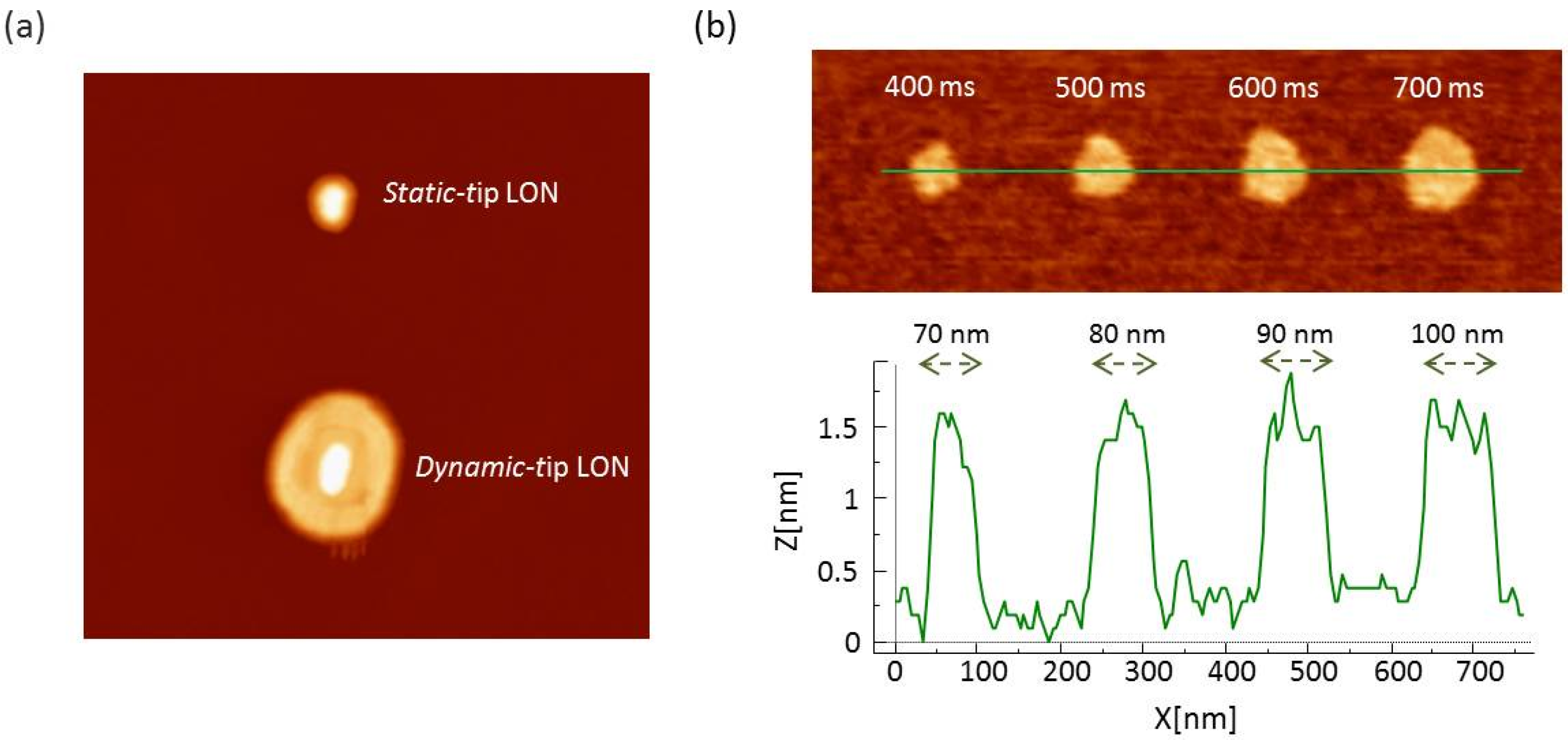
3.1.1. Dynamic-Tip LON

The AFM-LON studies were first conducted using the classical oxidation procedure in which the tip is oscillating during the process (dynamic-tip LON). In these samples, the LON produced massive oxide formations with a rippled topography (Figure 1b). This ripple oxide formation by dynamic-tip LON was found to be very sensitive to the experimental conditions. Oxide dots created at the same values of voltages and times exhibit not only different topologies (different number of rings) but also different heights and widths.
This observation can be related to the fact that the size of an oxide pattern by LON generally depends on the size of the meniscus, and this is dependent on the tip-to-sample distance (among other parameters). Shorter tip-substrate spacing favors the formation of the water meniscus while an increase in the tip-to-sample distance leads to a linear decrease in the meniscus width [24,25]. In our case, the tip-to-sample distance was found to have a threshold value from which the size of the pattern grew significantly as can be seen in Figure 2a. The tip-to-sample distance was checked by recording the so called force-distance curve. This distance can be adjusted by choosing the corresponding amplitude of oscillation and by fitting the set point in tapping mode. In general, a set point of 1.5 V was initially tuned in order to achieve a reasonable surface proximity for LON purposes. As the tip-to-sample distance was decreased, the oxide width and height grew. The standard 12–14 nm tip-to-sample distances led to precise nano-dot writing. As the tip was pushed closer to the surface, uncontrolled massive oxide formations were fabricated. Interestingly, it was also observed that the number of the outer rings of the ripple formations grew in an inversely proportional manner with respect to the tip sample distance: three outer rings for dts = 14 nm, two outer rings for dts = 15 nm and a single outer ring for dts = 16 nm. So for a bigger water meniscus (shorter tip-to-sample distance), a bigger oxide motif is formed and there is more space for the formation of a ripple structure with a larger number of rings.
As observed for other materials [26], it was also found that there is always a threshold potential from which the oxide started to form. Then, at a constant tip-sample distance, the size of the whole pattern is governed by the pulse time duration (tox). In Figure 2b it is shown a set of three oxidized dots performed at dts ~13 nm and voltage pulse, Vox = −21 V, with increasing time of oxidation 100 ms, 200 ms, 300 ms, respectively. The formations grew in number of rings, height and width as the pulse time was increased.
Finally, some experiments were performed at a positive bias instead of a negative bias and similar results were obtained. As expected, the polarity of the voltage pulse did not affect the oxidation outcome given the metallic nature of the TaS2 conducting flakes [27].

3.1.2. Static-Tip LON

As already demonstrated in a previous study [15] a modification of the regular dynamic-tip LON was used to perform accurate and reproducible patterns. In this case, instead of oxidizing in tapping mode, a static oxidation method was developed in which the oscillation amplitude was stopped during the application of the voltage pulse (static-tip LON). This new methodology affords a higher degree of control of the morphology and profiles of the patterned structures by fine-tuning the oxidation conditions (Figure 3a). Although we do not have yet a theoretical study that confirms our hypothesis, we can suggest based on the experimental observations, that the oscillation induces a less controllable oxide dot, probably due to the change in size of the water capillary during the oxidation process in the dynamic-tip mode oxidation that enlarge the oxidation area because the tip-to-sample distance is changing during the oscillation. However, in the static-tip mode the tip-to-sample distance remains constant, reaching a better control on the pattern shape. (See a schematic carton describing both processes in the Supplementary Materials, Figure S2). Further experiments were directed toward optimizing the precision of the static-tip oxidation by adjusting the pulse duration and the applied voltage, while maintaining a constant humidity and tip-sample distance. It appears that the height and the final area of the oxidized pattern directly depend on the voltage and time pulse, respectively. Once again, threshold potentials were found to be very sensitive to experimental instant conditions, varying in the approximately same range as for dynamic-tip oxidation. Once the threshold voltage was established, the resulting oxide sizes could be precisely controlled by adjusting the pulse duration (Figure 3b). In order to assure a precise oxidation of sub-nanometric features on the surface, pulse times within the tens of millisecond time-scale were required.
Once the proper working parameters are set, static-tip LON enabled a uniform and reproducible patterning of oxide motifs on large surface areas of thick 2H-TaS2 flakes. Figure 4a shows the high reproducibility reached with the static-tip mode. To illustrate the uniformity reached, the 1040 oxide nanodots, could be fitted to a Gaussian distribution with a standard deviation as small as 0.15 nm. This result is comparable with the precision reached with dynamic-tip LON performed on silicon [28]. The improved control over the patterning technique achieved via static-tip LON opened the door to the oxidation of ultrathin few layer TaS2 samples (<5 nm) [15]. Nevertheless, regardless of the high level of precision that can be achieved in static mode, long pulse durations and high values of voltage pulses, gave rise to oxide motifs that exhibit the characteristic rippled structure already observed in dynamic-tip LON.
Finally, it was also found that the oxidation performed at lower scan speeds produced higher oxide motifs than the ones obtained scanning at faster speeds. A height profile taken in Figure 4b (performed at v = 100 nm/s) and 4c (performed at v = 500 nm/s) is shown in Figure 4d, where it can be clearly seen that the faster scans give rise to lower dots than the slower scans.

3.2. Characterization of LON Motifs Patterned on 2H-TaS2

3.2.1. Etching Experiments

As it occurs for other materials (LON in silicon, for example), the oxide created by LON does not only grow above the surface but also propagates towards the underlying layers of the material creating a 3D pattern. Direct evidence of the bulk characteristics of the oxide motifs created on TaS2 could be observed by immersing the samples in an HF solution to selectively etch the oxidized motifs (Figure 5). These experiments confirmed that the wave-like nature of the oxidation mechanism on TaS2 was transferred into the silicon substrate; this can be clearly observed for the case of the thinner crystals (Figure 5b and Figure S3). For the thicker samples we notice that the oxide growth outside the surface is slightly higher than the oxidation inside the sample, in a similar way to what is observed for the LON on Si, where 60% of the oxide is above the substrate baseline [29].

3.2.2. Electrical Properties of the Ultrathin TaS2 Layers

To probe the conducting behavior of the deposited flakes and the material growth on the generated motifs, conducting tip AFM (CT-AFM) was performed on oxidized and non-oxidized TaS2 flakes.
First, the resistance map of a flake with different thicknesses deposited on doped silicon was measured. When a 2 V bias was applied between the tip and the surface during contact scanning, a clear contrast in the conductance between TaS2 flakes and the surface was observed (Figure 6). The entire TaS2 surface appeared to have the same conducting behavior and therefore, no effect of the flake thickness was observed (Figure 6b). The electrical properties of the oxide motifs patterned via LON on top of TaS2 layers were also probed. As expected, a clear contrast was observed between conductive pristine and insulating oxidized regions (Figure 6d). The big difference in conductivity makes these TaS2/Ta2O5 heterostructures surfaces excellent candidates for the fabrication of circuitry at the nanoscale and also for more advanced lower temperature applications profiting from the superconducting properties of TaS2 layers.

3.3. LON on Other TMDCs

The AFM-LON was also performed in other type of TMDCs in order to elucidate the unusual growth mechanism found for the TaS2 and to extend the method for the fabrication of heterostructures for future applications.
The selected TMDCs were: TaSe2, NbSe2, and NbS2. As well as TaS2, all of them exhibit a metallic behavior at room temperature and superconducting type II at low temperature. They were conveniently exfoliated from CVT crystals by micromechanical exfoliation with the technique above mentioned, and transferred on to freshly base-activated Si p-doped substrates. Each sample preparation was always done just before performing the LON experiment following the same procedure used for the TaS2.
After applying similar oxidation parameters in dynamic-tip LON mode, rippled motifs similar to the concentric rings obtained in TaS2 were also observed on NbS2. However, for the case of selenide compounds (TaSe2 and NbSe2), oxide motifs of a central spot surrounded by a single ring with a nipple shape were always produced. This kind of feature reminds of the oxide growth on silicon and on certain polymers caused by a nano-explosion followed by a shockwave (Figure 7) [30]. It is worthy to mention that by means of applying a voltage with an AFM tip on the semiconducting TMDCs MoS2 [31] and WSe2 [32], different types of structures have been achieved, that also resemble the patterns presented in this work. However in both cases, authors highlight the non-oxide nature of the motifs, against the results observed by us that prove the oxide nature of the obtained patterns on above mentioned metallic TMDCs (i.e.: HF etching experiments and spectroscopic measurements in [15]).
During the exfoliation process of NbS2 crystals, it was observed that the characteristic TMDCs platelet-like flakes were mixed with needle-like stacks. From the transmission electron microscopy analysis of these needles, we could infer the rhombohedral phase 3R of the NbS2 (for detailed characterization see the Supplementary Materials S1). The local oxidation of this new system gave rise to a unique case of dendritic oxide growth (Figure 8a,b). Instead of the expected rippled mounds, dendritic shaped oxides that formed a fractal pattern were obtained on the needle. A range of oxidation parameters were utilized to create different sizes although all of them appeared to have the dendritic structure. While applying less voltage and shorter time pulses, the formations obtained were more rounded and smaller in size (Figure 8c-1), very high voltages (> −30 V) applied during 100 ms or more, derived in an uncontrolled oxide branched formation that grew several microns all over the surface until reaching the limits of the needle (Figure 8c-2). As observed for the rippling formations, the dendritic oxides always stopped at the edges of the crystal. The experiment was repeated in different needle-like stacks of 3R-NbS2 and always a dendritic growth was obtained (Figure 8d–f). The dendrites have a central circular spot just right below the site were the AFM tip makes the discharge and then, it seems to evolve through avalanches like the ripple formations of the rest of the TMDCs studied. This anomalous structure could be due to an oxidation process taking place across the planes in the needle-like exfoliated crystals. Etching experiments were carried out to ascertain the 3D nature of this type of oxide formations. As can be seen in Figure 8f, the etching reveals a 3D pattern that grew deep inside the 3R-NbS2. In this case, the 50% of the oxide grows above the substrate baseline.
Finally, the static-tip LON experiments were also performed in NbSe2 demonstrating the possibility of patterning very small oxide motifs with high accuracy and reproducibility. Moreover, by the fine adjustment of the LON parameters, we were capable to oxidize a large area of 12.5 µm2 with a matrix of 20 × 20 dots of average heights of 1 nm (See Figure S4) proving that it is a general LON method that could be extended to any exfoliated TMDC.

4. Conclusions

In this work, we have demonstrated that it is possible to use the formation of well-defined oxide motifs to pattern metallic TMDCs flakes of different composition and thicknesses. After exceeding a voltage threshold, the size of the oxide dot has the usual dependence with humidity, tip-to-sample distance, tox, Vox and scan speed observed in other materials like silicon. Interestingly, the morphology of the oxide feature seems to change with the nature of the chalcogenide, and the phase of the material, giving rise to nipple shapes, concentric rings, or even dendritic structures.
The formation of a unique outer ring surrounding a central oxide spot observed in TaSe2 and NbSe2 is an anomaly that has been also observed for semiconducting Si substrates and insulating polymers [30]. For LON on TaS2 and NbS2 surfaces, various concentric symmetrical rings were formed instead of a unique ring. The number of rings grew with the lateral size of the oxide motif and this rippled formation is only observed for the sulphide materials. It has been shown that the LON experiments performed onto the needle–like 3R-NbS2 crystals behave completely different from the rest. In this case, a dendritic growth has been found that could be explained if the oxidation process takes place across the crystal planes instead of on top of a single plane. Unfortunately, we still do not have a complete explanation about the mechanisms responsible of these different morphologies and they are currently under study.
The pattering of large areas (µm2) with nanometric motifs over exfoliated TMDCs crystals gives rise to the combination of materials with completely different properties (e.g., superconducting/isolating) that can be seen as multifunctional horizontal heterostructures. In addition, this formation of the oxide patterns could permit the study of vortex formation and dynamics in 2D superconducting materials. The possibility of creating these pinning centers by static-tip LON with high reproducibility and accuracy in flakes with different thicknesses opens the door for the study of the thickness-dependent vortex dynamics on superconducting TMDC.

Supplementary Materials

The following are available online at https://0-www-mdpi-com.brum.beds.ac.uk/2076-3417/6/9/250/s1. Figure S1.1: 2H-TaS2 XRPD pattern (green) and unit cell refinement (blue). Peaks positions are marked with vertical red lines and the background with a black line. Figure S1.2: 2H-TaSe2 XRPD pattern (green) and unit cell refinement (blue). Peaks positions are marked with vertical red lines and the background with a black line. Figure S1.3: 2H-NbS2 XRPD pattern (green) and unit cell refinement (blue). Inset: Photography of a 2H-NbS2 crystal. Peaks positions are marked with vertical red lines and the background with a black line. Figure S1.4: TEM characterization of 3R-NbS2 needles. (a) TEM image of the inspected needle; (b) detail with atomic scale area; and (c) TEM FFT diffraction pattern of (b). Figure S1.5: 2H-NbSe2 XRPD pattern (green) and unit cell refinement (blue). Peaks positions are marked with vertical red lines and the background with a black line. Figure S2: Sketch describing AFM tip movement during dynamic-tip LON and static-tip LON processes. Figure S3: Etching in thin flakes. Figure S4: AFM topography image of a matrix of 20 × 20 oxide dots onto the NbSe2 surface by static-tip LON. Image size: 12.5 µm × 12.5 µm.

Acknowledgments

We acknowledge the financial support from the Spanish MINECO (MAT2014-56143-R co-financed by FEDER and Excellence Unit “María de Maeztu” MDM-2015-0538), the EU (2D-INK-664878), and the Generalidad Valenciana (Program Prometeo). Samuel Mañas-Valero thanks the Spanish MINECO for the F.P.U. fellowship and Alicia Forment-Aliaga thanks the Universitat de València for a Research grant.

Author Contributions

E.P.-C., E.N.-M., A.F.-A. and E.C. conceived and designed the experiments; E.N.-M. synthesized the TMDCs crystals; E.P.-C., S.M.-V., and E.N.-M. performed the LON experiments; S.T. performed the CT-AFM experiments and analyzed the data. E.P.-C., A.F.-A. and E.N.-M. analyzed the LON and AFM data. E.P.-C. and A.F.-A. wrote the article and all authors contributed to corrections and discussion.

Conflicts of Interest

The authors declare no conflict of interest.

References

  1. Garcia, R.; Knoll, A.W.; Riedo, E. Advanced scanning probe lithography. Nat. Nanotechnol. 2014, 9, 577–587. [Google Scholar] [CrossRef] [PubMed]
  2. Xie, X.N.; Chung, H.J.; Sow, C.H.; Wee, A.T.S. Nanoscale materials patterning and engineering by atomic force microscopy nanolithography. Mat. Sci. Eng. 2006, 54, 1–48. [Google Scholar] [CrossRef]
  3. Dagata, J.A.; Schneir, J.; Harary, H.H.; Evans, C.J.; Postek, M.T.; Bennett, J. Modification of hydrogen-passivated silicon by a scanning tunneling microscope operating in air. Appl. Phys. Lett. 1990, 56, 2001–2003. [Google Scholar] [CrossRef]
  4. Wendel, M.; Irmer, B.; Cortes, J.; Kaiser, R.; Lorenz, H.; Kotthaus, J.P.; Lorke, A.; Williams, E. Nanolithography with an atomic force microscope. Superlattices Microst. 1996, 20, 349–356. [Google Scholar] [CrossRef]
  5. Garcia, R.; Calleja, M.; Perez-Murano, F. Local oxidation of silicon surfaces by dynamic force microscopy: Nanofabrication and water bridge formation. Appl. Phys. Lett. 1998, 72, 2295–2297. [Google Scholar] [CrossRef] [Green Version]
  6. Suez, I.; Backer, S.A.; Fréchet, J.M.J. Generating an etch resistant “resist” layer from common solvents using scanning probe lithography in a fluid cell. Nano Lett. 2005, 5, 321–324. [Google Scholar] [CrossRef] [PubMed]
  7. Yamamoto, M.; Dutta, S.; Aikawa, S.; Nakaharai, S.; Wakabayashi, K.; Fuhrer, M.S.; Ueno, K.; Tsukagoshi, K. Self-limiting layer-by-layer oxidation of atomically thin WSe2. Nano Lett. 2015, 15, 2067–2073. [Google Scholar] [CrossRef] [PubMed]
  8. Böhmisch, M.; Burmeister, F.; Boneberg, J.; Leiderer, P. Nanostructuring on WSe2 with the atomic force microscope by a potential controlled electrochemical reaction. Appl. Phys. Lett. 1996, 69, 1882–1884. [Google Scholar] [CrossRef]
  9. Tsai, J.T.H.; Hsu, C.-Y.; Hsu, C.-H.; Yang, C.-S.; Lin, T.-Y. Fabrication of resistive random access memory by atomic force microscope local anodic oxidation. NANO Brief Rep. Rev. 2015, 10, 1550028–1550036. [Google Scholar] [CrossRef]
  10. Weng, L.; Zhang, L.; Chen, Y.; Rokhinson, L. Atomic force microscope local oxidation nanolithography of graphene. Appl. Phys. Lett. 2008, 93. [Google Scholar] [CrossRef]
  11. Masubuchi, S.; Ono, M.; Yoshida, K.; Hirakawa, K.; Machida, T. Fabrication of graphene nanoribbon by local anodic oxidation lithography using atomic force microscope. Appl. Phys. Lett. 2009, 94. [Google Scholar] [CrossRef]
  12. Choudhary, N.; Islam, M.R.; Kang, N.; Tetard, L.; Jung, Y.; Khondaker, S. Two-dimensional lateral heterojunction through bandgap engineering of MoS2 via oxygen plasma. J. Phys. Condens. Matter. 2016, 28. [Google Scholar] [CrossRef] [PubMed]
  13. Cartamil-Bueno, S.J.; Steeneken, P.G.; Tichelaar, F.D.; Navarro-Moratalla, E.; Venstra, W.J.; Van Leeuwen, R.; Coronado, E.; Van Der Zant, H.S.J.; Steele, G.A.; Castellanos-Gomez, A. High-quality-factor tantalum oxide nanomechanical resonators by laser oxidation of TaSe2. Nano Res. 2015, 8, 2842–2849. [Google Scholar] [CrossRef]
  14. Tan, C.; Liu, Y.; Chou, H.; Kim, J.-S.; Wu, D.; Akinwande, D.; Lai, K. Laser-assisted oxidation of multi-layer tungsten diselenide nanosheets. Appl. Phys. Lett. 2016, 108. [Google Scholar] [CrossRef]
  15. Coronado, E.; Forment-Aliaga, A.; Navarro-Moratalla, E.; Pinilla-Cienfuegos, E.; Castellanos Gomez, A. Nanofabrication of TaS2 conducting layers nanopatterned with Ta2O5 insulating regions via AFM. J. Mater. Chem. C 2013, 1, 7692–7694. [Google Scholar] [CrossRef]
  16. Espinosa, F.M.; Ryu, Y.K.; Marinov, K.; Dumcenco, D.; Kis, A.; Garcia, R. Direct fabrication of thin layer MoS2 field-effect nanoscale transistors by oxidation scanning probe lithography. Appl. Phys. Lett. 2015, 106. [Google Scholar] [CrossRef]
  17. Li, H.; Shi, Y.; Chiu, M.-H.; Li, L.-J. Emerging energy applications
of two-dimensional layered transition metal dichalcogenides. Nano Energy 2015, 18, 293–305. [Google Scholar] [CrossRef]
  18. Duan, X.; Wang, C.; Pan, A.; Yu, R.; Duan, X. Two-dimensional transition metal dichalcogenides as atomically thin semiconductors: opportunities and challenges. Chem. Soc. Rev. 2015, 44, 8859–8876. [Google Scholar] [CrossRef] [PubMed]
  19. Berdiyorov, G.R.; Milošević, M.V.; Peeters, F.M. Vortex configurations and critical parameters in superconducting thin films containing antidot arrays: Nonlinear Ginzburg-Landau theory. Phys. Rev. B 2006, 74, 174512–174514. [Google Scholar] [CrossRef]
  20. Villegas, J.E.; Savelev, S.; Nori, F.; González, E.M.; Anguita, J.V.; García, R.; Vicent, J.L. A superconducting reversible rectifier that controls the motion of magnetic flux quanta. Science 2003, 302, 1188–1191. [Google Scholar] [CrossRef] [PubMed]
  21. Horcas, I.; Fernandez, R.; Gómez-Rodríguez, J.M.; Colchero, J.; Gómez-Herrero, J.; Baro, A.M. WSXM: Software for scanning probe microscopy and a tool for nanotechnology. Rev. Sci. Instrum. 2007, 78. [Google Scholar] [CrossRef] [PubMed]
  22. Houzè, F.; Meyer, R.; Schneegans, O.; Boyer, L. Imaging the local electrical properties of metal surfaces by atomic force microscopy with conducting probes. Appl. Phys. Lett. 1996, 69. [Google Scholar] [CrossRef]
  23. Navarro-Moratalla, E.; Pinilla-Cienfuegos, E.; Coronado, E. Metodo y Sistema de Exfoliaci6n Micromecanica por via Seca de Materiales Laminares Bidimensionales. Spanish Patent ES20130000252, 7 March 2013. [Google Scholar]
  24. Jang, J.; Schatz, G.C.; Ratner, M.A. Liquid meniscus condensation in dip-pen nanolithography. J. Chem. Phys. 2002, 116, 3875–3886. [Google Scholar] [CrossRef]
  25. Calleja, M.; Tello, M.; Garcia, R. Size determination of field-induced water menisci in noncontact atomic force microscopy. J. Appl. Phys. 2002, 92, 5539–5542. [Google Scholar] [CrossRef] [Green Version]
  26. Lyuksyutov, S.F.; Paramonov, P.B.; Ralich, R.M.; Dolog, I. Peculiarities of an anomalous electronic current during atomic force microscopy assisted nanolithography on n-type silicon. Nanotechnology 2003, 14. [Google Scholar] [CrossRef]
  27. Park, J.B.; Jaeckel, B.; Parkinson, B.A. Fabrication and investigation of nanostructures on transition metal dichalcogenide surfaces using a scanning tunneling microscope. Langmuir 2006, 22, 5334–5340. [Google Scholar] [CrossRef] [PubMed]
  28. Tello, M.; García, F.; Garcia, R. Linewidth determination in local oxidation nanolithography of silicon surfaces. J. Appl. Phys. 2002, 92, 4075–4079. [Google Scholar] [CrossRef]
  29. Garcia, R.; Martinez, R.V. Nano-chemistry and scanning probe nanolithographies. Chem. Soc. Rev. 2006, 35, 29–38. [Google Scholar] [CrossRef] [PubMed]
  30. Xie, X.N.; Chung, H.J.; Sow, C.H.; Adamiak, K.; Wee, A.T.S. Electrical discharge in a nanometer-sized air/water gap observed by atomic force microscopy. J. Am. Chem. Soc. 2005, 127, 15562–15567. [Google Scholar] [CrossRef] [PubMed]
  31. Donarelli, M.; Perrozzi, F.; Bisti, F.; Paparella, F.; Feyer, V.; Ponzoni, A.; Gonchigsuren, M.; Ottaviano, L. Few layered MoS2 lithography with an AFM tip: Description of the technique and nanospectroscopy investigations. Nanoscale 2015, 7, 11453–11459. [Google Scholar] [CrossRef] [PubMed]
  32. Jaeckel, B.; Gassenbauer, Y.; Jaegermann, W.; Tomm, Y. AFM tip induced formation of nanometer scale structures on WSe2 under defined conditions. Surf. Sci. 2005, 597, 65–79. [Google Scholar] [CrossRef]
Figure 1. (a) Schematic representation of the LON set; (b) Dynamic-tip AFM-LON performed on the surface of TaS2 flakes. AFM 3D topography image of a rippled mound performed on a thick layer of TaS2. Image size: 5 µm × 5 µm.
Applsci 06 00250 g001
Figure 2. (a) AFM topography image of three oxide patterns performed at Vox = −26 V, tox = 40 ms and different tip-sample distances, from top to down: 16 nm, 15 nm and 14 nm, respectively, and the corresponding height profiles of the oxide patterns; (b) Set of three topography images of 3 µm × 3 µm showing dots oxidized at −21 V with an increasing pulse time of (1) 100 ms, (2) 200 ms, and (3) 300 ms, respectively, with their corresponding height profiles on the right side.
Applsci 06 00250 g002
Figure 3. (a) Topography image of two dots performed by static-tip LON (top) and dynamic-tip LON (bottom) at the same oxide conditions: dts = 15 nm, Vox = −35 V, tox = 100 ms. Image size: 2.9 µm × 2.9 µm; (b) Topography AFM image of an array of oxide dots performed with static-tip LON at a constant voltage value of −42 V and with increasing pulse durations (dwell time step increment is 100 ms). Height profile measured along the line in (b). Image size: 900 nm × 300 nm.
Applsci 06 00250 g003
Figure 4. Static-tip LON performed on TaS2 thick flakes. (a) AFM topography image patterned with a university logo made out of 1040 oxide dots, oxidized at −34 V and 150 ms. Average dot heights are 0.58 ± 0.15 nm; (b) Topography image of an oxide pattern performed at a constant voltage value of −34 V and 150 ms. The oxide dots were grown at v = 100 nm/s scan speed; (c) Topography image extracted from a selected region of Figure 4a. The oxide dots were grown at v = 500 nm/s scan speed; (d) Height profiles of three consecutive oxide dots in (b) green line and (c) red line.
Applsci 06 00250 g004
Figure 5. (a) Etching on a thick TaS2 layer (bulk). 3D topography image of an array of three oxide dots created at −22.5 V and 45 ms (top) and the same three HF etched oxide dots (bottom). Images size: 1.7 µm × 480 nm. Below, the corresponding profiles for both images pristine (blue) and etched (green) oxide mounds are shown; (b) Etching on a thin layer (9 nm). AFM topography image of an etched oxide rippled dot on a TaS2 layer. Inset: AFM topography image of the oxidized dot fabricated at −27 V and 100 ms. Bellow, the corresponding profiles for both, oxidized (blue) and etched (green) motifs is shown.
Applsci 06 00250 g005
Figure 6. (a) AFM topography image measured in contact mode of a TaS2 flake; (b) CT-AFM resistance mapping of the same flake; (c) AFM topography image of TaS2 thin flakes; (d) CT-AFM resistance mapping of the patterned flake shown in (c).
Applsci 06 00250 g006
Figure 7. Table for summarizing the oxide growth formations through dynamic-tip LON onto the different exfoliates layers of the five types of TMCs studied: 2H-TaS2, 2H-TaSe2, 2H-NbSe2 , 2H-NbS2, and 3R-NbS2.
Applsci 06 00250 g007
Figure 8. Oxidation in 3R-NbS2. (a) Topography image of various needle-like stacks of 3R-NbS2 onto a Si substrate; (b) Topography image of a needle of 3R-NbS2 previous to its oxidization; and (c) same needle oxidized in distinct places employing different oxidation parameters. Two areas are highlighted in dashed squares, (1) oxide dendritic growths oxidized at −30 V and 50 ms and (2) oxide formation produced at −35 V and 100 ms; (d) Topography image of a dendrite oxide formation onto a needle of 3R-NbS2 produced at −30 V and 100 ms; (e) phase image corresponding to (d); (f) Topography image of the etched oxide shown in figure (a).
Applsci 06 00250 g008

