Diffraction-Based Optical Switching with MEMS


1
College of Optical Sciences, University of Arizona, Tucson, AZ 85721, USA
2
School of Electrical Engineering and Computer Sciences, University of California Berkeley, Berkeley, CA 94720, USA
*
Author to whom correspondence should be addressed.
Appl. Sci. 2017, 7(4), 411; https://0-doi-org.brum.beds.ac.uk/10.3390/app7040411
Submission received: 15 March 2017
/
Revised: 7 April 2017
/
Accepted: 10 April 2017
/
Published: 19 April 2017
(This article belongs to the Special Issue Optical Modulators and Switches)
Abstract
:We are presenting an overview of MEMS-based (Micro-Electro-Mechanical System) optical switch technology starting from the reflective two-dimensional (2D) and three-dimensional (3D) MEMS implementations. To further increase the speed of the MEMS from these devices, the mirror size needs to be reduced. Small mirror size prevents efficient reflection but favors a diffraction-based approach. Two implementations have been demonstrated, one using the Texas Instruments DLP (Digital Light Processing), and the other an LCoS-based (Liquid Crystal on Silicon) SLM (Spatial Light Modulator). These switches demonstrated the benefit of diffraction, by independently achieving high speed, efficiency, and high number of ports. We also demonstrated for the first time that PSK (Phase Shift Keying) modulation format can be used with diffraction-based devices. To be truly effective in diffraction mode, the MEMS pixels should modulate the phase of the incident light. We are presenting our past and current efforts to manufacture a new type of MEMS where the pixels are moving in the vertical direction. The original structure is a phase modulator array with high contrast grating pixels, and we are introducing a new sub-wavelength linear array capable of a 310 kHz modulation rate.
1. Introduction
Optical switching offers several benefits over electronic switching in data communication applications. In data center, long-haul, and metro communications, the signal is already travelling through optical fiber and significant energy savings can be achieved by having the signal remain in the optical domain rather than undergoing an optical-to-electrical-to-optical (OEO) conversion cycle. Skipping the OEO conversion also reduces the latency time as the information is redirected literally at the speed of light. Finally, most of the optical switch technologies are rate and protocol agnostic, which makes them extensible for the next several generations of transceivers and modulation formats.
Several devices have been proposed for optical switching, each based on different physical phenomena. Researchers have investigated acousto-optics modulators, electro-optics interferometers, thermo-optics devices, nonlinear photonics circuits, and semi-conductor optical amplifiers as possible candidates for optical switching [1,2]. While these approaches are active research areas, these technologies have so far had a difficulty finding a commercial application due mainly to the high energy required to perform the switching operation, either due to the electrical or the optical power required.
Energy consumption (typically measured in pJ/bit) is an extremely important criterion for the adoption of new data communication technology. Worldwide Internet traffic is forecasted to continue its exponential growth, doubling every 18 months until at least 2020 [3]. The dramatic increase in traffic has driven many content providers to increase both the number and size of data centers to meet the demand for instant access to information. Major content providers are adding new data centers every 6 months with each data center covering many acres, consuming more than 100 MW of electricity and responsible for releasing tons of emissions [4]. In 2006, servers and data centers were estimated to consume 1.5% of the electricity in the USA (61 billion kWh), doubling from the year 2000. By 2014, data centers were consuming 5% of the entire United States’ electrical energy production. The projected demand for electricity from US data centers alone will reach 400 TWhr by 2020 [5]. The problem may be even more acute than it appears due to the predicted demise of Moore’s law which enabled the new generation of microchips to be more energy efficient per bit than the previous generation [6].
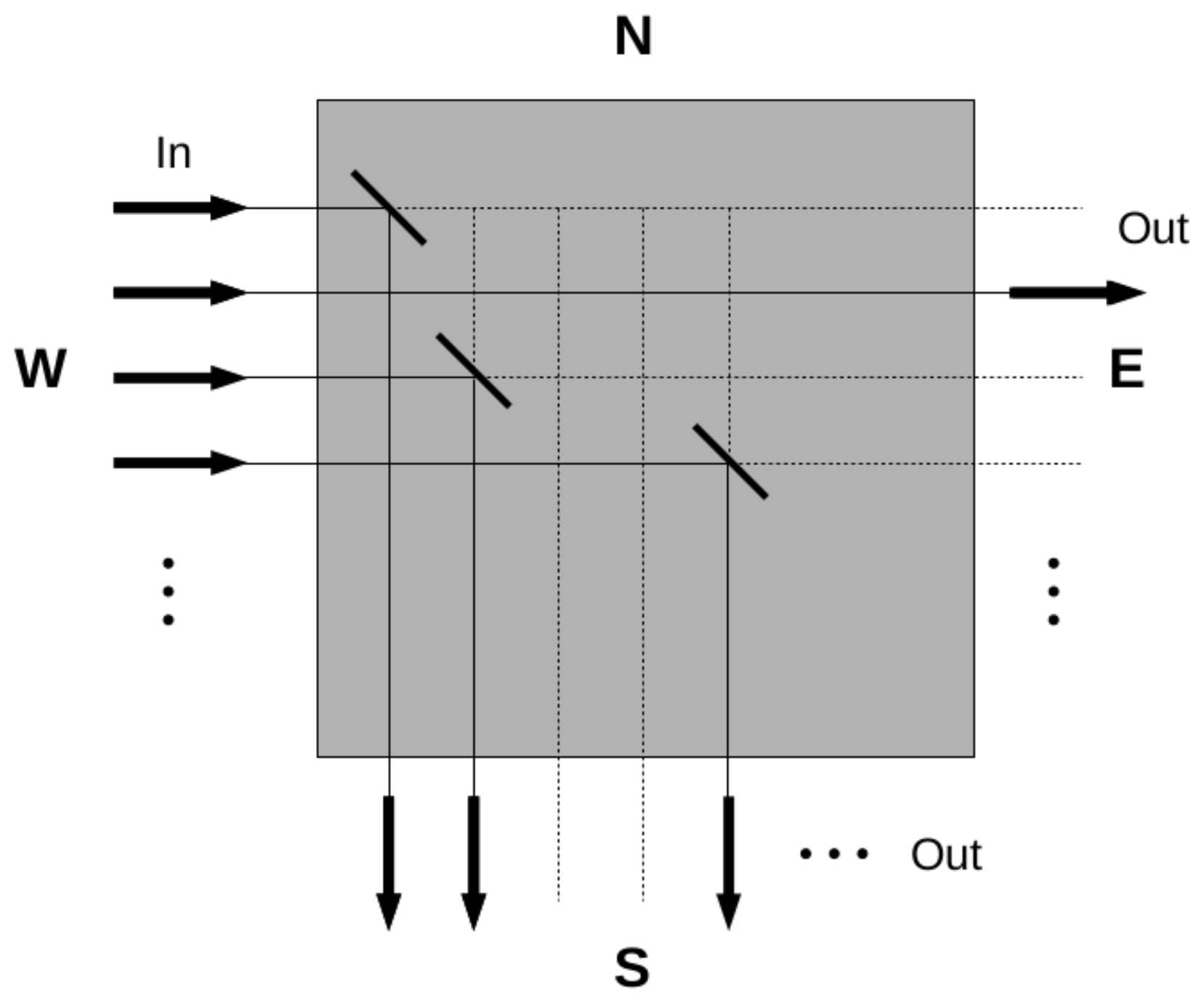
The current state-of-the-art optical switching technology is based on micro-electro-mechanical systems (MEMSs) where an array of micro mirrors is oriented to reflect the incident light toward specific output ports [7,8,9]. The first generation of these MEMSs was designed so the light is propagating along the plane of the devices, e.g., west–east. When a mirror initially laying flat on the surface was raised up, it intercepted the beam and reflected it at in the north–south direction. Since the layout of this switch was within a plane, this configuration was named two-dimensional (2D) MEMS. A schematic representation is presented in Figure 1. The binary orientation of the mobile mirrors, flat or raised, simplified the electronic control. However, to obtain a strictly non-blocking switch with such an architecture, number of mirrors are needed, with N being the number of accessible ports [10]. This quadratic increase of the number of active mirrors limited its adoption for large numbers of ports.
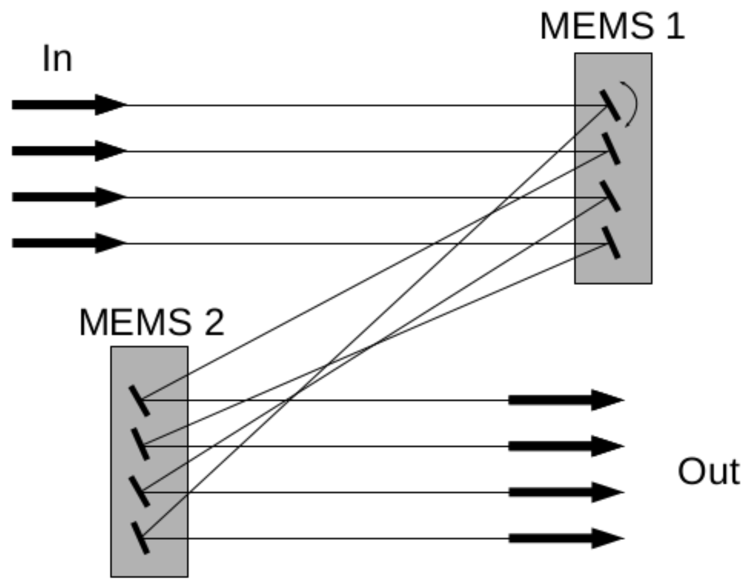
The second generation of MEMS switches takes advantage of reflection away from the plane of the device. Dubbed three-dimensional (3D) MEMSs, they are composed of micro mirrors lying in the plane of the substrate and mounted on a gimbaled support. The orientation of the mirrors can be continuously adjusted over a range of tip and tilt angles so the reflection of the incoming light is directed to a specific output port. To minimize the overall system losses, it is critical to ensure that the reflected light is within the acceptance angle of the fiber at the output port requiring that the 3D MEMSs are used in pairs. The first 3D MEMS reflects the light at an angle toward the second unit, which corrects that angle to align the beam orthogonal to the output port fiber. A schematic representation of this configuration is presented in Figure 2. Although the control electronic of such an analog MEMS is more complex than for a digital system, the advantage of that configuration is that a non-blocking configuration for N ports can be obtained with only mirrors. This allows for building a switch with a much larger number of ports [11,12].
The speed at which the mirrors can be repositioned in a reflection-based optical switch is in the order of a few milliseconds. This speed depends on the mirror mass m: the larger the mirror, the more time it takes to re-orient it. This can be understood by comparing the mirror to an harmonic oscillator whose frequency is given by , with k the spring constant. In this configuration, the mass of the mirror is proportional to its area which is dictated by the beam diameter.
The 3D MEMS mirrors have a diameter of about 500 microns. Smaller beam diameter and mirror sizes could be achieved with faster optics (shorter focal length), but that requires larger angular amplitude from the mirror. In these conditions, the hinge mechanism is subject to higher mechanical stress and has an increased failure rate. In the 3D MEMS design, the system imposes a trade-off between the mirror’s angular amplitude and its mass, which translates into a trade-off between the number of ports accessible by the switch and its reconfiguration speed [13]. It is worth noting that the mirror size is also limited by the energy density of the beam, and the damage threshold of the mirror coating.
Breaking the millisecond reconfiguration speed limit requires the introduction of another paradigm: instead of using reflection from a mirror, it is possible to use diffraction from several elements.
2. Diffraction-Based Optical Switching
To reduce the MEMS mirror weight, the size needs to decrease. However, with tens of microns or less in diameter, using the mirrors as reflectors becomes inefficient. First, the power density is too large, and second, the scattering from the edges of the mirror induces loss. One solution is to distribute the incident beam over several mirrors, and take advantage of the diffraction by using a computer generated hologram. In this embodiment, the MEMS device does not need to have mirrors that change orientation as is the case for 3D MEMS, but pixels that modulate either the amplitude or the phase of the incident beam.
The diffraction patterns are computed using a Fraunhofer diffraction integral Equation (1) and a Gerchberg-Saxton type iterative algorithm [14]
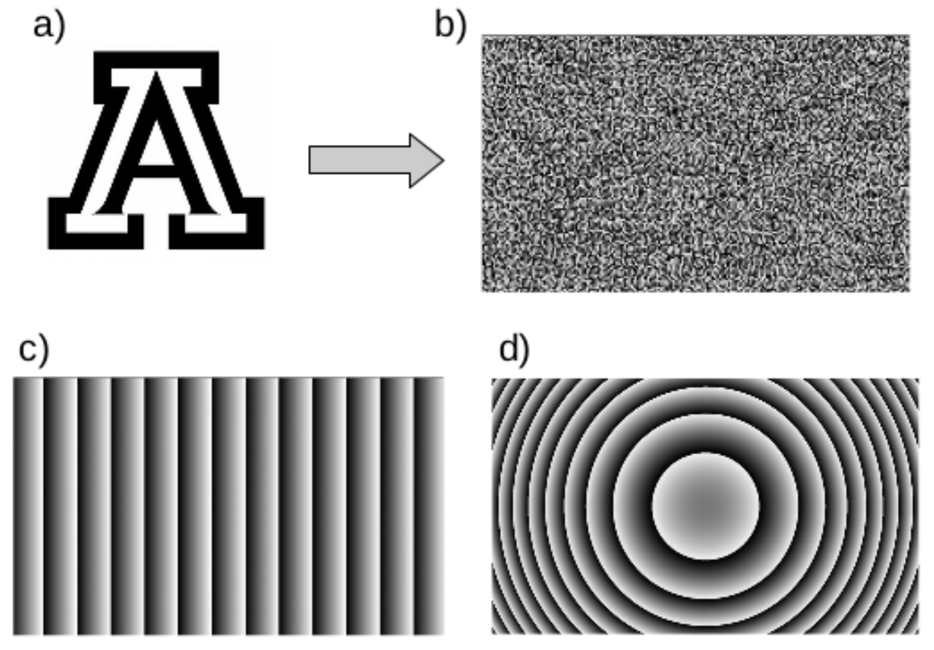
Example of diffraction patterns are presented in Figure 3.
If the diffraction pattern is a grating with frequency , the beam is diffracted at an angle given by the grating equation:
where is the angle of incidence of the beam, m the order of diffraction, is the wavelength of the light.
In this approach, changing the output port of the switch can be done by changing the spatial frequency of the grating displayed by the Spatial Light Modulator (SLM). A decomposition of all possible gratings that could be displayed by the SLM into its Fourier components demonstrates that there could be as many output ports as the number of pixels on the SLM.
If more than one input port is needed for the switch, the clear aperture of the SLM can be divided into several sub-apertures, each diffracting the beam coming from a different input port. It has to be noted that in the case of a volume hologram, angular multiplexing can be used to diffract multiple inputs to multiple outputs without crosstalk. However, this type of thick volume hologram cannot yet be realized with the SLM.
By using diffraction instead of reflection, other optical functions can be added to the SLM. Examples of such functions are focalization by a Fresnel or Gabor zone plate, aberration correction for coma or astigmatism due to the off-axis diffraction of the beam, variation of the focal length to accommodate a curved focal plane. Another advantage of a diffraction-based optical switch is the possibility for multicasting and signal aggregation. Multicasting happens when the signal from a single input port is distributed over multiple output ports, and aggregation happens when the signal from multiple input ports is combined to a single output port.
To demonstrate the potential of an holographic-based optical switch, we used a Texas Instruments DLP (Digital Light Processing) in our initial prototype [15,16]. The DLP is a MEMS where the mirrors can be tilted in two different directions. In the most popular versions (0.7 XGA (Extended Graphics Array), and 0.95 1080p) the direction of the tilt is . With such a binary mirror operation, the DLP cannot modulate the phase of the light, but it is capable of displaying binary amplitude diffraction patterns that are capable of redirecting the beam. For binary amplitude modulation, scalar theory of diffraction shows that the maximum diffraction efficiency that can be achieved is 10% [14]. However, the advantage of using the DLP is that it updates the diffraction pattern at rates of up to 32,552 Hz.
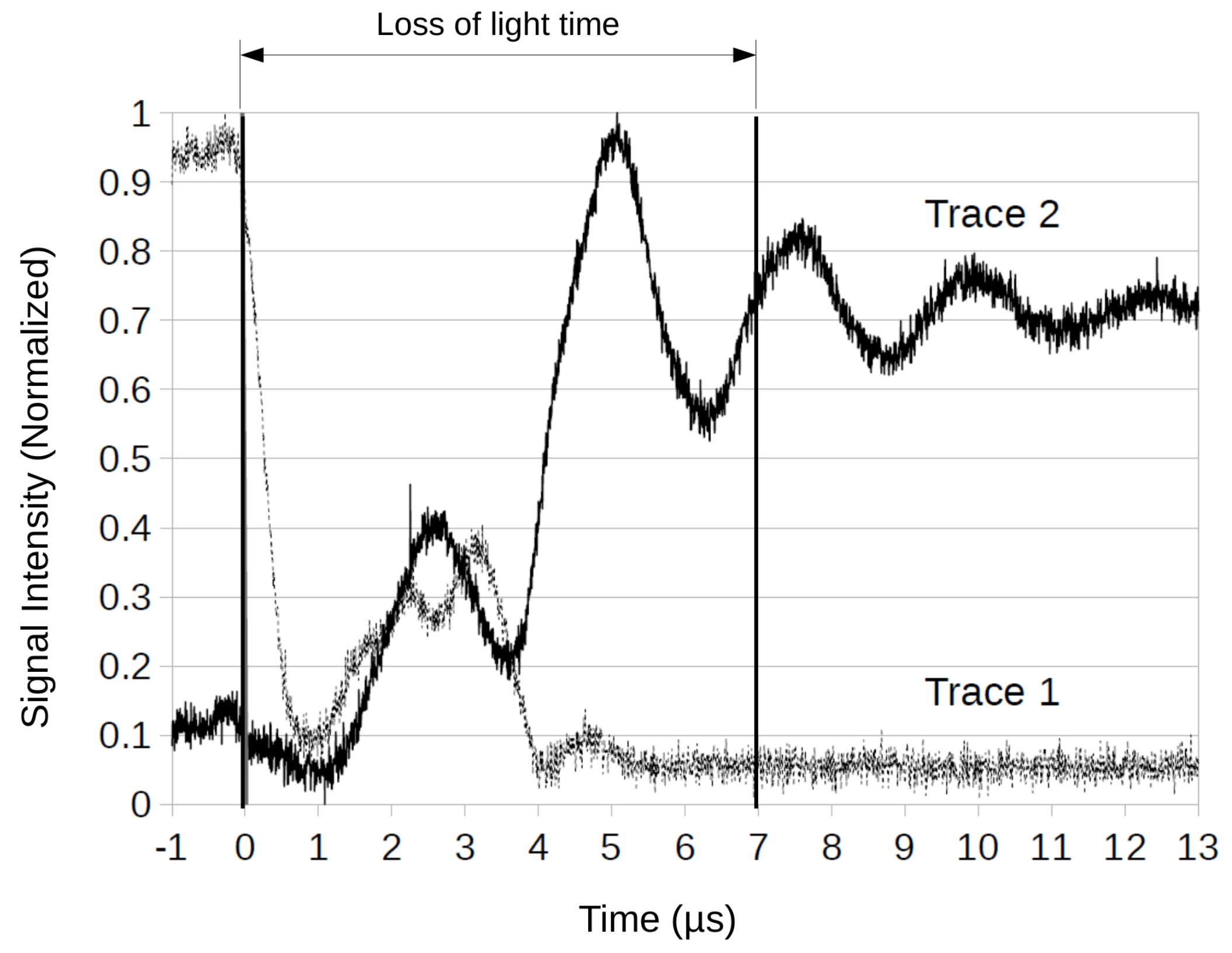
We measured the loss-of-light time for the DLP Discovery 4100 Chipset. The loss-of-light time is defined as the interval during which the communication is interrupted between the emitter and receptor due to the reconfiguration of the mirror. As presented in Figure 4, the loss-of-light time is only s before the signal is reacquired, and could further be reduced to s if −2 dB loss is acceptable by the communication link.
The fast reconfiguration time has several advantages for next generation data center architectures. In their implementation, Ghobadi et al. [17] used the diffractive switch technology to interconnect every pair of racks and developed a specific topology and routing methods to exploit the capabilities of the switch. In their experiments and simulations using realistic data center workloads, they showed that, compared to the conventional folded-Clos interconnect, this approach can improve mean flow completion time by 30–95% and reduce the capital cost by 25–40%.
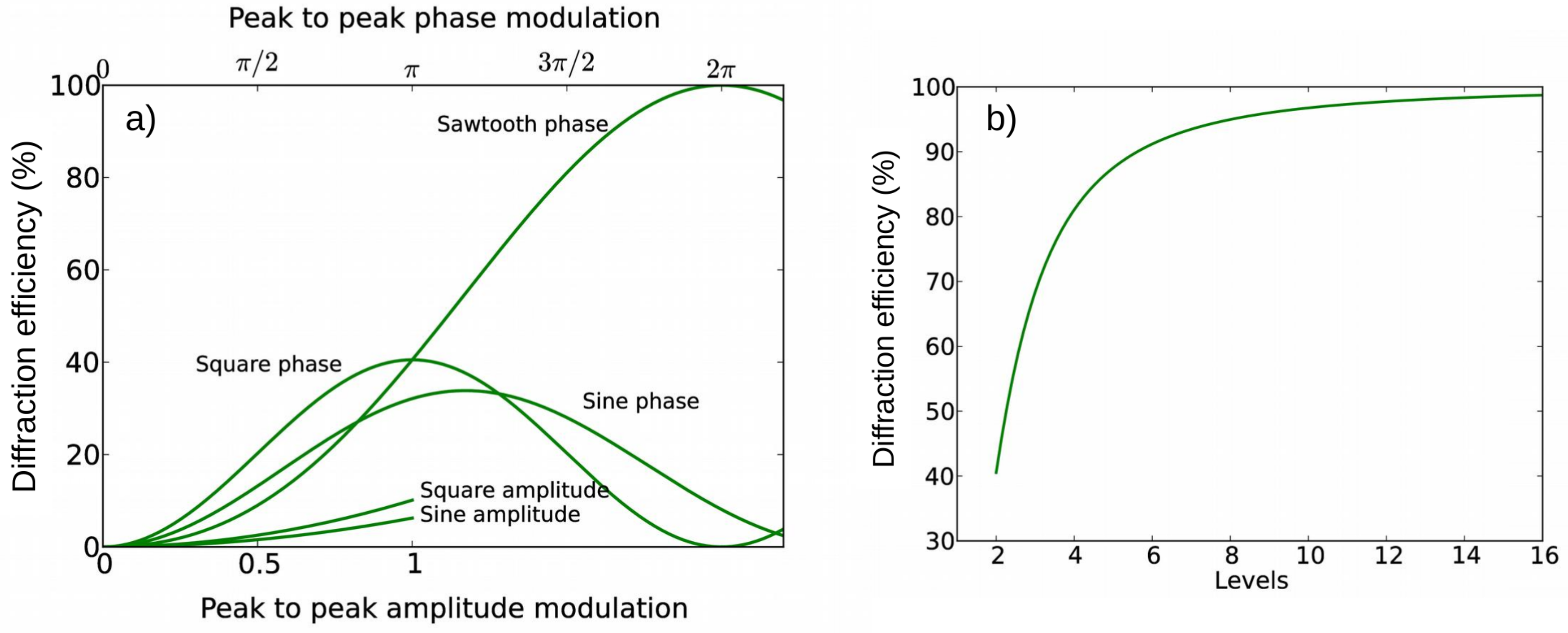
In another prototype of the holographic switch, we replaced the DLP element by an LCoS (Liquid Crystal on Silicon) SLM (Holoeye PLUTO-TELCO-013). The goal of using an LCoS instead of a DLP is that the LCoS SLM can achieve a much higher diffraction efficiency. Figure 5 shows the computation for the diffraction efficiency according to the type of modulation forming the hologram. We can see that square wave transmission holograms, which are the type reproduced by the DLP, can only achieve 10.1%. The other 89.9% of the signal is lost in other diffracted orders.
LCoS SLMs are capable of generating phase modulation holograms which can achieve up to 100% diffraction efficiency for a sawtooth function. However, the driver electronics in the LCoS system are not designed to represent a continuous function but a discrete set of values, most frequently 8 bits, or 256 phase value. In this case, the efficiency according to the number of levels N is given by:
Equation (3) is presented in the right panel of Figure 5, starting at 40.5% for a binary square phase pattern (identical to the value computed in the left panel), and increasing asymptotically toward 100% as the number of levels increases toward infinity. In practice, an LCoS device will also suffer additional losses due to the reflectivity of the mirrors, and fill factor.
If efficiency is the main advantage of LCoS technology, its main limitation is the reconfiguration speed. Due to the viscoelastic coefficient of the liquid crystal, the maximum refresh rate is only a few hundred hertz (180 Hz in case of the Holoeye PLUTO). This slow refresh rate, compared to the tens of kHz achieved by the DLP, limits the switch reconfiguration time in the millisecond regime, and does not provide a competitive advantage over the 3D MEMS.
It has to be pointed out that research is still ongoing to increase the speed of LCoS SLM. A 100 s refresh rate can be obtained with ferroelectrics liquid crystals but they offer only binary phase modulation at this speed [18]. Blue phase chiral nematic liquid crystal can be driven at kHz frequency but only achieve modulation at relatively high voltage (tens of volts), and this phase is only stable over a small temperature range [19]. Some devices exploiting the flexoelectric-optic effect in chiral nematic liquid crystal has shown sub-millisecond response time [20]. Unfortunately, no reliable sub-millisecond LCoS SLM is commercially available at this time.
Nevertheless, to demonstrate the potential of holographic switching, we used an LCoS SLM to confirm the benefit of a phase modulator over amplitude modulator. Using the LCoS SLM, we built a prototype to showcase two important aspects of a diffraction-based optical switch: the ability to access a large number of ports, and the compatibility of the switch with industry standard phase shift keying for the signal modulation.
As discussed in an earlier section, the number of individual locations potentially addressable with an SLM using a diffraction grating is identical to the number of pixels. However, this conclusion is using the Rayleigh criterion with −3 dB cross talk between the points in the hologram plane. For telecommunication applications, crosstalk between ports must be less than −33 dB to minimize the introduction of unwanted noise in future amplification steps. For a fiber-based diffraction switch, the signal injected to a neighbor port depends on the spatial extent of the signal over that port, and the insertion loss due to the fiber acceptance angle. To reduce the spatial extent of the diffracted beam to a minimum, we used a blazed zone plate lens pattern, as presented in Figure 3d, to diffract the incident beam. This has the advantage of maximizing the efficiency in the +1 order, and generates a diffraction limited spot at the location of the output fiber. By shifting the zone plate on the SLM, the diffracted beam is shifted by the same amount in the hologram plane (in a 2f configuration). The minimum amount of lateral displacement between locations is of course 1 pixel, which in our case was m. However, with only m separation between neighboring locations, the crosstalk was above −33 dB, and single mode fibers could not be packed that closely. Measurement showed that output ports need to be separated by at least m (13 pixels) to reduce the crosstalk below −33 dB. This measurement has an important implication for the number of ports accessible with a single SLM. Considering a 1080p pixel count, the number of output ports is . Using 4K cinema resolution, the number of output ports climbs up to over 52,000.
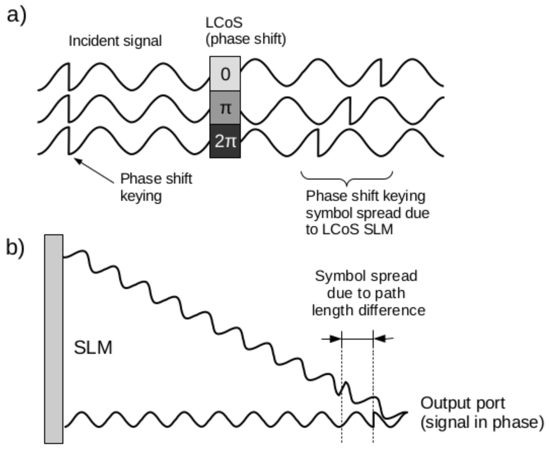
Modern telecommunications networks are increasingly employing signal modulation techniques to increase transmission bandwidths. For the diffraction switch to be adopted, it must be compatible with the phase shift keying (PSK) common modulation technique. The PSK technique relies on phase delay of the wave modulation, but the diffraction switch is also modifying the phase of the incoming light beam. The LCoS SLM can modify the phase by a maximum of , as shown in the top panel of Figure 6. However, the difference in path length due to the propagation from different regions of the SLM induces further phase shift. At the output port location, the beams coming from different location on the SLM have the same relative phase, however they experience an absolute phase shift of a multiple of as shown in Figure 6b.
Fortunately, the light frequency and the signal modulation frequency are different enough to allow for the introduction of some phase shift by the holographic switch. For (central C band wavelength), the light frequency is , when a signal modulation at e.g., 25 Gbaud/s has a frequency of . The ratio between these two frequencies gives the number of light periods between two symbols: . If the diffraction switch introduces less than this number of shifts, there will be a region where a stable signal can be detected. The exact amplitude of phase shift accepted by the transmission line depends of the exact configuration of the line and should be measured for a specific configuration to determine the bit error rate at an increasing modulation rate.
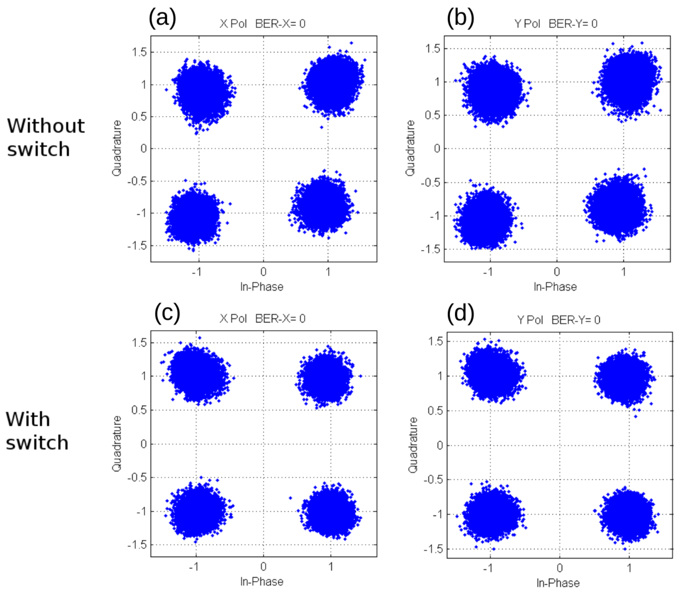
We tested our LCoS-based optical switch with a QPSK (Quadrature Phase Shift Keying) signal and examined the clustering of the demodulated signal with and without the switch in the transmission line. The constellation diagrams for both x and y incident polarizations are presented in Figure 7. No signal degradation was observed for the diffraction by a zone plate containing up to 600 rings, i.e., phase shift.
3. Phase Modulation MEMS
In the previous section, we explained how we used the Texas Instruments DLP to demonstrate the concept of holographic optical switches, and why the diffraction efficiency was limited to 10% due to the amplitude modulation of the light field. We also describe how low loss switching can be achieved with phase modulator array such as LCoS. However, LCoS have a slow response time (∼milliseconds) due to the viscoelasticity of the medium.
The answer to both these problems would be a MEMS-based SLM array with pure phase modulation. The individual pixels of this system would be based on micro-reflectors as in the case of the DLP, but instead of modulating the amplitude of the incident light, they would affect the phase, as in the case of the LCoS. By merging these two elements, the phase modulation MEMS offers both high diffraction efficiency (see Figure 5), and fast switching time (∼ microsecond). It also has the added benefit of a sharper phase transition than LCoS because there is no voltage leakage between the pixels.
Recently, we have reported a new spatial light phase modulator array with MEMS piston mirrors [21]. Phase modulation is achieved by electrostatically pulling down the mirrors by a fraction of the wavelength (from 0 to ), which affects the beam path length (from 0 to ). A schematic representation the cross section of this system is presented in Figure 8a.
To reduce the mirror mass and increase the actuation speed, we used a novel high-contrast grating (HCG) [22]. The HCG mirrors consist of a thin layer of silicon (∼300 nm) structured with beam and void to form a sub-wavelength grating as presented in Figure 8b. These pixels have a high reflectivity over a broad optical frequency band (from 1300 nm to 2300 nm in our example), which is not the case for the distributed Bragg reflector. We have demonstrated phase modulator array with a pitch of 22 m. This array is capable of optical beam steering from to with microsecond response time.
To increase the steering angle, the pixel size and the pitch of the array need to be further reduced. Indeed, the maximum scan angle is related to the pitch of the phase structure by the Bragg’s equation:
where is the optical wavelength.
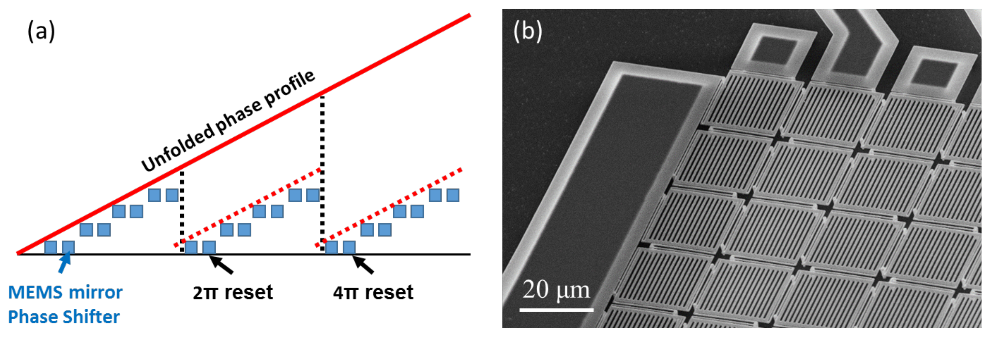
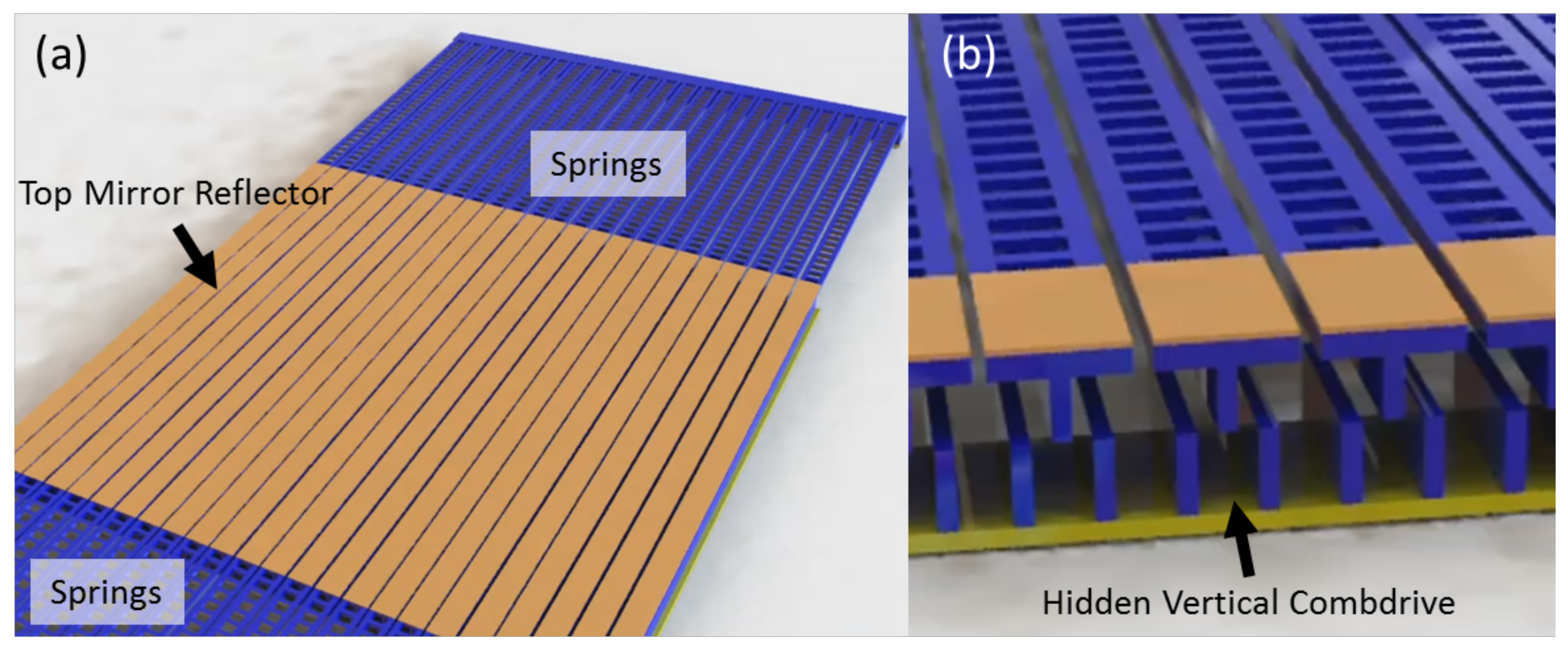
However, reducing the pixel and array pitch size puts significant constraints on the actuation mechanism and a different approach is needed. In our latest phase MEMS embodiment presented in Figure 9, we used a staggered vertical combdrive (SVC) actuator with submicrometer fingers and spacing (300 nm). The combdrive actuator has been chosen for its large interaction length with the stator which increases the pulling force [23]. Compared with other actuator designs such as parallel plate [24], the SVC design minimizes the fringe effects of the electrical fields during actuation, and therefore allows for denser arrangement of the pixels in parallel without significant crosstalk. Thus, the SVC hidden underneath the mirror can increase the fill factor of the array. Top and bottom parts of the column are used as springs to ensure adequate flexibility and travel of the element. The central part of the column is coated with metal to act as a high reflective mirror.
This column configuration bears a few similarities with the grating light valve developed in the 1990s at Stanford University [25]. However, in our case, the height of the reflector elements can be modulated to various levels. This added capability allows for higher diffraction efficiency and the selection of the diffraction angle, which was not possible with the binary light valve.
We were able to fabricate a one-dimensional (1-D) phase modulator array with a pitch of only m [26]. This array is capable of steering light over at 1550 nm wavelength, which is 10 times larger than with the square pixels configuration presented in Figure 8. The mirrors of the array are tethered to the anchors through a pair of springs. Each mirror is m wide and m long, and the pitch is m, resulting in a 87.5% fill-factor. The mirrors and the top combs are grounded while the bottom combs are individually addressed to produce the desired phase profiles such as a highly efficient blazed grating (see Figure 5). The measured resonant frequency of this MEMS is 310 kHz, which corresponds to a switching time of a few microseconds. Compared with LCoS and binary MEMS devices such as the DLP, this new MEMS benefits from a fast response time (microseconds), a large field of view (tens of degrees), and low loss (−1.4 dB, including fill factor and reflection losses). It is also wavelength-, polarization- and modulation-agnostic. All these properties make the piston mode MEMS array an attractive choice for optical switch applications.
4. Conclusions
Optical switch can play an important role in data communication by replacing electronic circuit switching, reducing the energy consumption of data centers, and be agnostic to both the data rate and modulation format. For this transformation to truly happen, the switching speed of the current 3D MEMS technology needs to be increased to at least the range. A potential solution is to reduce the size of the micro mirrors, and use the MEMS as a diffractive element. For this configuration to be efficient, the MEMS element should modulate the phase of the light. Three critical steps in this direction have been demonstrated so far: first, the use of the Texas Instruments DLP to prove the concept of diffractive switching and assess the switching speed; second, the use of LCoS SLM technology to determine the ability of the phase optical switch to meet existing telecommunication infrastructure requirements for efficiency, cross talk, and encoding format support; and third, the development of prototypes of optical phase array MEMS to establish the architecture.
All the experimental measurements so far have demonstrated that the diffraction-based phase modulation MEMS approach is a viable solution for high speed, low loss, and low power consumption optical switching.
Acknowledgments
The authors would like to thank Dr. Arkady Bablumian and Richard Rankin for discussion on diffractive switch architecture, as well as Weiyang Mo for the access to the NSF TOAN lab testing facility at the University of Arizona. The authors acknowledge support from the National Science Foundation through CIAN NSF ERC under grant EEC-0812072, and PFI:AIR-TT 1640329, as well as from the Department of Energy under grant SBIR DE-SC0015178.
Author Contributions
P.-A.B. did the experiment with the DLP and LCoS, and wrote Section 1, Section 2, and Section 4. L.L. did the LCoS QPSK experiment. Y.W. was involved in the phase modulation MEMS manufacturing and testing, and wrote Section 3. M.C.W. was involved in the phase modulation MEMS manufacturing and testing.
Conflicts of Interest
The authors declare no conflict of interest.
Abbreviations
The following abbreviations are used in this manuscript:
| DLP | Digital Light Processing |
| DMD | Digital Micromirror Device |
| HCG | High-Contrast Grating |
| LCoS | Liquid Crystal on Silicon |
| MEMS | Micro Electro Mechanical System |
| QPSK | Quadrature Phase Shift Keying |
| SLM | Spatial Light Modulator |
| SRG | Surface Relief Grating |
| SVC | Staggered Vertical Combdrive |
References
- El-Bawab, T.S. Optical Switching, 1st ed.; Springer Science & Business Media: Berlin/Heidelberg, Germany, 2006. [Google Scholar]
- Ma, X.; Kuo, G. Optical switching technology comparison: Optical MEMS vs. other technologies. IEEE Commun. Mag. 2003, 41, 16–24. [Google Scholar]
- CISCO. Cisco Global Cloud Index: Forecast and Methodology, 2015–2020; Technical Report; CISCO: San Jose, CA, USA, 2016. [Google Scholar]
- Natural Resources Defense Council (NRDC). America’s Data Centers Consuming and Wasting Growing Amounts of Energy; Technical Report; NRDC: New York, NY, USA, 2014. [Google Scholar]
- Thibodeau, P. Data Centers Are the New Polluters. Computerworld. Available online: http://www.computerworld.com/article/2598562/data-center/data-centers-are-the-new-polluters.html (accessed on 12 April 2017).
- Lentine, A. Challenges for optical interconnect for beyond Moore’s law computing. In Proceedings of the IEEE International Conference on Rebooting Computing (ICRC), San Diego, CA, USA, 17–19 October 2016. [Google Scholar]
- Yeow, T.W.; Law, K.E.; Goldenberg, A. MEMS optical switches. IEEE Commun. Mag. 2001, 39, 158–163. [Google Scholar] [CrossRef]
- De Dobbelaere, P.; Falta, K.; Gloeckner, S.; Patra, S. Digital MEMS for optical switching. IEEE Commun. Mag. 2002, 40, 88–95. [Google Scholar] [CrossRef]
- Chu, P.B.; Lee, S.S.; Park, S. MEMS: The path to large optical crossconnects. IEEE Commun. Mag. 2002, 40, 80–87. [Google Scholar] [CrossRef]
- Yeow, T.W.; Law, K.E.; Goldenberg, A.A. Micromachined L-switching matrix. In Proceedings of the IEEE International Conference on Communications (ICC 2002), New York, NY, USA, 28 April–2 May 2002; Volume 5, pp. 2848–2854. [Google Scholar]
- Kim, J.; Nuzman, C.; Kumar, B.; Lieuwen, D.; Kraus, J.; Weiss, A.; Lichtenwalner, C.; Papazian, A.; Frahm, R.; Basavanhally, N.; et al. 1100 × 1100 port MEMS-based optical crossconnect with 4-dB maximum loss. IEEE Photonics Technol. Lett. 2003, 15, 1537–1539. [Google Scholar] [CrossRef]
- Mizukami, M.; Yamaguchi, J.; Nemoto, N.; Kawajiri, Y.; Hirata, H.; Uchiyama, S.; Makihara, M.; Sakata, T.; Shimoyama, N.; Oda, K. 128 × 128 three-dimensional MEMS optical switch module with simultaneous optical path connection for optical cross-connect systems. Appl. Opt. 2011, 50, 4037–4041. [Google Scholar] [CrossRef] [PubMed]
- Mellette, W.M.; Ford, J.E. Scaling Limits of MEMS Beam-Steering Switches for Data Center Networks. J. Lightwave Technol. 2015, 33, 3308–3318. [Google Scholar] [CrossRef]
- Blanche, P.A. Field Guide to Holography; SPIE Press Book: Bellingham, WA, USA, 2014; Volume FG31. [Google Scholar]
- Lynn, B.; Blanche, P.A.; Miles, A.; Wissinger, J.; Carothers, D.; LaComb, L.; Norwood, R.A.; Peyghambarian, N. Design and Preliminary Implementation of an N × N Diffractive All-Optical Fiber Optic Switch. J. Lightwave Technol. 2013, 31, 4016–4021. [Google Scholar] [CrossRef]
- Miles, A.; Lynn, B.; Blanche, P.A.; Wissinger, J.; Carothers, D.; LaComb, L., Jr.; Norwood, R.; Peyghambarian, N. 7 × 7 DMD-based diffractive fiber switch at 1550 nm. Opt. Commun. 2015, 334, 41–45. [Google Scholar] [CrossRef]
- Ghobadi, M.; Mahajan, R.; Phanishayee, A.; Devanur, N.; Kulkarni, J.; Ranade, G.; Blanche, P.A.; Rastegarfar, H.; Glick, M.; Kilper, D. Projector: Agile reconfigurable data center interconnect. In Proceedings of the 2016 Conference on ACM SIGCOMM 2016 Conference, Florianópolis, Brazil, 22–26 August 2016; pp. 216–229. [Google Scholar]
- Fracasso, B.; Ambs, P.; de la Tocnaye, J.D.B. Recording reconfigurable binary computer-generated holograms on bistable optically addressed ferroelectric liquid-crystal spatial light modulators. Opt. Lett. 1990, 15, 1473–1475. [Google Scholar] [CrossRef] [PubMed]
- Yan, J.; Xing, Y.; Guo, Z.; Li, Q. Low voltage and high resolution phase modulator based on blue phase liquid crystals with external compact optical system. Opt. Express 2015, 23, 15256–15264. [Google Scholar] [CrossRef] [PubMed]
- Chen, J.; Morris, S.M.; Wilkinson, T.D.; Freeman, J.P.; Coles, H.J. High speed liquid crystal over silicon display based on the flexoelectro-optic effect. Opt. Express 2009, 17, 7130–7137. [Google Scholar] [CrossRef] [PubMed]
- Yoo, B.W.; Megens, M.; Sun, T.; Yang, W.; Chang-Hasnain, C.J.; Horsley, D.A.; Wu, M.C. A 32 × 32 optical phased array using polysilicon sub-wavelength high-contrast-grating mirrors. Opt. Express 2014, 22, 19029–19039. [Google Scholar] [CrossRef] [PubMed]
- Yoo, B.W.; Megens, M.; Chan, T.; Sun, T.; Yang, W.; Chang-Hasnain, C.J.; Horsley, D.A.; Wu, M.C. Optical phased array using high contrast gratings for two dimensional beamforming and beamsteering. Opt. Express 2013, 21, 12238–12248. [Google Scholar] [CrossRef] [PubMed]
- Hah, D.; Patterson, P.R.; Nguyen, H.D.; Toshiyoshi, H.; Wu, M.C. Theory and experiments of angular vertical comb-drive actuators for scanning micromirrors. IEEE J. Sel. Top. Quantum Electron. 2004, 10, 505–513. [Google Scholar] [CrossRef]
- Payne, A.; Myatt, G.; Hunter, J.; Yeung, M.; Lu, J.; Beach, G.; Volchegursky, A.; Eng, L. An 8192-channel grating light valve for ultra-violet direct write lithography. In Proceedings of the 2012 International Conference on Optical MEMS and Nanophotonics (OMN), Banff, AB, Canada, 6–9 August 2012; pp. 188–189. [Google Scholar]
- Solgaard, O. Integrated Semiconductor Light Modulators for Fiber-Optic and Display Applications. Ph.D. Thesis, Stanford University, Stanford, CA, USA, 1992. [Google Scholar]
- Wang, Y.; Wu, M.C. Micromirror based optical phased array for wide-angle beamsteering. In Proceedings of the 2017 IEEE 30th International Conference on Micro Electro Mechanical Systems (MEMS), Las Vegas, NV, USA, 22–26 January 2017; pp. 897–900. [Google Scholar]
Figure 1.
Schematic representation of a two-dimensional micro-electro-mechanical system (2D MEMS).

Figure 2.
Schematic representation of a cross section of a three-dimensional (3D) MEMS in butterfly configuration.
Figure 2.
Schematic representation of a cross section of a three-dimensional (3D) MEMS in butterfly configuration.

Figure 3.
Example of diffraction patterns. (a) Original image; (b) Diffraction pattern obtained by a Gerchberg–Saxton algorithm; (c) Blazed grating; (d) Blazed zone plate.
Figure 3.
Example of diffraction patterns. (a) Original image; (b) Diffraction pattern obtained by a Gerchberg–Saxton algorithm; (c) Blazed grating; (d) Blazed zone plate.

Figure 4.
Measurement of the loss-of-light time due to the update of the diffractive pattern by the DLP (Digital Light Processing). Trace 1 and 2 are signal diffracted toward photo detector 1 and 2.
Figure 4.
Measurement of the loss-of-light time due to the update of the diffractive pattern by the DLP (Digital Light Processing). Trace 1 and 2 are signal diffracted toward photo detector 1 and 2.

Figure 5.
Diffraction efficiency according to (a) the type of modulation; (b) the number of phase levels addressable by the diffracting device between 0 and .
Figure 5.
Diffraction efficiency according to (a) the type of modulation; (b) the number of phase levels addressable by the diffracting device between 0 and .

Figure 6.
Phase shifting of the phase shift keying (PSK) symbol induced by (a) the LCoS SLM (Liquid Crystal on Silicon Spatial Light Modulator); (b) the difference in path length.
Figure 6.
Phase shifting of the phase shift keying (PSK) symbol induced by (a) the LCoS SLM (Liquid Crystal on Silicon Spatial Light Modulator); (b) the difference in path length.

Figure 7.
Constellation diagrams of a 25 Gbaud/s signal. (a) no switch, x-polarization; (b) no switch, y-polarization; (c) with switch, x-polarization; (d) with switch, y-polarization. , phase pattern: 600 rings zone plate.
Figure 7.
Constellation diagrams of a 25 Gbaud/s signal. (a) no switch, x-polarization; (b) no switch, y-polarization; (c) with switch, x-polarization; (d) with switch, y-polarization. , phase pattern: 600 rings zone plate.

Figure 8.
(a) Cross section schematic of the phase modulation by a diffractive MEMS micromirror array. The phase modulation is achieved by controlling individual mirror height to match the desired phase profile modulo ; (b) Scanning electron micrograph (SEM) of a phase modulator array with high-contrast-grating (HCG) mirrors.

Figure 9.
Illustration of the fine pitch diffraction MEMS phase modulation array. (a) Isometric view of the diffractive MEMS phase modulation array; (b) Cross-sectional view of the device showing the hidden vertical combdrive structure.
Figure 9.
Illustration of the fine pitch diffraction MEMS phase modulation array. (a) Isometric view of the diffractive MEMS phase modulation array; (b) Cross-sectional view of the device showing the hidden vertical combdrive structure.

© 2017 by the authors. Licensee MDPI, Basel, Switzerland. This article is an open access article distributed under the terms and conditions of the Creative Commons Attribution (CC BY) license (http://creativecommons.org/licenses/by/4.0/).
Share and Cite
MDPI and ACS Style
Blanche, P.-A.; LaComb, L.; Wang, Y.; Wu, M.C. Diffraction-Based Optical Switching with MEMS. Appl. Sci. 2017, 7, 411. https://0-doi-org.brum.beds.ac.uk/10.3390/app7040411
AMA Style
Blanche P-A, LaComb L, Wang Y, Wu MC. Diffraction-Based Optical Switching with MEMS. Applied Sciences. 2017; 7(4):411. https://0-doi-org.brum.beds.ac.uk/10.3390/app7040411
Chicago/Turabian StyleBlanche, Pierre-Alexandre, Lloyd LaComb, Youmin Wang, and Ming C. Wu. 2017. "Diffraction-Based Optical Switching with MEMS" Applied Sciences 7, no. 4: 411. https://0-doi-org.brum.beds.ac.uk/10.3390/app7040411
Note that from the first issue of 2016, this journal uses article numbers instead of page numbers. See further details here.