A Dual Stage Low Power Converter Driving for Piezoelectric Actuator Applied in Micro Mobile Robot

College of Instrumentation & Electrical Engineering, Key Laboratory of Geo-exploration Instruments, Ministry of Education of China, Jilin University, Chang Chun 130026, China
*
Author to whom correspondence should be addressed.
Appl. Sci. 2018, 8(9), 1666; https://0-doi-org.brum.beds.ac.uk/10.3390/app8091666
Submission received: 11 August 2018
/
Revised: 11 September 2018
/
Accepted: 11 September 2018
/
Published: 15 September 2018
(This article belongs to the Special Issue Advanced Mobile Robotics)
Abstract
:Piezoelectric actuators are widely utilized to convert electrical energy into mechanical strain with considerable potential in micro mobile robot applications. However, the use of Pb-based Lanthanumdoped Zirconate Titanates (PZTs) leads to two difficulties in drive circuit design, namely, high voltage step-up ratio and high energy conversion efficiency. When some devices driven by piezoelectric actuators are used in emerging technologies, such as micro mobile robot, to perform special tasks, low mass, high energy density, and high conversion efficiency are strategically important. When these demands are considered, conventional drive circuits exhibit the disadvantages of being too bulky and inefficient for low mass applications. To overcome the aforementioned drawbacks, and to address the need for a piezoelectric bimorph actuator, this work proposed a high step-up ratio flyback converter cascaded with a bidirectional half-bridge stage controlled, via a pulse width modulation strategy, and a novel control method. Simulations and experiments were conducted to verify the ability of the proposed converter to drive a 100 V-input piezoelectric bimorph actuator using a prototype 108 mg (excluding printed circuit board mass), 169 (13 × 13) mm2, and 500 mW converter.
1. Introduction
Microrobots represent a new type of bionic robots inspired by insects to achieve ultracompact size, high mobility, and remote controllability; these robots have many applications, including those in bioengineering, disaster relief, microsurgery, and surveillance [1,2,3]. Among microrobots, micro mobile robots (MMRs) are widely used in environmental monitoring, rescue operations, and agricultural production, due to their high energy efficiency and high mobility. If the energy conversion efficiency of the frame, including the actuator, power circuit design, and mechanical transmission for stroke amplification can be improved, then the application prospects of such robots will be extended.
As a displacement device, actuators are widely used in many types of micromechanical devices like walking, swimming, jumping robots and so on [4,5,6]. Among them, especially, the actuator plays a critical role in obtaining sufficient lift force. Prior works on actuators in MMR applications include studies on an electromagnetic actuator, a shape-memory alloy actuator, an electrostatic actuator, and a dielectric elastomer actuator [7,8,9,10]. However, the disadvantages of low response rate, small mechanical displacement, and low conversion efficiency limit their applications to MMRs.
The breakthrough in piezoelectric bimorph actuators with high bandwidth and high power density achieved by Wood et al. in a multi-segmented centipede robot. Meanwhile, Wood et al. considered a complete fabrication solution for actuators, links, flexures, integrated wiring, and structural elements using high-performance materials; they then developed a highly efficient transmission link for a specific device [11]. However, a power electronic unit connected to a piezoelectric actuator faces two major challenges [12]. Firstly, high voltages within the range of 100–120 V are required to generate sufficient force and displacement. Most energy sources compatible with the weight budget of MMR applications have output voltages of 3–5 V. Consequently, power interface circuits require high step-up ratio. Secondly, a piezoelectric actuator provides only a fraction of the input energy required for effective displacement. In addition, prior work in dynamic performance analysis of piezoelectric actuator include Nabawy et al., which demonstrated comprehensive analytical model of both unimorph and bimorph structure [13,14]. Different drive frequencies and signal amplitudes can affect the electromechanical coupling factor and conversion efficiency of the piezoelectric actuator. Hence, the drive circuit must support drive signals with specific frequency and efficient bidirectional energy flow to fully utilize the unused energy stored in actuators, and consequently, maximize system efficiency.
Several researchers have discussed the miniaturization of voltage conversion circuits for microrobotic applications. A boost converter cascaded with a switched capacitor circuit was adopted by Steltz et al. to obtain high voltage [15]. However, this structure requires a large number of pump capacitors, which increases the size of the circuit and reduces its power density, particularly at a high output power. Chen proposed a piezoelectric transformer-based power amplifier with high voltage gain and power density [16]. Although the circuit topology can boost low voltage, the size of the structure faces difficulty in meeting the requirements of current manufacturing levels. Meanwhile, a piezoelectric transformer should operate close to the mechanical resonance frequency to obtain high voltage gain and efficiency. Other topologies with more components and a high step-up ratio are also suitable for driving high-voltage reactive loads; however, most efforts have focused on large-scale and high-power applications [17,18,19]. In another part of the circuit, a simple push–pull driver described in Reference [15] can generate a unipolar square wave voltage across the load without energy recovery. The majority of existing topologies focus on efficient piezoelectric driving for large-scale and high-power applications, which reduces the efficiency and power density of the power supply [20,21,22,23,24,25].
Harvard’s team has previously produced a small-scale power conversion interface. However, as described in References [12], the boost tapped-inductors they use have difficulty in manufacturing compared to general flyback transformers. At the same time, in the direct current to alternating current (DC-AC) stage, the detection of current becomes quite difficult in the case of low power. This article is dedicated to improving and validating the short board mentioned above.
The main objectives of this study are as follows: (a) To determine the equivalent model parameters based on the impedance characteristics of piezoelectric bimorph actuators; (b) to introduce driving methods and requirements for piezoelectric actuators in MMRs; (c) to describe a circuit topology and its control strategy with low mass, high conversion ratio, high power density, and high efficiency; (d) to present a prototype that is capable of driving piezoelectric actuators; and (e) to observe and analyze the experimental results of the circuit output and displacement of material driving.
This paper is organized as follows. Section 1 introduces the electric properties and driving methods of piezoelectric actuators. Section 2 presents the overall circuit structure and control scheme. Section 3 and Section 4 describe the simulation, fabrication specifications, and experimental realization of the circuit topology. Finally, Section 5 provides the conclusion of the study and directions for future research.
2. Driving Requirements and Strategies of Piezoelectric Actuator
2.1. Equivalent Model of a Piezoelectric Actuator
A bending actuator, called bimorph, with low cost and ultra-high energy density can be fabricated using generic piezo ceramics and high-performance composite materials coupled with the intelligent use of geometry and novel driving techniques. A good understanding of the electrical characteristics of each layer of a piezoelectric bimorph actuator is essential for designing and analyzing a drive circuit with good performance.
As a capacitive material, a piezoelectric element exhibits specific natural frequencies in different vibration modes. Many micro bio-inspired robots apply resonant body dynamics to obtain efficient locomotion. When a drive signal is applied to the resonant frequency of a piezoelectric element, the resulting vibration amplitude is considerably higher than those at other frequencies. For example, a piezoelectric bimorph is driven at the lowest resonant frequency in Harvard’s microrobot [12]. To design an efficient drive circuit, a dynamic electrical model of the load (i.e., a piezoelectric bimorph driver) must be established. In the electrical domain, a piezoelectric element can be represented by an equivalent model, in which impedance is linked to the mechanical properties of the actuator and its load. The circuit model of Guan is adopted in this study, as shown in Figure 1 [26].
The circuit model includes a static non-resonant part and a series of dynamic mechanical LCR (resistor R, inductor L, and capacitor C) branches. The static part represents the complex capacitive characteristics and loss mechanisms of piezoelectric actuators, which are made up of a parallel connection of series C0Rs, and Rp. Different mechanical resonance branches correspond to various mechanical resonance modes, where inductance Ln, capacitance Cn, and resistance Rn are related to the equivalent mass, compliance, and damping coefficient of each resonance mode, respectively. The impedance of the non-resonant part, every resonant shunt circuit, and total impedance are denoted as Zc(s), Zn(s), and Zt(s), respectively, and their corresponding formulas are as follows:
The piezoelectric bimorph ceramic material (QDTE52-7.0-0.82-4, PANT, Suzhou, Jiangsu, China) used to test dynamic performance has the following parameters: 190 V highest driving voltage, 52 mm long, 7 mm wide, 0.82 mm thick, and 1.2 mm bidirectional displacement. The first resonant frequency of each bimorph layer is approximately 100 Hz close to the driving frequency of an insect-type robot, which makes the research practical.
The impedance characteristics of the material were measured using a 4294A impedance analyzer (Keysight Technologies, Inc., Santa Rosa, CA, USA). We can fit the experimental curve by choosing the values of the electronic components. Figure 2 shows the frequency response of one of the bimorph PZT layers and its equivalent model, in which the theoretical frequency response is calculated with MATLAB using the transfer function of the circuit model.
Four prominent resonance modes are between 30 Hz and 30 kHz. Hence, the corresponding circuit model has four LCR branches. The parameters of the equivalent model are listed in Table 1.
2.2. Drive Requirements
Piezoelectric bimorph actuators can be driven with bipolar or unipolar signals. In bipolar driving, the driving voltage varies between a positive voltage and a negative voltage, which causes the piezoelectric element to expand and contract, due to the converse piezoelectric effect. In unipolar driving, the voltage is only positive, which causes contraction. In general, piezoelectric actuators require considerable strain to provide power, and therefore, a high driving voltage is necessary to achieve large wing strokes. The drive signal must be unipolar, because a high-amplitude bipolar driving signal can cause depolarization of the piezoelectric element.
In the piezoelectric equivalent model, most of the energy is stored in C0 and can be reused, thereby requiring the drive circuit to also complete the task of energy recovery. This energy part can be transferred to another layer of bimorph actuators or power supply to maximize the efficiency of the system.
2.3. Driving Methods
To avoid depolarization, the piezoelectric layers must be under unipolar driving (AC) signal condition in the polarization direction according to the characteristics of the piezoelectric actuator. Prior work about driving methods of piezoelectric actuator includes efforts by Shannon Rios, which made detailed analysis of the efficiency of several different configurations [27]. An available configuration of piezoelectric actuators is the “bimorph,” which consists of two compliant electrodes on the top and bottom surfaces bonded to a compliant elastomer film inserted in the middle. One of the driving methods for the bimorph is called “alternating driving,” which requires 2n drive stages per n bimorphs, as shown in Figure 3a. An optimized driving method, called “simultaneous driving,” allows the sharing of a high-voltage bias among multiple bimorphs, thereby requiring n drive stages and one bias per n bimorphs, as shown in Figure 3b. A DC bias boost stage is connected to the two compliant electrodes, whereas a suitable unipolar drive stage is applied to the central compliant elastomer film. The simultaneous driving architecture exhibits the advantage of using fewer components to reduce the size and mass of the converter when multiple bimorphs are required in a system [12].
When the AC voltage is operating in the positive half cycle, the upper layer of the bimorph produces less contraction than the bottom layer, which causes the bending actuator to exhibit downward displacement. The effect of material contraction on the other half of the cycle is the opposite, which causes the piezoelectric bimorph to achieve an upward displacement. The simultaneous driving process is illustrated in Figure 3b.
3. Design and Control of the Drive Circuit
A dual-stage circuit is designed to meet the following requirements: The first stage should step up the low battery voltage to a high voltage, whereas the second stage should transform the DC voltage into a time-varying drive signal.
The drive circuit topology of the piezoelectric bimorph proposed in this study is depicted in Figure 4. It includes a flyback converter as the DC/DC stage and a bidirectional active half-bridge converter as the high-voltage DC/AC drive stage [28]. The flyback converter boosts the low voltage of the lithium battery to the DC high voltage required for the driving actuator. The power metal-oxide-semiconductor field-effect transistor (MOSFET) in both stages is controlled, via pulse width modulation (PWM), in which a novel control strategy is utilized in a half-bridge drive stage to output unipolar signals of any shape to satisfy the actuator drive requirements. The selected inductor with a high quality factor in the half-bridge can effectively achieve energy transfer. The half-bridge structure has less footprint area than other DC/AC converters [29], thereby increasing the energy density of the total system.
3.1. DC/DC Voltage Conversion Stage
The boost stage of the circuit is implemented by the flyback converter, which evolves from the buck-boost circuit. Unlike a forward converter, the flyback converter has no secondary output inductance, thereby considerably improving its cost and volume advantages. The flyback converter is suitable for applications where low power and high boost ratio are required. In addition, the flyback converter minimizes reduction in energy efficiency and difficulty in manufacturability, because of the miniaturization of the circuit topology.
When the power MOSFET (Q) is turned on, the primary current Ip starts to build up under the action of the power supply and energy is stored in the magnetizing inductance. When Q is turned off, the energy stored in the transformer starts to transmit to the secondary side through magnetic coupling and the rectifier diodes (D), thereby outputting a high DC voltage.
The voltage and current waveforms of the flyback converter operating in a steady state are shown in Figure 5a. The converter operates in a discontinuous mode (DCM), in which the flyback transformer current must return to zero before a new switching cycle begins. This operation mode generally results in high efficiency at low output power levels [29]; it also simplifies the design of the control loop while achieving a high step-up ratio. The voltage step-up gain in DCM mode is given by
where Vc and Vbat are the input and output voltages, respectively; D is the controllable on-time duty cycle; n is the transformer turn ratio; R is the equivalent load impedance, which represents the impedance of the half-bridge converter and the capacitive loads; Lm is the magnetizing inductance of the transformer; and fs denotes switching frequency. As mentioned in [12], the voltage step-up gain of the flyback converter in DCM operation is considerably higher than that in continuous conduction mode operation.
The output voltage is stabilized by a resistive feedback divider and an analog comparator. When the output voltage is higher or lower than the reference voltage, the microcontroller unit adjusts the switching duty ratio accordingly to monitor it in real time, as shown in Figure 5b. In this manner, the flyback converter operates at the desired level over a range of load currents.
3.2. DC/AC High-Voltage Drive Stage
The DC/AC drive stage can convert DC voltage into high-voltage unipolar drive signals. Moreover, the energy stored in a piezoelectric actuator should be recovered to increase conversion efficiency. Many prior works have been conducted on the high-voltage driving of piezoelectric actuators. Steltz et al. proposed a drive stage without energy recovery [15]. Campolo et al. proposed a method for driving a piezoelectric actuator using a low-frequency square wave signal at the cost of increasing the complexity of a circuit [20].
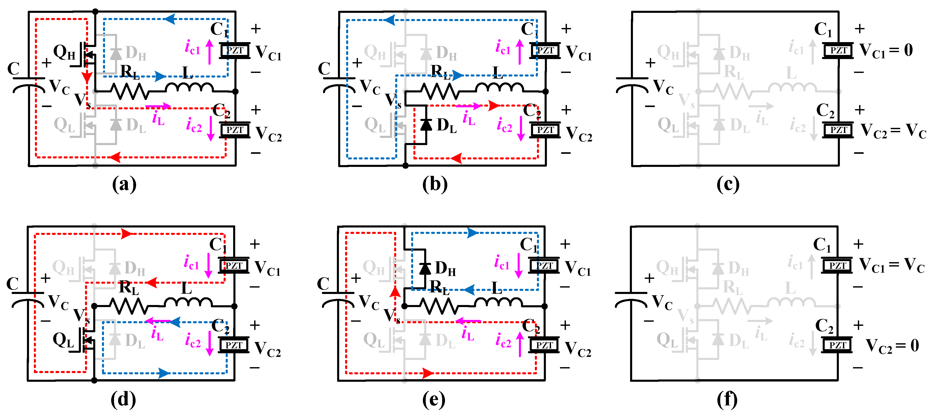
Unipolar signals of any shape can be generated by utilizing a half-bridge inverter that is composed of a high-quality factor inductor L and two inherent capacitors of the electrostatic actuators. Different operating modes of the high-voltage half-bridge drive stage are illustrated in Figure 6.
In mode (a), the inductor current iL begins to rise once the switch QH is turned on. The high-side equivalent capacitor C1 of the piezoelectric actuator starts to transfer the most unused energy to the low side, whereas the remaining energy is recovered in capacitor C. When the equivalent series resistance in a circuit is considered, the governing differential equations can be obtained as follows according to Kirchhoff’s voltage law:
When the two equations are combined, a second-order differential equation in this mode can be obtained as
where β = RL/2L is the neper frequency, and ω0 = 1/(2LC2)0.5 is the angular resonance frequency. Under an underdamped oscillation (β2 − ω02 < 0),
where the drive signal voltage vc2 is an underdamped voltage with a decaying oscillation at frequency ωd = (ω02 − β2)0.5. Mode (a) ends as soon as vc2 increases and becomes equal to VC in the first oscillation cycle.
At the end of mode (a), QH is turned off and the inductor current iL starts to decrease via the freewheeling diode DL. A new oscillation occurs between inductor L and the capacitive loads. The circuit starts operating alternatively in modes (b) and (e). The initial voltage in mode (b) is VC. The governing equations can be obtained as
Under an underdamped oscillation (β2 − ω02 < 0), the drive signal voltage becomes
where (vc2 (ta) = VC) represents the initial voltage condition at the end of mode (a) at ta. The drive signal voltage vc2 continues oscillating until it becomes stable and equal to VC during the rest of the period.
In mode (c), the lower side electrostatic actuator is completely charged, whereas the upper side electrostatic actuator is empty. The drive signal voltage vc2 is the same as VC during this period. All the unused energy is transferred from the upper side actuator to the lower side actuator, which enhances the overall efficiency of the system.
Mode (d) starts as soon as the transistor QL is turned on. The unused energy in the electrostatic actuator at the lower side begins to be transferred to the upper side. The inductor current iL rises reversely, thereby causing the discharge of the low side actuator C2. The underdamped drive signal vc2 descends with attenuated oscillation as follows:
Mode (d) ends as soon as vc2 drops to zero in the first oscillation cycle. At the end of mode (d), QL is turned off, and the inductor current iL increases through the freewheel diode DH. The circuit operates alternatively in modes (e) and (b). The initial voltage condition in mode (e) is zero. Similar to mode (b), the underdamped drive signal vc2 in mode (e) can be expressed as
where (vc2 (td) = 0) represents the initial voltage condition at the end of mode (d) at td. The high side actuator C1 is being charged by the stored energy of inductor L. After the oscillation ends, the drive signal vc2 becomes zero as soon as the inductor current turns zero until the next operation cycle begins.
In mode (f), the drive signal voltage vc1 is charged up to VC until the unused energy is fully transferred from the lower actuator to the upper one.
The inductor current iL, the drain-to-source voltage vds, and the drive voltage vc2 waveforms during each switching cycle are illustrated in Figure 7, with an operation sequence of a-b-e-b-c-d-e-b-e-f. Modes (a) and (d) are the modes at the beginning of two half-operation cycles. Modes (b) and (e) are the oscillation modes, which occur alternatively in both half-operation cycles. Modes (c) and (f) are the stable modes at the end of two half-operation cycles. Energy conversion is replaced by energy transfer in a working cycle. With the exception of the loss of the equivalent resistance of inductor iL, the half-bridge stage is a theoretically lossless structure that ensures high energy efficiency of the entire system.
3.3. Control Method of the Drive Stage
A traditional method used to generate a sinusoidal signal from a DC voltage is adopting an LC resonant network. For a sinusoidal PWM control technology, the inductor and two capacitors in a half-bridge inverter are generally required to have a large volume [30]. However, power density is particularly important for a miniaturized system in harsh applications, which is inconsistent with the ideal design for this study.
Janocha et al. considered the limitations of this method and proposed a control method for a reactive load (e.g., a piezoelectric actuator) to reduce the size of the inductor and meet the requirements for compactness [31]. In every switching cycle, the amplifier transfers the exact amount of energy that is necessary to achieve the desired output value at the load. This approach allows unnecessary switching cycles, thereby permitting higher system dynamics than those of converters using traditional (PWM or current mode) controllers.
However, this method is current-controlled. Therefore, the controller is required to calculate the switching time of the MOSFET. In such case, the parameters of the load and the components in the circuit should be determined in advance. If the parameters of the circuit are slightly changed, then the control method will become highly complicated.
A modified version of this method that can generate arbitrary waveform drive signals is embodied in this work through a four-phase control algorithm: Acquisition, Lookup, Charge, and Discharge.
During Acquisition, the output voltage is sampled using a resistive divider, which is regarded as the input of the analog comparator. In the Lookup phase, the sampled result and the desired value of Vo are used to generate a control pulse for switches QH and QL. The associated control architecture is shown in Figure 8.
When the output voltage is increased, the high-side power MOSFET is constantly turned on or off, which corresponds to the a–b cycle when energy is transferred to C2 in Figure 8. Conversely, it corresponds to the d–e cycle in Figure 6 when voltage drops. Apart from the amplitude of the drive signal, each working interval is timed by a timer overflow interruption when the frequency of the output signal requires adjustment.
4. Simulation Verification
To verify the feasibility of the circuit, its topology was simulated in the MATLAB Simulink environment. The specifications of the components used in the simulation are provided in Table 2. Among these, magnetizing inductance, output filter capacitor, resonant inductor, and transformer turn ratio are the same as those of the transformer and other circuit parameters used in subsequent experiments.
For the DC/DC stage, Figure 9 shows the simulated waveforms of the control signal of the power MOSFET Q, the input voltage Vbat, the currents Ip and Id through the primary and secondary sides of the transformer, and the output voltage Vc. Before the switch is turned on, the current through the rectifier diode drops to zero. Therefore, the circuit operates in DCM, which is consistent with the theoretical analysis.
The switching frequency of the MOSFET Q is 55.5 kHz. When Q is turned on, the primary inductance is linearly charged by the battery’s DC voltage of 3.7 V. During this phase, the current Id and the drain–source voltage vds of Q are both zero. When Q is turned off, the current Ip becomes zero, and the current of the rectifier diode Id starts to decrease from the maximum value Id/n. When the current Id drops to zero, the load is supplied by the output filter capacitor, and the primary and secondary sides of the transformer have zero current. When Q is turned on again, the new switching cycle of the operation is implemented.
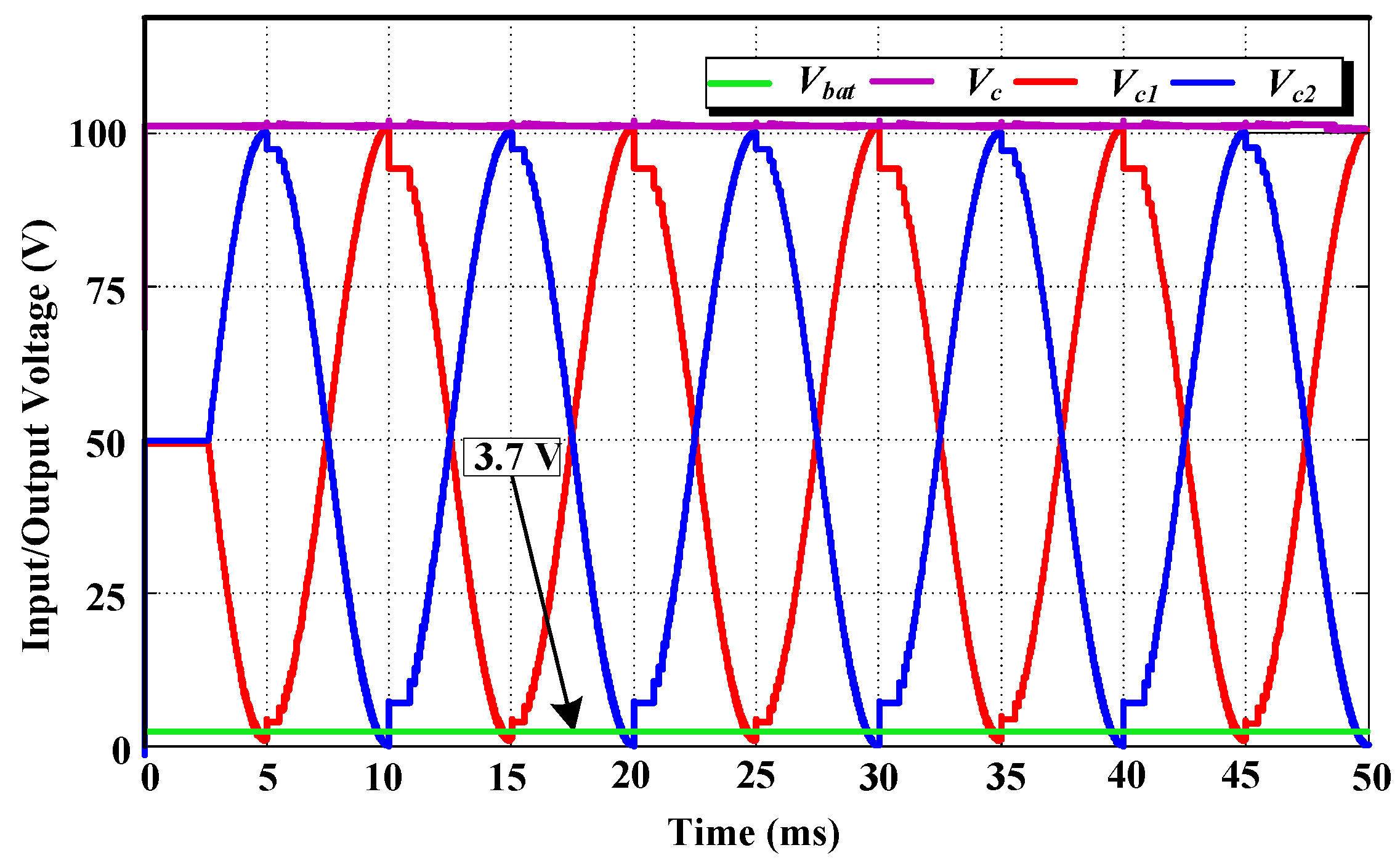
The voltage signals of Vc1 and Vc2 generated by the DC/AC half-bridge drive circuit should meet the requirements of drive signals for piezoelectric bimorph actuators. The simulation results in the DC/AC stage are presented in Figure 10. The voltages of Vc1 and Vc2 are 100 V sinusoidal signals with 100 Hz resonant frequency and 180° phase delay. In addition, various types of signals can be generated based on the design of the DC/AC circuit, including square, triangle, and sinusoidal signals.
5. Experiment Realization
5.1. Fabrication Specifications
The circuit topology described in Figure 4 is soldered onto a well-designed printed circuit board using discrete components. Table 3 lists the specifications of the discrete components, which include a power MOSFET, a rectifier diode, a flyback transformer, and a filtering capacitor. The flyback step-up stage is responsible for increasing the input DC voltage. The basis of the selection is to ensure that the components can handle the predicted voltage and current without breakdown and failure. As mentioned earlier, if the input voltage varies within the range of 3.0–4.5 V, then the maximum average current can reach 200 mA. Therefore, when the output is approximately 100 V, the average output current should be less than 10 mA. In accordance with package specifications, the N-channel enhancement MOSFET (SI2304, Vishay Intertechnology Inc., Shelton, CT, USA) with the small outline transistor (SOT) package is used as the primary side switch, because of its high voltage stress, low on-state resistance, and sufficient compactness.
The flyback secondary diode is an SOD-123 packaged Schottky barrier rectifier diode, i.e., SMD1200PL (Micro Commercial Components Inc., Simi Valley, CA, USA), which can withstand more than 1 A average forward current and up to 200 V reverse voltage. Compared with a conventional diode with a turn-on voltage of 0.7 V, SMD1200PL has a voltage of only 0.4 V at a forward current of 20 mA. Therefore, conduction loss is low, which is a key factor in selecting this diode.
The flyback transformer LPR4012 (Coilcraft Inc., Cary, IL, USA) with a weight of 64 mg and made of ferrite material produced by Coilcraft has an excellent coupling coefficient (>0.95) and good electromagnetic interference (EMI) performance. Its primary inductance is 2 μH and the turn ratio is 1:10, which can withstand a peak current of 1.7 A under an unsaturated condition. The 1 μF/200 V output filter capacitor (Vishay Intertechnology Inc., Shelton, CT, USA) with a 0603 package is selected to diminish voltage ripple on the actuator outputs.
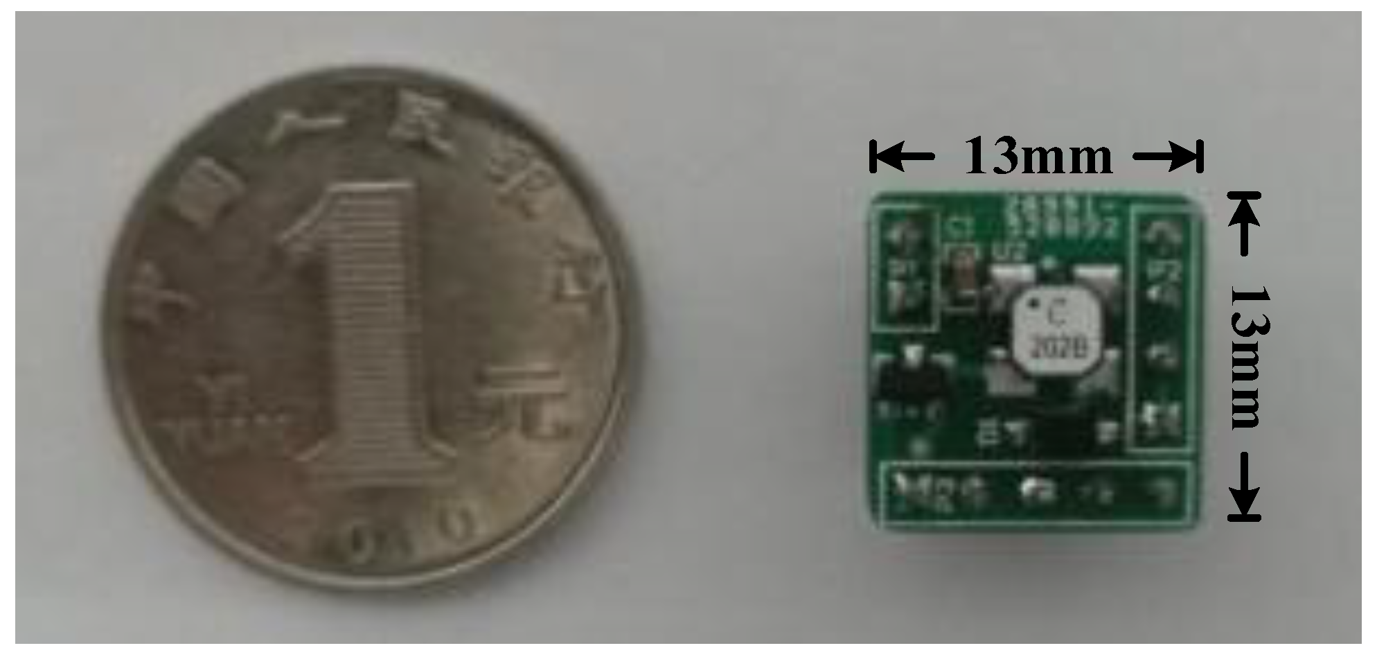
For the half-bridge drive circuit, two N-channel enhancement MOSFETs TN2404K (Vishay Intertechnology Inc., Shelton, CT, USA) with an SOT-23 package are adopted as high-side and low-side switches, because of their high capability to withstand voltage and low on-state resistance. A 0603 package passive inductor (Vishay Intertechnology Inc., Shelton, CT, USA) with a high quality factor and good EMI characteristic is used to obtain excellent output signals. The image of the fabricated converter is shown in Figure 11.
Using the above components, a prototype weighing 108 mg was fabricated. The length, width, and thickness of the circuit are 13, 13, and 4 mm, respectively. The converter realizes miniaturization at the gram level, thereby enabling it to meet the requirement of compactness for MMRs in harsh applications.
5.2. Circuit Experimental Analyses
A low-voltage source lithium battery is utilized to generate high drive voltage in the developed topology. The input voltage Vbat of the dual-stage drive circuit is 3.7 V, and the output voltage Vo is regulated at 100 V. One layer of the bimorph actuator can be modeled as a 48 nF capacitor in parallel with a few megaohm resistance. Multiple actuators are cascaded to increase load condition in circuit validation. The dual-stage converter is capable of driving capacitive loads at nanofarad level, with up to 0.5 W (full load) unipolar actuation.
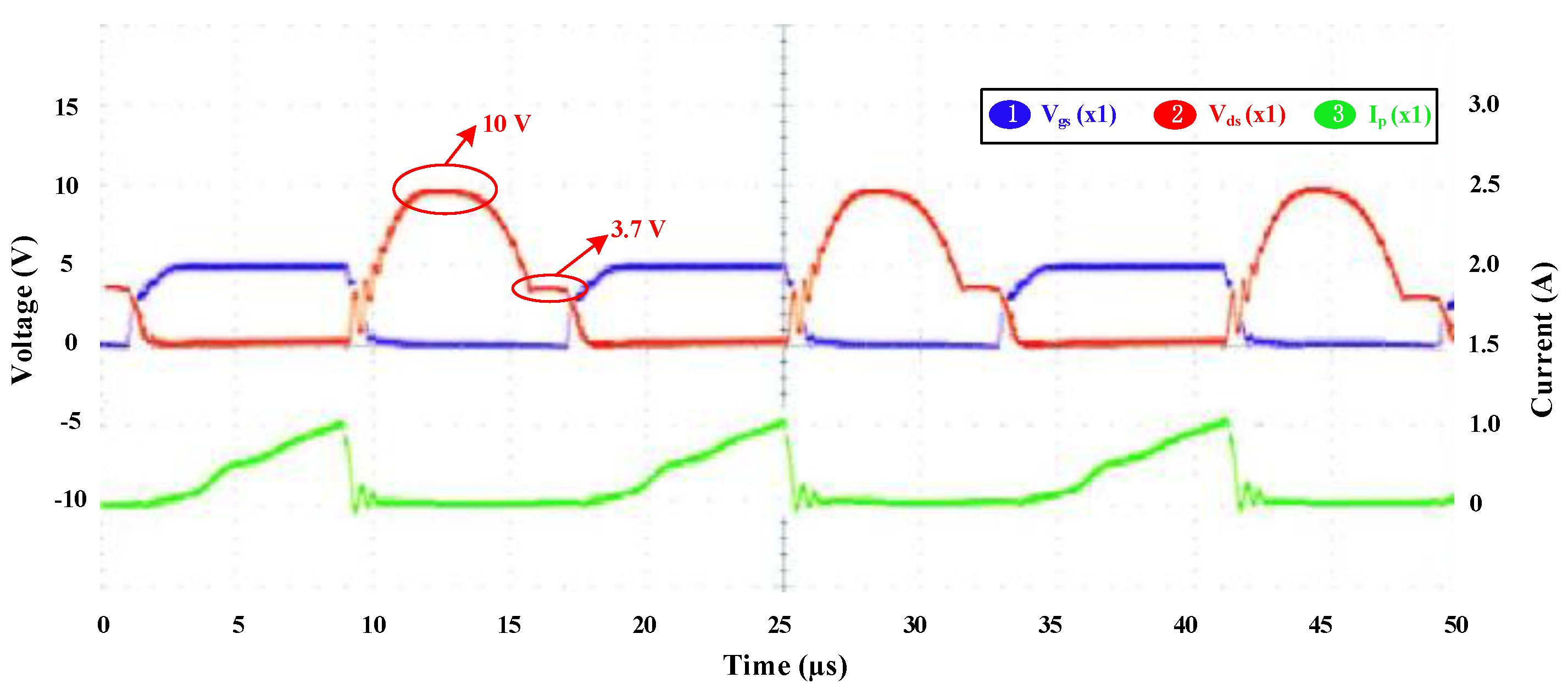
In the DC/DC stage, the node waveforms of Vgs (driven gate voltage), Vds, and Ip were obtained, as shown in Figure 12. The Ip current is fully provided by the lithium battery. The waveforms are consistent with the theoretical analysis. The maximum instantaneous output power of the lithium battery can reach four watts. The zero current shows that the flyback circuit worked in DCM mode.
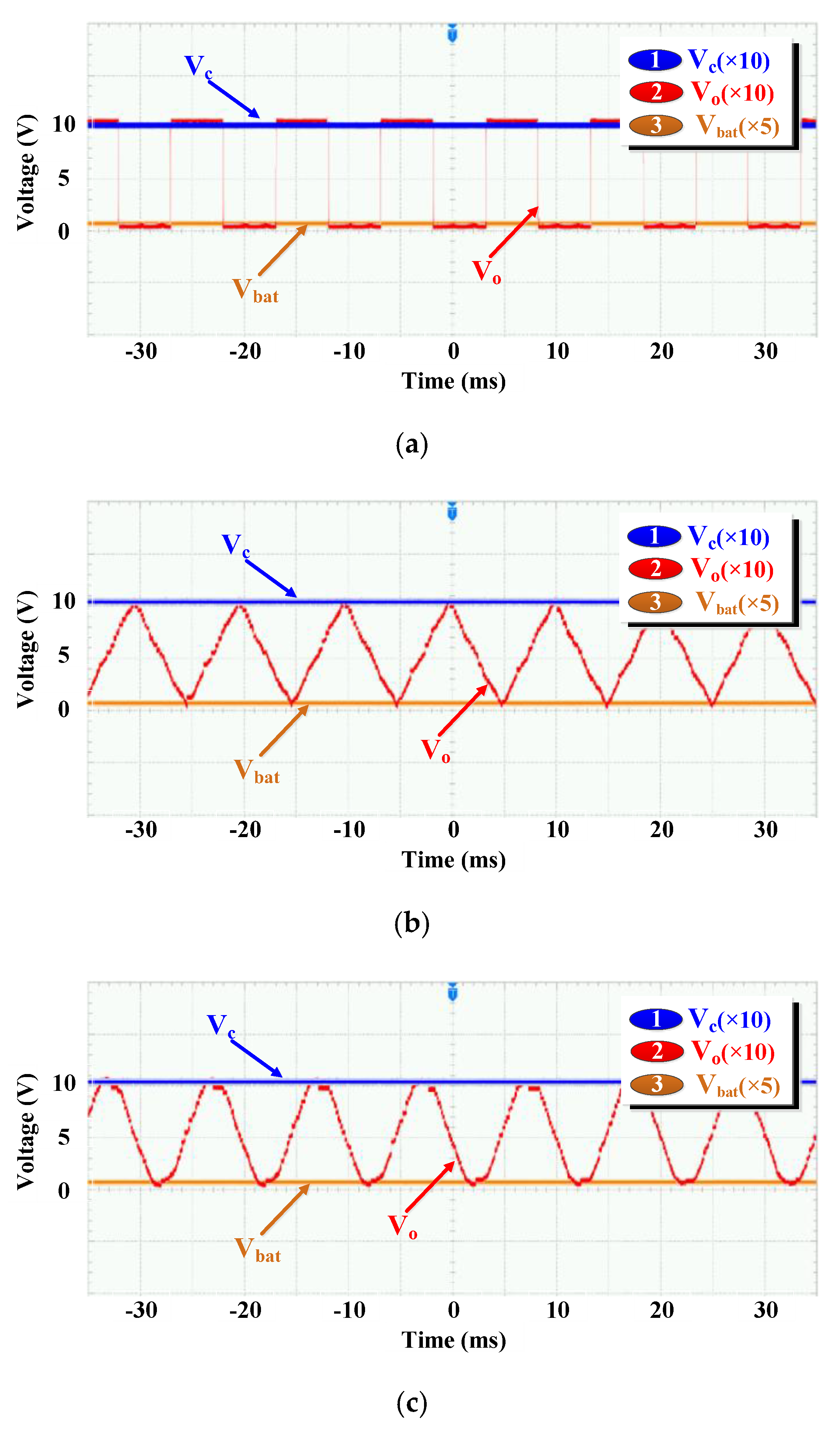
This circuit topology is capable of generating three waveforms (i.e., square, triangle, and sinusoidal waveforms; Figure 13). An oscilloscope probe is used five and ten times to measure a voltage of 100 V.
Figure 14 shows the output waveforms of the three signals and the corresponding control pulses of the two power MOSFETs. When the sinusoidal signal is used as an example, the timing pulses are turned on and the high-side transistor QH is constantly switched during the Charge phase, thereby initiating the transfer of energy to node Vo. During the Discharge phase, the low-side transistor QL is turned on and the high-side transistor QH is turned off, thereby lowering voltage Vo. As shown in the enlarged view, the switch is only turned on when the capacitor is required to reach the ideal voltage, thereby avoiding unnecessary switching actions and significantly reducing switching loss.
The proposed converter’s conversion efficiency can be calculated as follows:
where Pload is the average power of the PZT load, and Pin is the average input power of the developed converter.
Figure 15 demonstrates the efficiency of the proposed interface in terms of various loads and drive signal frequencies.
The loads continuously increase from 10% to 100% with 10% intervals. The three driving frequencies are 100, 110, and 120 Hz. The peak efficiency (64.5%) can be reached at 60% load and 100 Hz driving frequency (Figure 14), which is higher than the maximum conversion efficiency of 42.4% obtained in [9]. Table 4 outlines the electrical characteristics of the proposed drive circuit.
5.3. Performance Optimization
To optimize the parameters and improve circuit performance, energy efficiency optimization experiments of the DC/DC and DC/AC stages are conducted to understand the design tradeoffs. For the DC/DC step-up stage, four parameters, namely, magnetizing inductance, switching frequency, drive voltage, and output power, are considered as critical parameters that affect the efficiency of the circuit. Six flyback transformers with different magnetizing inductances are selected for the optimization test. In addition, switching frequency varies from 40 kHz to 200 kHz with 20 kHz steps. Within a drive voltage range of up to 160 V, the circuit changes from 20% load (0.1 W) to full load (0.5 W).
Figure 16 depicts the efficiency variation of the flyback stage with different magnetizing inductances and switching frequencies at 60% load and 90 V drive voltage. When the switching frequency is constant, a large magnetizing inductance results in high conversion efficiency, because a large magnetizing inductance can reduce current swing, thereby decreasing hysteresis eddy losses.
When magnetizing inductance is constant, switching frequency significantly affects conversion efficiency, as reflected in switching and iron losses. At low switching frequencies (<80 kHz), iron losses become dominant, due to the high magnetizing forces caused by a large current swing of the coupled inductors. A low switching frequency results in a small current swing, which reduces iron losses and improves system efficiency. However, MOSFET switching losses become dominant when operating at high switching frequencies (>80 kHz).
Figure 17 shows that at 60% load operation and 90 V drive voltage, a maximum efficiency of 81.8% is detected with 60 μH magnetizing inductance at 100 kHz switching frequency.
This figure illustrates how conversion efficiency varies with output power and drive voltage when switching frequency is 100 kHz and magnetizing inductance is 60 μH. Efficiency is measured under the condition that the output power range is 0.1–0.5 W and the drive voltage range is 40–160 V. At a low output power, parasitic MOSFET losses are dominant. When output power increases to a certain value, the conduction loss of a MOSFET and the copper loss of the transformer become dominant.
Under the condition of a constant load, low drive voltages lead to large currents, with conduction losses being dominant. At high drive voltages, conduction losses will be reduced in correspondence to the smaller currents, thereby increasing efficiency. When drive voltage exceeds a certain value, iron losses will become dominant, because of the large current swing caused by large duty cycles. Maximum efficiency occurs at nearly 0.3 W output power and 90 V driving voltage with a switching frequency of 100 kHz and a magnetizing inductance of 60 μH.
In the half-bridge stage, a high-quality factor inductor can effectively reduce conduction loss. Simultaneously, an inductance with a small value is selected to increase resonance frequency. Similar to the flyback converter, the experimental results exhibit high efficiency (ranging from 70.1% to 80.3%) under the desired operation as illustrated in Figure 18.
5.4. PZT Driving Validation
The dynamic performance of the fabricated converter was tested by observing the displacement of the piezoelectric bimorph (QDTE52-7.0-0.82-4, PANT, Suzhou, Jiangsu, China). Figure 19 shows the image of the entire system, which comprises a battery box, the proposed drive circuit, and a manual probe station that is used in conjunction with a B1505A I/V Agilent power device analyzer (Keysight Technologies, Inc., Santa Rosa, CA, USA). The output of the drive circuit is connected to the terminal of the probe, and the piezoelectric actuator is physically anchored by the terminal under the electron microscope.
The parameters of the piezoelectric bimorph used in the experiment are 52 × 7.0 × 0.82 mm (size), 1.2 mm (bidirectional displacement), 100 Hz (resonant frequency), and 200 V (maximum driving voltage). The displacement of the front end of the actuator at 0, 60, 80, and 100 V drive circuit was photographed using a high-speed camera and the images in (a)–(d) of Figure 20 present the corresponding observations. The figure shows that the displacement degree of the actuator increases as driving voltage increases. The arrow indicates the direction, in which 0.5 mm unidirectional displacement can be obtained when the actuator is applied at a drive voltage of 100 V.
Similarly, the bidirectional displacements, shown in Figure 21, are achieved with −100, 0, and 100 V excitation generated by the proposed circuit, which illustrate the piezoelectric bimorph at (a) down, (b) equilibrium, and (c) up, respectively. The experimental results show that the mechanical displacement is proportional to the square of the driving voltage. The displacement of the up–down motion is close to 1 mm, which can be further expanded by mechanically magnifying the structure to obtain potential applications in MMR.
6. Conclusion
In summary, this paper discusses a dual-stage converter that exhibits high performance at low mass and microsize for driving piezoelectric bimorphs at system level in MMR applications. The operations and control strategies of high step-up DC/DC stage and DC/AC driving stage are presented in detail. Combined with mechanical loads, the dual stage converter can fully utilize its many advantages to accomplish specific tasks, including, but not limited to, military reconnaissance and environmental monitoring. Future research will focus on reductions in circuit losses to improve efficiency and the miniaturization of prototypes. Simultaneously, a study on coupling theory of high-performance composites and piezoelectric ceramics will also be conducted to produce a piezoelectric composite actuator with lighter mass and higher strength energy density. With advanced drive technology, greater mechanical displacement is generated for MMR. For the drive circuit, custom bare die package components have potential uses when fabricated. On the basis of this study, the suppression of switching losses can be realized by using soft switching technology to improve the efficiency of a system.
Author Contributions
Y.W. conceived and designed the research. C.C. and M.L. performed the research. C.C. and M.L. wrote the paper.
Funding
This research was funded by the National Key R&D Program of China grant number: 2016YFC0303902, the Science and Technology Department of Jilin Province of China grant number: 20180201022GX, SXGJQY201711, and the Education Department of Jilin Province of China grant number: JJKH20180154KJ.
Acknowledgments
This research was supported by the National Key R&D Program of China (No. 2016YFC0303902), the Science and Technology Department of Jilin Province of China (Nos. 20180201022GX, SXGJQY201711), and the Education Department of Jilin Province of China (No. JJKH20180154KJ).
Conflicts of Interest
The authors declare no conflict of interest.
References
- Ceylan, H.; Giltinan, J.; Kozielski, K.; Sitti, M. Mobile microrobots for bioengineering applications. Lab Chip 2017, 17, 1705. [Google Scholar] [CrossRef] [PubMed]
- Gregory, J.; Fink, J.; Stump, E.; Twigg, J.; Rogers, J.; Baran, D.; Fung, N.; Young, S. Application of Multi-Robot Systems to Disaster-Relief Scenarios with Limited Communication. In Field and Service Robotics; David, W., Timothy, D.B., Eds.; Springer International Publishing: New York, NY, USA, 2016; pp. 639–653, 1610–7438. [Google Scholar]
- Cai, H.M.; Ang, H.S.; Zhang, H.L.; Duan, W.B. Experiment on aerodynamic characteristics of a novel micro tilt ducted fan aircraft with wings. Acta Autom. Sin. 2012, 30, 777–781. [Google Scholar]
- Rios, S.A.; Fleming, A.J.; Yong, Y.K. Design of a two degree of freedom resonant miniature robotic leg. In Proceedings of the IEEE International Conference on Advanced Intelligent Mechatronics, Busan, Korea, 7–11 July 2015; pp. 318–323. [Google Scholar]
- Tang, Y.; Chen, C.; Khaligh, A.; Penskiy, I.; Bergbreiter, S. An ultracompact dual-stage converter for driving electrostatic actuators in mobile microrobots. IEEE Trans. Power Electron. 2014, 29, 2991–3000. [Google Scholar] [CrossRef]
- Suzumori, K.; Endo, S.; Kanda, T.; Kato, N.; Suzuki, H. A Bending Pneumatic Rubber Actuator Realizing Soft-bodied Manta Swimming Robot. In Proceedings of the IEEE International Conference on Robotics and Automation, Roma, Italy, 21 May 2007; pp. 4975–4980. [Google Scholar]
- Lv, X.; Wei, W.; Mao, X.; Chen, Y.; Yang, J.; Yang, F. A novel MEMS electromagnetic actuator with large displacement. Sens. Actuators A 2015, 221, 22–28. [Google Scholar] [CrossRef] [Green Version]
- Mineta, T.; Mitsui, T.; Watanabe, Y.; Kobayashi, S.; Haga, Y.; Esashi, M. An active guide wire with shape memory alloy bending actuator fabricated by room temperature process. Sens. Actuators A 2002, 97–98, 632–637. [Google Scholar] [CrossRef]
- Towfighian, S.; Seleim, A.; Abdel-Rahman, E.M.; Heppler, G.R. A large-stroke electrostatic micro-actuator. J. Micromech. Microeng. 2011, 21, 075023. [Google Scholar] [CrossRef] [Green Version]
- Kovacs, G.; Düring, L.; Michel, S.; Terrasi, G. Stacked dielectric elastomer actuator for tensile force transmission. Sens. Actuators A 2009, 155, 299–307. [Google Scholar] [CrossRef]
- Wood, R.J.; Avadhanula, S.; Sahai, R.; Steltz, E.; Fearing, R.S. Micro robot Design Using Fiber Reinforced Composites. J. Mech. Des. 2008, 130, 680–682. [Google Scholar] [CrossRef]
- Karpelson, M.; Wei, G.Y.; Wood, R.J. Driving high voltage piezoelectric actuators in microrobotic applications. Sens. Actuators A 2012, 176, 78–89. [Google Scholar] [CrossRef]
- Nabawy, M.R.A.; Parslew, B.; Crowther, W.J. Dynamic performance of unimorph piezoelectric bending actuators. Proc. Inst. Mech. Eng. Part I J. Syst. Control Eng. 2015, 229, 118–129. [Google Scholar] [CrossRef]
- Nabawy, M.R.A.; Crowther, W.J. Dynamic electromechanical coupling of piezoelectric bending actuators. Micromachines 2016, 7, 12. [Google Scholar] [CrossRef]
- Steltz, E.; Seeman, M.; Avadhanula, S.; Fearing, R.S. Power electronics design choice for piezoelectric micro robots. In Proceedings of the IEEE/RSJ International Conference on Intelligent Robots and Systems, Beijing, China, 9–15 October 2006; pp. 1322–1328. [Google Scholar]
- Chen, C.; Liu, M.; Lin, J.; Wang, B.; Wang, Y. Piezoelectric transformer-based high conversion ratio interface for driving dielectric actuator in micro robotic applications. Int. J. Adv. Robot. Syst. 2016, 13. [Google Scholar] [CrossRef]
- Luo, F.L.; Ye, H. Positive output cascade boost converters. IEE Proc. Electr. Power Appl. 2004, 151, 590–606. [Google Scholar] [CrossRef]
- Liang, T.J.; Chen, S.M.; Yang, S.L.; Chen, J.F.; Ioinovici, A. A single switch boost-flyback dc-dc converter integrated with switched-capacitor cell. In Proceedings of the IEEE 8th International Conference on Power Electronics and Ecce Asia, Jeju, Korea, 30 May–3 June 2011; pp. 2782–2787. [Google Scholar]
- Liao, W.C.; Liang, T.J.; Liang, H.H.; Liao, H.K.; Juang, K.C.; Chen, J.F. Study and implementation of a novel bidirectional dc-dc converter with high conversion ratio. In Proceedings of the IEEE Energy Conversion Congress and Exposition, Phoenix, AZ, USA, 17–22 September 2011. [Google Scholar]
- Campolo, D.; Sitti, M.; Fearing, R.S. Efficient charge recovery method for driving piezoelectric actuators with quasi-square waves. IEEE Trans. Ultrason. Ferroelectr. Freq. Control 2003, 50, 237–244. [Google Scholar] [CrossRef] [PubMed] [Green Version]
- Edamana, B.; Oldham, K. Optimal on-off controller with charge recovery for thin-film piezoelectric actuators for an autonomous mobile micro-robot. In Proceedings of the American Controls Conference, San Francisco, CA, USA, 29 June–1 July 2011. [Google Scholar]
- Zsurzsan, G.T.; Zhang, Z.; Andersen, M.M.A.; Andersen, N.A. Class-D amplifier design and performance for driving a piezo actuator drive servomotor. In Proceedings of the IEEE International Conference on Industrial Technology (ICIT), Taipei, Taiwan, 14–17 March 2016. [Google Scholar]
- Clingman, J.C.; Gamble, M. High-voltage switching piezo drive amplifier. In Proceedings of the 5th Annual International Symposium on Smart Structures and Materials, San Diego, CA, USA, 1–5 March 1998. [Google Scholar]
- Luan, J. Design and Development of High-Frequency Switching Amplifiers Used for Smart Material Actuators with Current-Mode Control. Master’s Thesis, Virginia State University, Blacksburg, VA, USA, 29 July 1998. [Google Scholar]
- Gnad, G.; Kasper, R. Power Drive Circuits for Piezo-Electric Actuators in Automotive Applications. In Proceedings of the IEEE International Conference on Industrial Technology, Mumbai, India, 15–17 December 2006; pp. 1597–1600. [Google Scholar]
- Guan, M.; Liao, W.H. Studies on the circuit models of piezoelectric ceramics. In Proceedings of the International Conference on Information Acquisition, 2004, Proceedings, Hefei, China, 21–25 June 2004; pp. 26–31. [Google Scholar]
- Rios, S.A.; Fleming, A.J. A new electrical configuration for improving the range of piezoelectric bimorph benders. Sens. Actuators A 2015, 224, 106–110. [Google Scholar] [CrossRef]
- Small, high-voltage boost converters. Maxim Semiconductor Application Note 1109. 2002. Available online: https://www.maximintegrated.com/en/app-notes/index.mvp/id/1109 (accessed on 12 September 2018).
- Karpelson, M.; Whitney, J.P.; Wei, G.Y.; Wood, R.J. Design and Fabrication of Ultralight High-Voltage Power Circuits for Flapping-Wing Robotic Insects. In Proceedings of the Twenty-Sixth Annual IEEE Applied Power Electronics Conference and Exposition (APEC), Fort Worth, TX, USA, 6–11 March 2011; pp. 2070–2077. [Google Scholar]
- Honda, J.; Adams, J. Class D Audio Amplifier Basics. Amp Nch. 2005. International Rectifier Application Note AN-1071. Available online: https://www.infineon.com/dgdl/an-1071.pdf?fileId=5546d462533600a40153559538eb0ff1 (accessed on 12 September 2018).
- Janocha, H.; Stiebel, C. New approach to a switching amplifier for piezoelectric actuators. Energy 1998, 2, 2. [Google Scholar]
Figure 1.
Electrical equivalent model of piezoelectric element.

Figure 2.
Impedance characteristic of one layer of bimorph.

Figure 3.
Driving methods for piezoelectric actuators: (a) Bimorph with alternating driving; (b) bimorph with simultaneous driving.
Figure 3.
Driving methods for piezoelectric actuators: (a) Bimorph with alternating driving; (b) bimorph with simultaneous driving.

Figure 4.
Bidirectional converter topology and control architecture.

Figure 5.
Switching waveforms of the flyback converter during (a) one switching period; (b) steady-state operation.
Figure 5.
Switching waveforms of the flyback converter during (a) one switching period; (b) steady-state operation.

Figure 6.
Six switching modes of the high-voltage half-bridge drive stage.

Figure 7.
Switching pulse waveforms (QH and QL), drain-to-source voltage (vds), inductor current (iL), and output voltage (vc2) of the drive stage during one switching cycle.
Figure 7.
Switching pulse waveforms (QH and QL), drain-to-source voltage (vds), inductor current (iL), and output voltage (vc2) of the drive stage during one switching cycle.

Figure 8.
Inductor current, output voltage, and switching pulse waveforms during each half cycle.

Figure 9.
Simulation waveforms of each node in flyback DC/DC stage.

Figure 10.
Simulation waveforms of the drive stage.

Figure 11.
Image of the fabricated converter.

Figure 12.
Node waveforms of the flyback converter.

Figure 13.
Output voltages of each node (i.e., Vbat, Vc and Vo) in (a) square driving; (b) triangle driving; and (c) sinusoidal driving modes.
Figure 13.
Output voltages of each node (i.e., Vbat, Vc and Vo) in (a) square driving; (b) triangle driving; and (c) sinusoidal driving modes.

Figure 14.
Images of the control pulses and output waveforms.

Figure 15.
Efficiency vs. load for the three different driving frequencies.

Figure 16.
Conversion efficiency of flyback stage vs. switching frequency and magnetizing inductance.
Figure 16.
Conversion efficiency of flyback stage vs. switching frequency and magnetizing inductance.

Figure 17.
Conversion efficiency of the flyback stage vs. drive voltage and output power.

Figure 18.
Efficiency of the half-bridge stage vs. drive voltage and output power.

Figure 19.
Image of the entire system.

Figure 20.
Displacement images of the piezoelectric actuator driven at four different voltages: (a) 0 V; (b) 60 V; (c) 80 V; and (d) 100 V.
Figure 20.
Displacement images of the piezoelectric actuator driven at four different voltages: (a) 0 V; (b) 60 V; (c) 80 V; and (d) 100 V.

Figure 21.
Image of the piezoelectric actuator displacement: (a) Down; (b) at equilibrium; and (c) up.
Figure 21.
Image of the piezoelectric actuator displacement: (a) Down; (b) at equilibrium; and (c) up.


Table 1.
Equivalent parameters of the bimorph actuator.
| Static Parameters | Value | Dynamic Parameters | Mode 1 | Mode 2 | Mode 3 | Mode 4 |
|---|---|---|---|---|---|---|
| C0 | 24 nF | Ln | 580 H | 812 mH | 422 mH | 15 mH |
| Rs | 1Ω | Cn | 3 nF | 2.85 nF | 1.9 nF | 3 nF |
| Rp | 10 MΩ | Rn | 8.5 MΩ | 7.5 MΩ | 6.7 MΩ | 5.2 MΩ |
Table 2.
Specifications of the utilized components.
| Components | Specifications |
|---|---|
| Vbat | 3.7 V |
| fs (switching frequency) | 55.5 kHz |
| D (duty cycle) | 50% |
| n (turn ratio) | 1:10 |
| Lm | 2 μH |
| C | 1 μF |
| L | 15 μH |
| C1,C2 | 48 nF |
Table 3.
Specifications of the discrete components.
| Device Name | Chip Number | Weight (mg) | Size (mm) |
|---|---|---|---|
| Flyback transformer | lpr4012 (Lm = 2 μH) | 64 | 4 × 4 |
| Power MOSFET (power stage) | SI2304 | 8 | 2.8 × 2.1 |
| Rectifier diode | SMD1200PL | 8 | 2.8 × 2.1 |
| Capacitor (power stage) | 1 μF/200 V | 1.2 | 1.6 × 0.8 |
| Power MOSFET (drive stage) | TN2404K | 8 | 2.8 × 2.1 |
| Inductor (drive stage) | 15 μH/40 mA | 1.2 | 1.6 × 0.8 |
Table 4.
Specific characteristics of the dual-stage circuit.
| Output Power (maximum) | 500 mW |
| Efficiency (maximum) | 64.5% |
© 2018 by the authors. Licensee MDPI, Basel, Switzerland. This article is an open access article distributed under the terms and conditions of the Creative Commons Attribution (CC BY) license (http://creativecommons.org/licenses/by/4.0/).
Share and Cite
MDPI and ACS Style
Chen, C.; Liu, M.; Wang, Y. A Dual Stage Low Power Converter Driving for Piezoelectric Actuator Applied in Micro Mobile Robot. Appl. Sci. 2018, 8, 1666. https://0-doi-org.brum.beds.ac.uk/10.3390/app8091666
AMA Style
Chen C, Liu M, Wang Y. A Dual Stage Low Power Converter Driving for Piezoelectric Actuator Applied in Micro Mobile Robot. Applied Sciences. 2018; 8(9):1666. https://0-doi-org.brum.beds.ac.uk/10.3390/app8091666
Chicago/Turabian StyleChen, Chen, Meng Liu, and Yanzhang Wang. 2018. "A Dual Stage Low Power Converter Driving for Piezoelectric Actuator Applied in Micro Mobile Robot" Applied Sciences 8, no. 9: 1666. https://0-doi-org.brum.beds.ac.uk/10.3390/app8091666
Note that from the first issue of 2016, this journal uses article numbers instead of page numbers. See further details here.