Ablation and Patterning of Carbon Nanotube Film by Femtosecond Laser Irradiation


1
School of Mechanical and Power Engineering, Harbin University of Science and Technology, Harbin 150080, China
2
School of Mechatronics Engineering, Harbin Institute of Technology, Harbin 150001, China
*
Author to whom correspondence should be addressed.
Appl. Sci. 2019, 9(15), 3045; https://0-doi-org.brum.beds.ac.uk/10.3390/app9153045
Submission received: 24 June 2019
/
Revised: 23 July 2019
/
Accepted: 25 July 2019
/
Published: 28 July 2019
(This article belongs to the Special Issue Laser Processing and Advanced Manufacturing of Microscale Energy Storage Devices)
Abstract
:Carbon nanotube (CNT) film can be used as thin film electrodes and wearable electronic devices due to their excellent mechanical and electrical properties. The femtosecond laser has the characteristics of an ultra-short pulse duration and an ultra-high peak power, and it is one of the most suitable methods for film material processing. The ablation and patterning of CNT film are performed by a femtosecond laser with different parameters. An ablation threshold of 25 mJ/cm2 was obtained by investigating the effects of laser pulse energy and pulse number on ablation holes. Raman spectroscopy and scanning electron microscope (SEM) were used to characterize the performance of the pattern groove. The results show that the oligomer in the CNT film was removed by the laser ablation, resulting in an increase in Raman G band intensity. As the laser increased, the ablation of the CNTs was caused by the energy of photons interacting with laser-induced thermal elasticity when the pulse energy was increased enough to destroy the carbon–carbon bonds between different carbon atoms. Impurities and amorphous carbon were found at and near the cut edge while laser cutting at high energy, and considerable distortion and tensile was produced on the edge of the CNTs’ groove. Furthermore, appropriate cutting parameters were obtained without introducing defects and damage to the substrate, which provides a practical method applied to large-area patterning machining of CNT film.
1. Introduction
The development of thin-film optoelectronic devices mainly depends on the achievements of materials science in the development of nanomaterials. These materials should have low electrical resistance characteristics combined with excellent flexibility, low weight, and, preferably, being manufactured by a simple and cost-effective method. Carbon nanotube (CNT) film is made of a coaxial tubular carbon molecular structure—carbon nanotubes [1] are one of those meet these requirements. They have been extensively exploited for a wide range of applications such as electron field emitters and flexible electronic devices. For example, they is used as a flexible device material and an energy-absorbing layer [2]. Due to the high elasticity and compressibility of CNT film, its original length is restored after their load is released, and their compression and recovery are repeated without cracking. Transparent single-walled carbon nanotube (SWCNT) film has high conductivity, and excellent flexibility can be regarded as an ideal alternative material which to indium tin oxide in electroluminescent devices and flexible electronic components [3]. CNT film can be used to make a supercapacitor because of their excellent flexibility, lightweight and corrosion resistance [4]. With the absorption characteristics of photons and the high power conversion efficiency of CNT film, significant progress has been made in solar cells [5] and thin-film transistors [6] applied to photosensitive LED (Light Emitting Diode) circuits. CNT film can also be used for thermal management materials applied in wearable electronics [7].
Flexible printed CNT film can be used as a transistor because of its physical stability, high carrier mobility and excellent mechanical flexibility. However, it is still a challenge to achieve high-performance with printed SWCNT film transistors with excellent mechanical flexibility [6]. How to efficiently and accurately make CNT film materials into specified sizes and structures is one of the constraints of the application and development of CNT film. At present, cutting methods include liquid-phase oxidation cutting, mechanical cutting, electron-beam-induced cutting and laser cutting [8], but these cutting methods have certain drawbacks. The liquid-phase oxidation cutting method will produce a large amount of material loss to CNT film. The surface of the material is concave at the cutting point due to mechanical stress in the mechanical cutting, resulting in uneven surface quality. Electron-beam-induced cutting can achieve a high cutting precision, but severe cutting conditions, complicated equipment, and high cost restrict the mass production of CNT film.
Compared with these process, laser direct cutting has several advantages, such as non-contact, maskless, and high precision processes. There have been several investigations about the laser cutting of CNT film. A laser can be used to pattern source/drain electrodes after fabricating source-drain electrodes using printable CNT ink which can reduce the overall cost of printed electronic devices. Gbordzoe S. et al. [8] reported that nanosecond laser cut CNT film can achieve a micron-scale processing size, but amorphous carbon is produced around the edge and ablated line, which affects the mechanical properties of CNT film. Bobrinetskiy I.I. et al. [9] used a picosecond pulsed laser with an energy close to the ablation threshold to ablate CNT film. Their results showed that an ultrafast pulsed laser induces the two-photon nonlinear oxidation of carbon–carbon bonds. P-type doping on the surface of the material makes the intensity of G band increase and shift to slightly lower wavenumbers in Raman spectroscopy. A multi-beam interference nanosecond laser can be used to ablate CNT film deposited on a glass substrate, as the width of the ablation region increases as the laser energy increases and the position at the maximum laser interference causes defects [10].
A femtosecond laser, which has the advantage of precise ablation with little or no thermal impact on surrounding materials [11,12], can overcome the above shortcomings as an ultra-short-pulse laser. A femtosecond laser has been widely used in many fields, such as the processing of various materials [13,14] and the fabrication of micro-components [15,16,17], because of its unique processing characteristics. Yoon, J.W. et al. [18] used a femtosecond laser to process a thin film of silver nanowires and CNTs. The edge of the cutting position is not uniform due to the different thresholds of Ag and CNTs, but it can be reduced by laser beam shaping in the edge deformation zone of the composite film. Cumulative effects induced by increasing number of laser pulses and ripples originate from the interference between the incident laser light and the scattered tangential wave are observed in the ablation of CNT film [19]. The material at the edge of the cutting position are damaged by femtosecond laser processing. Kalita, G. et al. [20] used Raman spectroscopy to detect the cutting position under the femtosecond laser direct patterning of graphene film. D band intensity increased significantly, since there was a relaxation of the backscattering condition with an induced defect at the edge of the graphene sheet. However, there has been relatively little research on the influence of laser parameters on cutting quality and defects in the femtosecond laser machining of CNT film.
This work aimed to explore the mechanism and influencing factors in the ablation and cutting process for the femtosecond laser machining of CNT film. Experiments were conducted to obtain the threshold of CNT film and the influence of cutting parameters on machining results. Specific features of the SEM and Raman spectrum were discussed to analyze the ablation mechanism and machining quality. Furthermore, preferred processing parameters were selected to cut the microstructure of CNT film with good cutting quality. This paves the way to advance the possible applications of CNT film in the field of the flexible electronic devices and conductive film.
2. Experiments
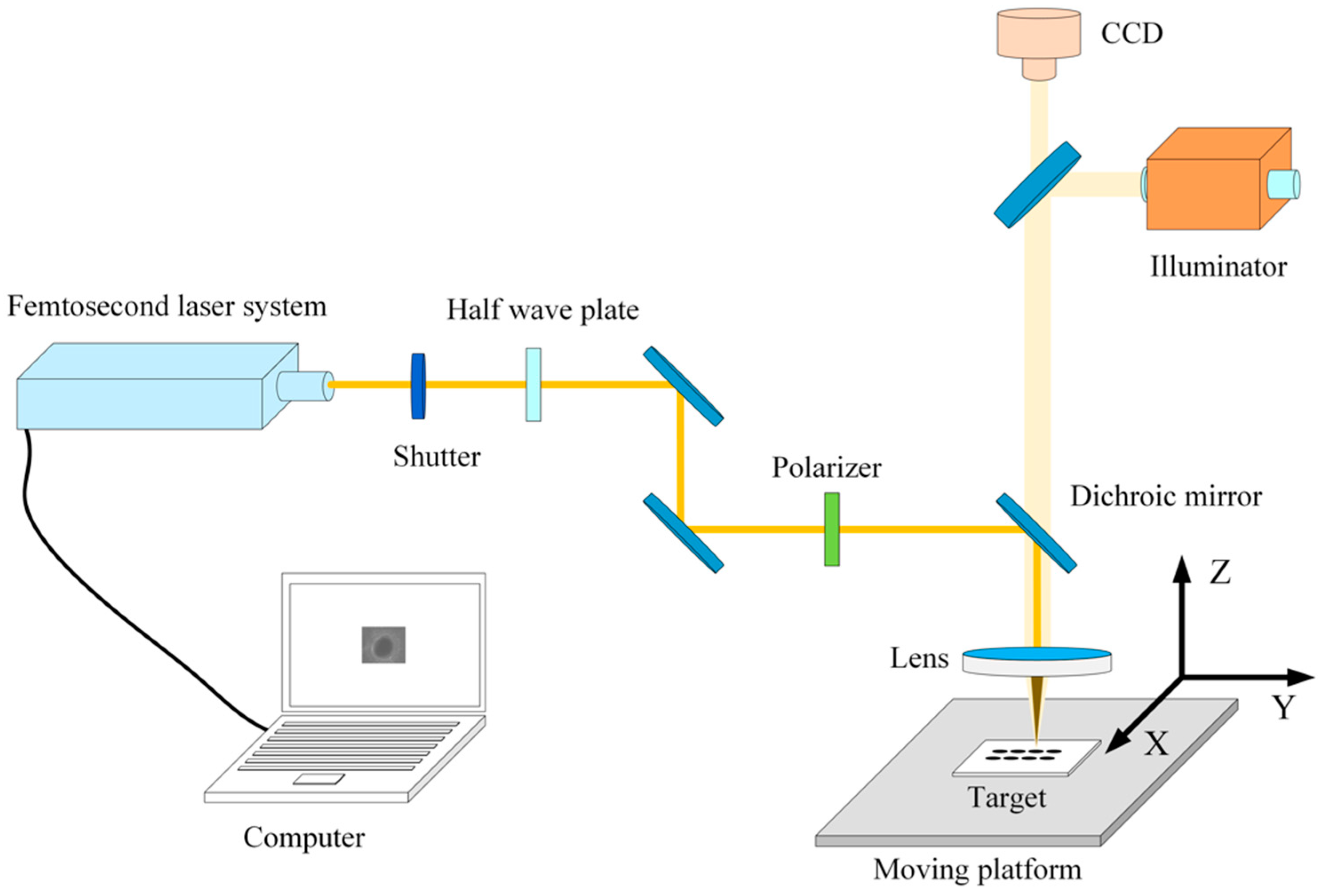
The sample used in the experiment was CNT film, which was produced by the floating catalytic chemical vapor deposition method [21], provided by the Suzhou Institute of Nano-Tech and Nano-Bionics, China. The thickness of the film was 10 μm, the sheet resistance was 2 × 10⁻⁵ Ω·cm, and the thermal conductivity of the CNT film was 700 W·m−1·K−1, which could be detected by frequency-domain thermoreflectance [22]. The oxygen-containing alkanes and olefin oligomers were contained to bond the CNTs and the transmittance less than 5% at the laser λ = 1030 nm [23]. The sample used a small amount of water vapor to atomize the surface of the spring steel substrate and to flatten the 10 μm thick CNT film on the spring steel substrate with a size of 2 × 2 cm. After standing for about 2 h, the sample was placed on an X–Y translation stage with a movement resolving power of 1 μm.
A femtosecond laser system, which has automated harmonics generators module mounts directly on the pharos PH1-15 laser head and integrated into the system, was used in the experiments. The process parameters are the wavelength of 1030 nm and 515 nm, pulse duration of 300 fs, and the repetition rate range from 1 kHz to 1 MHz. The maximum of pulse energy was 400 μJ. The energy profile of the laser beam was a Gaussian function profile, and the polarization state was linearly polarized. A schematic diagram of the experimental setup with femtosecond laser ablating is illustrated in Figure 1. The laser beam was directly focused on the surface of the CNT film by using optical lenses with a focal length of 60 mm, and the focal spot diameter was about 11 μm. The pulses number irradiated on the targets were precisely controlled by an electrical mechanical shutter synchronized with the laser repetition rate. A high-resolution visualization of the laser ablated region on the target surface was allowed by an accurate imaging system with a CCD camera (DelphiLaser). The laser output power was examined with a power meter before each test. Every ablating and cutting process were repeated 3 times, and each measurement was conducted at least 5 times on different areas. After laser ablating, the characteristics of the CNT film were examined by SEM (ZEISS Merlin Compact) and Raman spectrometer (Renishaw inVia). Raman spectra were collected on the cutting position of the raw film, the excitation laser power is 0.5 mW (532 nm wavelength), and the diameter of the exciting laser beam on the film surface was about 1 μm.
3. Results and Discussions
3.1. Ablation Threshold of CNT Film
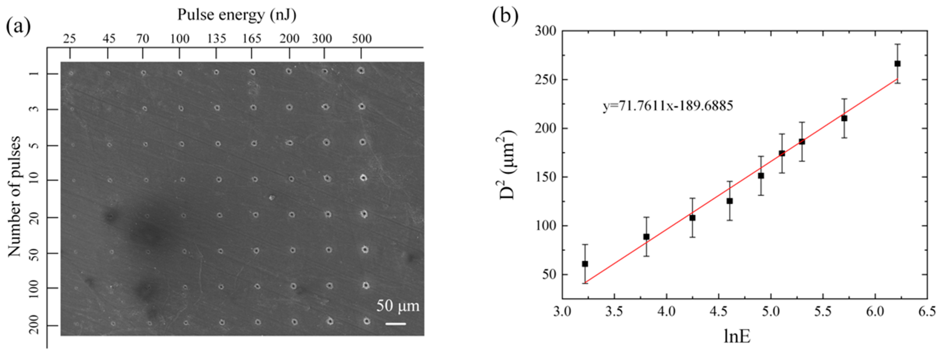
The ablation of the laser caused damage to the CNTs due to the interaction between the femtosecond laser and the CNT film. The ablation threshold is the minimum energy required to remove a single layer of material with irreversibly destroyed, and it is an essential parameter for CNT film. CNT film is composed of a large number of CNTs with different diameters and lengths. With an increase of laser pulse energy, different sizes of micro holes are produced on the surface of CNT film. The diameter can be directly measured, so a D2 method based on the energy conservation for measuring the threshold of material was used.
According to the Gaussian beam profile and the theoretical threshold behavior of the material, the relationship between the diameter of the modified area and the laser pulse energy can be expressed as [24]:
where D represents the diameter of the modified area (μm), ω0 is the waist radius of laser beam (μm), ϕth is the threshold fluence of the material (J/cm2), and ϕ0 is the energy density of the beam at the focal plane (J/cm2).
After applying the value of laser pulse energy E into the equation,
After rearranging the equation by plotting D2 versus lnE on the scale, a linear relationship can be obtained,
By fitting Equation (3) to the experimental data, the beam waist radius ω0 can be obtained by the slope of the fitting line, and ϕth is given by the interception of the regression curve. The x-coordinate and the laser energy density can be converted through .
After experiments, the diameter of the holes can be measured by SEM. The SEM image of the ablated areas on the CNT film for different pulse energies and the fitting relationship between the logarithm of the incident laser energy and the square of the ablation diameter are shown in Figure 2. A beam waist radius of 5.99 μm and ablation threshold of 25 mJ/cm2 were obtained by linear regression.
3.2. Analysis of Material Ablation Characteristics by Femtosecond Laser
3.2.1. Ablation Morphology of CNT Film Irradiated by Different Laser Pulse Energy and Number
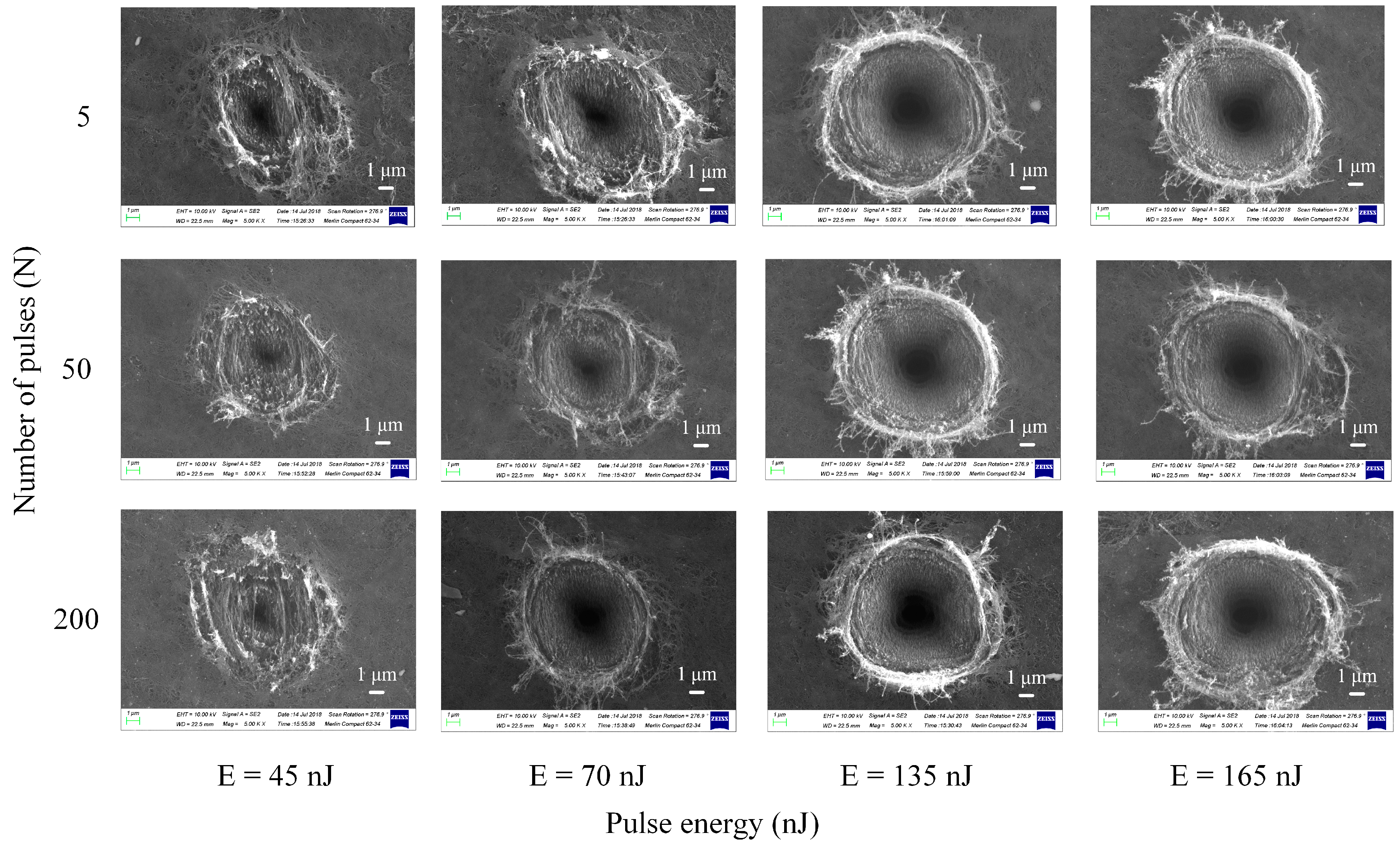
There are many factors influencing the interaction process between the femtosecond laser and material [13], such as the laser pulse energy and the number of pulses. The energy in the center of the spot is the highest, and the laser energy decreases away from the center of the spot due to the Gaussian distribution of laser intensity. Therefore, a morphology similar to a crater could be seen in the SEM image, as shown in Figure 3. Ablated CNT films with different pulse numbers (N = 5, 50, 200) were obtained under the pulse energy (E) of 45, 70, 135, and 165 nJ, respectively.
When the pulse energy was 45 nJ, the tightness of the CNTs at the edge of the ablation hole was reduced, and some oligomers used for bonding were removed. The diameter of the hole was small, and the shape was irregular at low pulse energy. By increasing the number of pulses, the ablation region gradually formed as the crater but did not change. Obviously, when the pulse energy increased to 70 nJ, the ablation area of the micro holes gradually increased with the increase of the laser energy, and the oligomer ablation area at the edge of the ablation hole gradually disappeared. Especially at the pulse energies of 135 and 165 nJ, a large amount of CNT filaments were present around the ablation holes, and distinct bright spots at the boundary of ablation holes could be observed by SEM.
The above phenomenon was mainly caused by the Gaussian distribution of the incident laser energy, and the cumulative effect of femtosecond laser on the CNT film was weak. When the number of pulses was five and the pulse energy was 45 nJ, the energy of the incident laser pulse was close to the ablation threshold of the material, the hydrocarbon oligomer in the CNT film was preferentially removed. The spot area where the incident region of the beam reached the ablation threshold of CNTs was small, resulting in a poor quality of the ablation hole.
As the pulse energy gradually increased to 165 nJ, ablation holes became regular and the depth increased. Meanwhile, the pulse energy density at the edge of the spot reached the ablation threshold of the CNT film, and the diameter of the hole began to increase. Moreover, the laser reached an in-deep layer after the surface was removed, so that the vaporization of the in-depth material was reversely sprayed off the body under the actions of high temperature and high pressure. The vaporized materials re-solidified on the edge of the ablation hole to form a bright spot structure with the partially fractured CNTs thrown around the hole under the force generated by a thermo elastic shock wave. Different pulse energies and different numbers of pulses were used in the experiments to analyze the influence of pulse number on the diameter of the ablation holes.
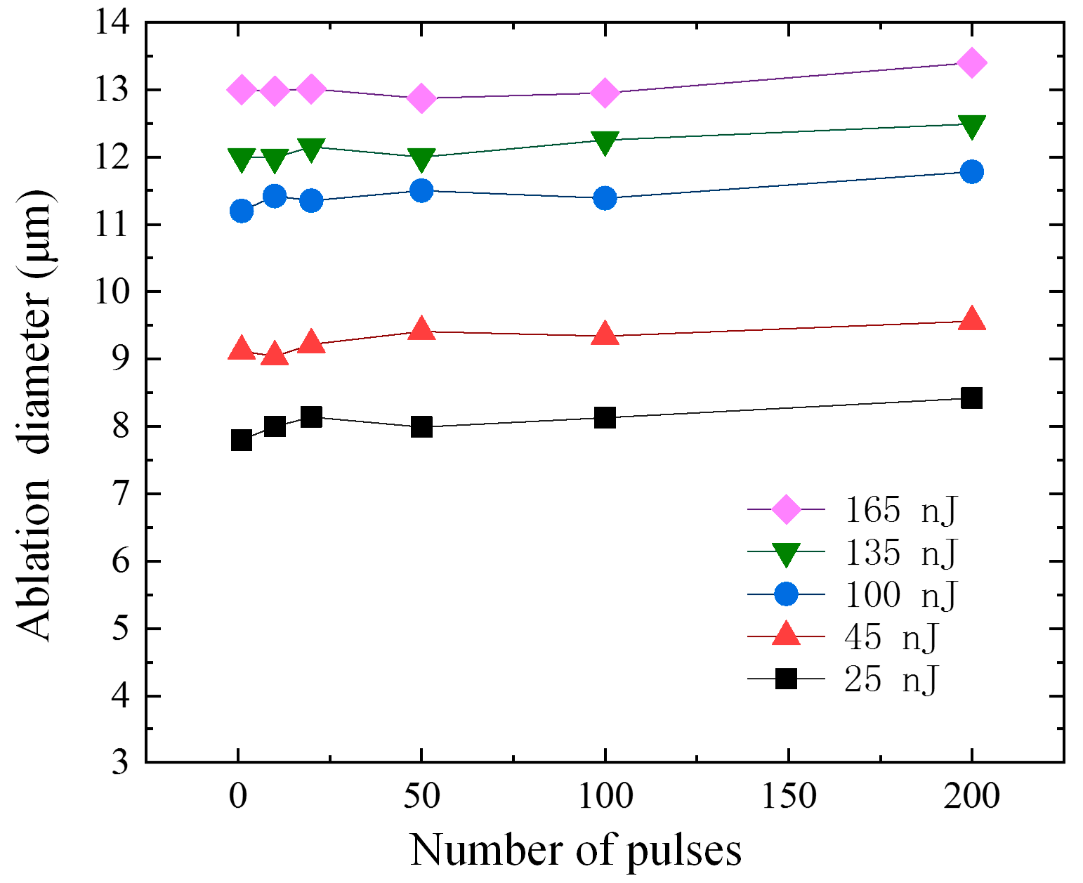
The diameter of the ablation hole changed with the increasing number of pules at different pulse energies, as shown in Figure 4. When the pulse energy was 25 nJ, the minimum diameter of the hole was 7.8 μm, and it increased with the increasing of the number of pulses. However, the ablation diameter increase was not significant. When the pulse energy was 165 nJ, the diameter of the hole was 12.9 μm, and the energy was far exceeded the ablation threshold of the material. Thus, increasing the number of pulses did not have a substantial effect on the diameter of the ablation hole. This result was related to the interaction between the laser and the material—the area of the region where the material ablation threshold reached was relatively stable. When the energy was low, the laser energy irradiated at the edge of the spot could not reach the ablation threshold of the material, and the partial material at the center of the spot was removed by ablation.
As the number of pulses increased, the energy at the center of the spot was absorbed by the inner wall of the material micro holes, which disturbed the interaction between the laser and the underlying material, resulting in the affection to the removal of materials and reducing the quality of processing. When the energy far exceeded the ablation threshold of the material, the area reaching the material ablation threshold increased, leading to an increase of the ablation area. However, the laser energy transferred to the deep layer of the CNT film as the number of pulses increased, and the lower energy of the edge region of the spot did not cause an ablation of the material, so the variation of the diameter was small.
3.2.2. Mechanisms of Femtosecond Laser Ablation of CNT Film
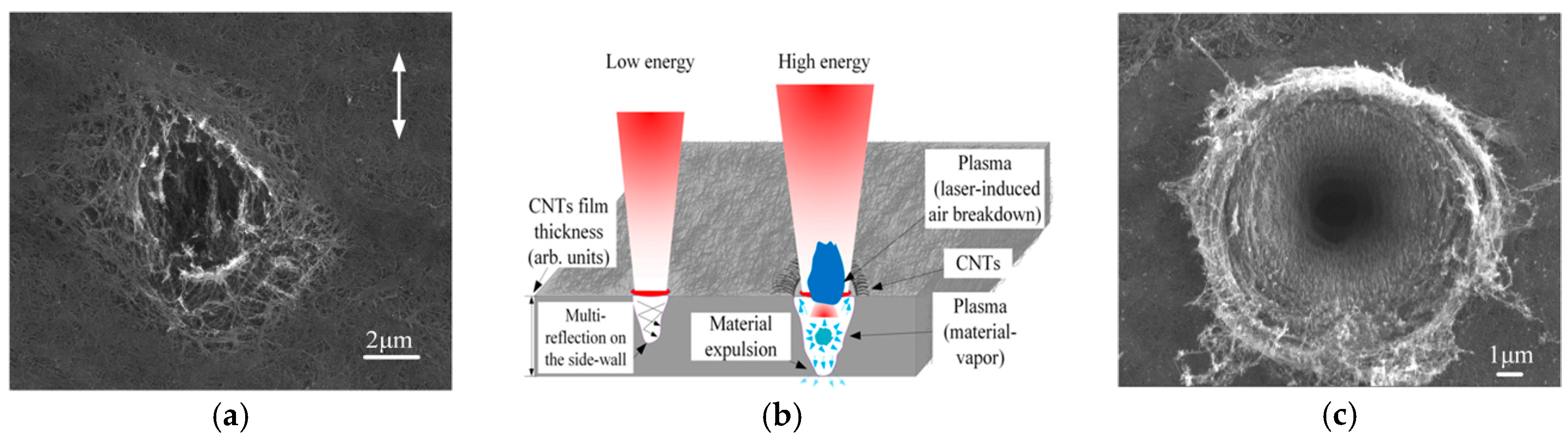
The large thermal stress caused by the laser irradiated on the CNT film will induce damage to the material, which may lead to complex structural modifications or even a conversion to other polymers [25]. Based on the analysis of the effect of laser parameters on the material, the surface morphology of the hole and the shape of the inner wall were mainly caused by the involved interaction mechanisms between the ultra-short pulse laser and the material. Figure 5 shows the morphology (the number of pulses was 200) and ablation schematics of CNT film by different laser energies.
When the laser pulse energy was low, the vaporization of the oligomer on the surface of the CNT film occurred during the pulse ablating process. The CNTs and the oligomer at the center of the spot were simultaneously removed due to the Gaussian distribution of laser intensity. However, the lower energy on the outer edge of the spot only could cause the oligomer to be removed, and the surface material on the spot became loose and porous, which was favorable for the escape of the vapor. Carbon–carbon bonds between different carbon atoms in CNTs broke by absorbing photon energy. The pulse energies changed their interatomic distance and broke their bonds with the surrounding atoms [26]. The CNTs jet produced by laser ablation and unbroken CNTs formed complex hole structures that affected the energy density acting on the material and could not exceed the damage threshold of the material, thus resulting in the small influence of the number of pulses on ablation depth. When the laser pulse energy was high, the increasing number of pulses made more energy deposited on the inner wall, thus accelerating the ablation of the material and eventually forming a through hole. At the same total fluence of a laser, multi-pulse ablation can reduce the compressive stress and tensile stress at the ablation position of film [27]. A laser can easily cause air to breakdown near the processed micro holes to form atmospheric plasma, and the laser intensity gradually decreases with the direction of the beam propagation. The laser energy irradiated on the inner wall of the processed hole cannot remove all the material, so the diameter of the bottom will be smaller than the entrance of the ablated hole [28].
During the laser ablation of the CNT film, laser-induced air breakdown and material vaporization in the holes created an enormous pressure, which will caused the ejection of the vaporized material from the ablated hole. The ejection material was rapidly condensed on the edge of hole under the effect of cooling air. Since the CNT film was composed of a large number of CNTs and oligomers, the fractured CNTs caused by laser ablation were thrown outside the hole under the pressure to form a projection of the outer edge of the CNT ablation hole.
At the same time, after forming a through hole, the plasma formed by the laser-induced air breakdown suppressed the corrosion flowing back to the inlet of the ablation hole. As such, most of the vapor escaped from the bottom of the ablation hole. This was related to the carbon–carbon bond in the low-energy destruction CNT layer described in the literature [29]. At a higher laser pulse energy and number of pulses, the nanotubes were transformed into different nanocarbon forms, e.g., carbon nanoparticles and small carbon clusters [30].
3.3. Femtosecond Laser Cutting CNT Film
3.3.1. Raman Analysis of Femtosecond Laser Cutting CNT Film
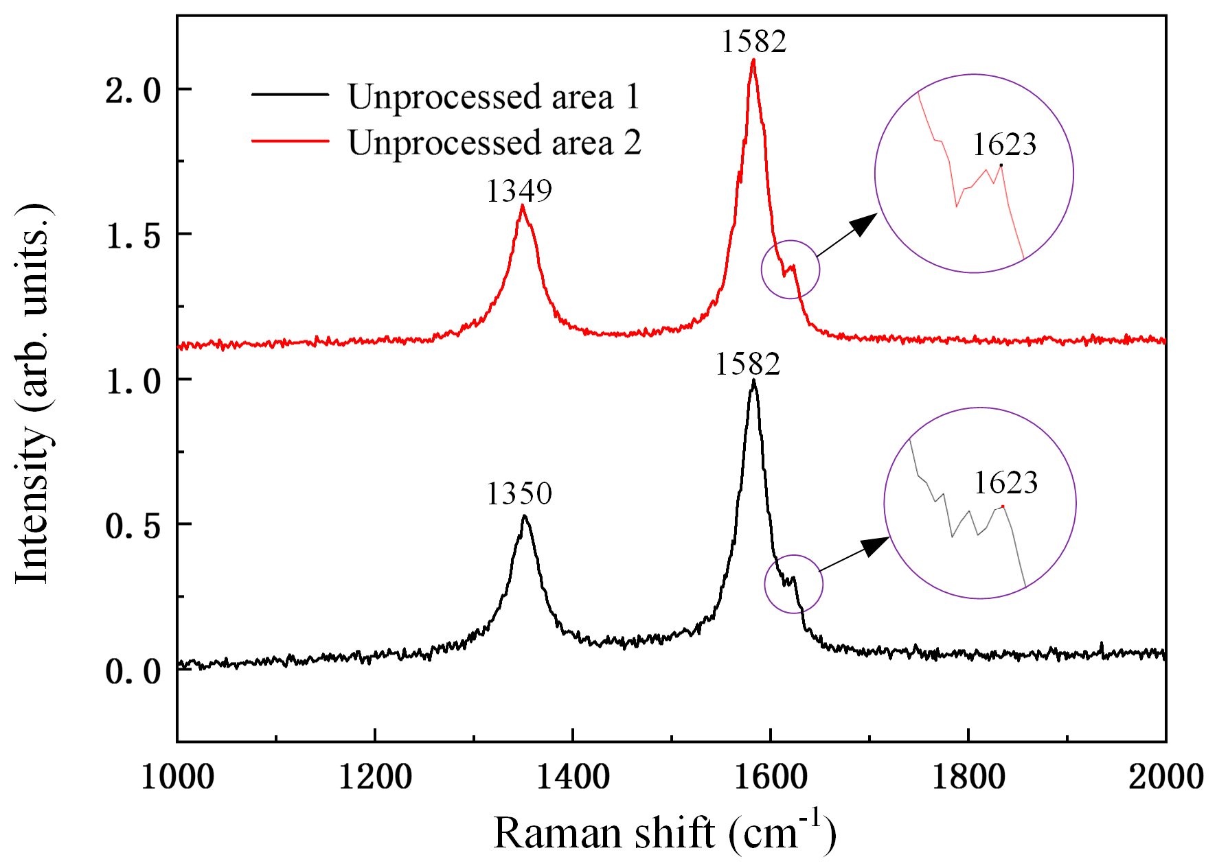
Raman spectroscopy is a crucial technique for the characterization of materials such as graphene and CNTs. It can be used to probe the interactions between the polymer chains and the nanotubes in carbon-based composites, because Raman scattering is resonantly enhanced and induces strong bands in a polymer matrix. Therefore, SEM images and Raman spectroscopy are effective methods for analyzing the structural changes of CNTs after femtosecond laser processing. First, we performed Raman spectroscopy on different areas of the unprocessed material and obtained their Raman spectrum, as shown in Figure 6. Sometimes under certain irradiation conditions, the bands in Raman spectra are affected by carbon deposition in the atmosphere. But in this paper, the Raman characteristic band is the area ratio after peak fitting, so we ignored the carbon deposition in the laser-induced air [31].
CNT film is a typical carbon material formed by stacking CNTs, and the CNTs are formed by curling different layers of graphene. In order to determine the uniformity of the material, the Raman spectra of unprocessed CNT film of composites irradiated are displayed in Figure 6. There were two typical Raman characteristic bands: The D band was around 1350 cm−1, and a high frequency shoulder of the D’ band was located around 1623 cm−1 [32]. Though the two characteristic bands were all double resonance processes, the two characteristic bands were formed in different ways. The degree of defects in CNT films was reflected in their Raman D and D’ bands. The D’ band appeared on the right side of the G band, and the intensity was slightly lower than D band [33]. The characteristic G band formed as a single resonance process was located near 1582 cm−1. The intensity of the G band was correlated with the thickness of the detected CNT films, and the ratio of the D band to the G band () could characterize the defect density.
At different positions of the sample, the D band of 1350 cm−1 appeared to reflect the defects and disorder of CNTs. Compared with the highly oriented pyrolytic graphite (HOPG), the G band had no Raman shift. Therefore, the information of Raman spectral characteristic showed a certain amount of CNTs. The typical characteristic bands D and G were fitted by the least-squares method using the Lorentz line, and the relative area ratio was between 0.5 and 0.52. This indicates that, although the CNT film had certain defects, the uniformity of the CNT film was good. It was observed by SEM that there were many CNTs coated with binders on the surface of the CNT film, which is consistent with the results obtained by Raman spectroscopy.
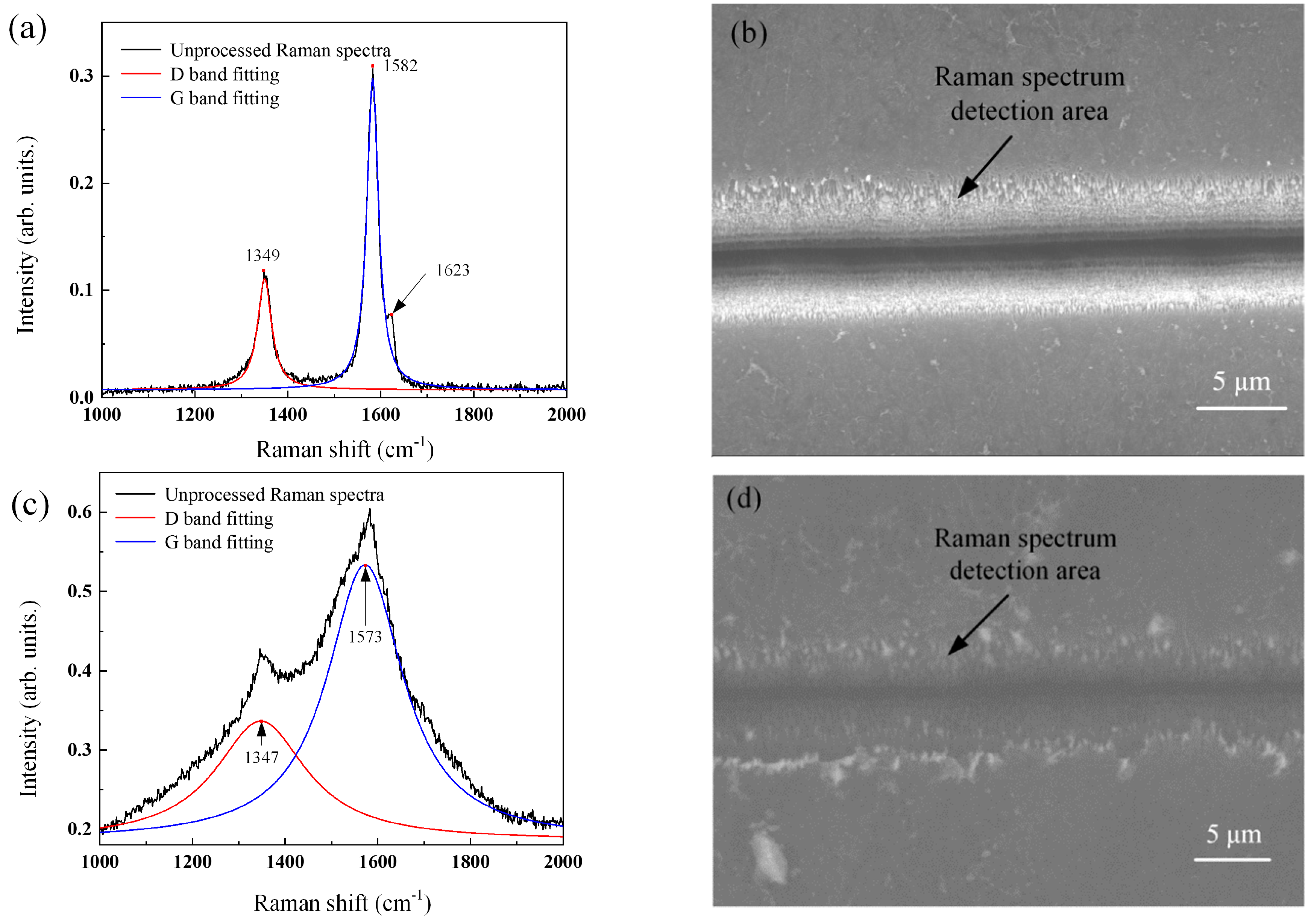
In the cutting process, the photon energy of the short wavelength was higher than that of the long wavelength under the same pulse energy and spot size, so the laser with shorter wavelength had more energy to remove the material. Additionally, the CNT film absorbed more laser light with a shorter wavelength [34]. Therefore, a femtosecond laser with λ = 515 nm and λ =1030 nm was selected to analyze the effect of wavelength on cutting quality. The other parameters were: A pulse duration of 300 fs, a repetition frequency of 40 kHz, a pulse energy of 100 nJ, and a scanning speed of 0.1 mm/s (The polarization direction of the laser was perpendicular to the laser scanning direction). The Raman spectra and SEM topographies are shown in Figure 7. When the pulse energy was low, the Raman spectrum showed that the intensity of the D band did not change much, but the intensity of the G band increased significantly when the laser was processed with a wavelength of 515 nm. The intensity of the D band and the G band increased simultaneously at the wavelength of 1030 nm. The relative area ratio was 0.42 and 0.48, respectively.
Through the irradiation of the femtosecond laser, the composition of the material underwent specific changes. The binder in the CNT film is preferentially ablated by the laser, exposing the CNTs wrapped therein, and the film cutting region was detected as a plurality of the CNT layer with a certain inclination angle. Thus, the intensity of the G band increased. The microscopic topography of the SEM showed a clear cutting groove and no damage on the surface of the film. Therefore, a wavelength of 515 nm could cut the CNT film without damaging the substrate material, and the degree of defect of the display material of the Raman spectrum did not change much.
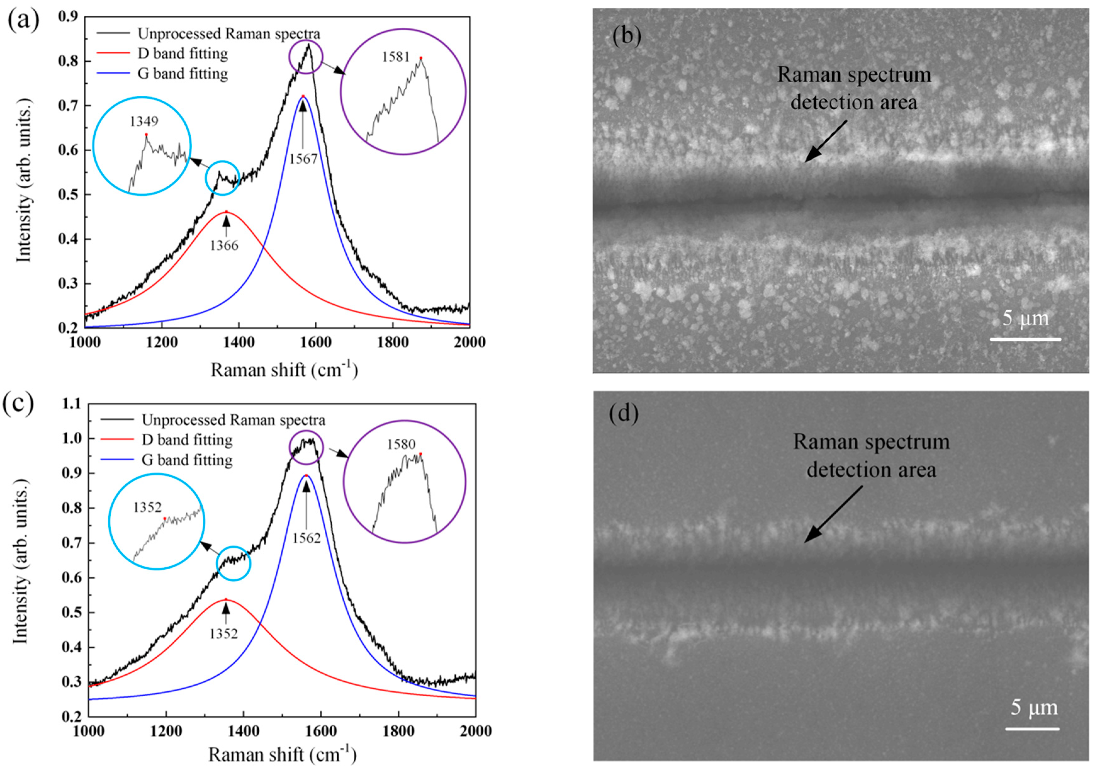
When the wavelength was increased to 1030 nm, the energy of a photon was lower than that of a photon at short wavelength. Under the same parameters, unbroken CNTs existed in the groove after laser cutting, and the edge of the slit was partially detached from the substrate due to the pulsed laser-induced thermal elastic force [35]. The CNT film could not be completely cut, and the cutting edge quality was poor with these processing parameters. Films in this case may cause short circuits if used as microelectrodes. When the laser pulse energy was increased to E = 500 nJ, the intensity and half-width of the D band and G band increased significantly. The D band shifted to higher wavenumbers after Lorentz fitting, and the G band shifted to lower wavenumbers, as shown in Figure 8. The relative area ratios were 0.73 and 0.68, respectively.
The original structures of CNT films was dramatically changed by irradiation with a high laser energy. The increase of D band intensity and band width at half height indicates that the quality of the CNTs was decreased and amorphous carbon existed [36]. The combination of laser induced material vaporization and air breakdown to form a plasma generated a driving force that resulting in tensile deformation of the CNTs—the Raman D band approached 1366 cm−1. There were many CNTs with different degrees of tension in the Raman collection area, which proves that the bond of SP2 hybridization underwent considerable distortion. The G band shifted slightly to lower wavenumbers caused by the tensile deformation of CNTs [37]. A higher femtosecond laser energy caused damage to the substrate material and coagulated on the CNT film at the same time, which changed the lifetime of scattered phonons during G band generation, resulting in an increase in band width at half height and an increase in the acromion strength of the G band.
A large number of recrystallized particles were on the surface of CNT film and in the groove through the micro-morphology, as shown in Figure 8. The processing quality dropped sharply, so laser parameters were no longer suitable for cutting CNT film materials.
3.3.2. Influence of Laser Parameters on Processing Quality
It can be seen from the above analysis that relatively a good quality can be obtained at the wavelength of 515 nm when the other parameters are the same. As such, the wavelength of 515 nm was selected as the further experimental parameter.
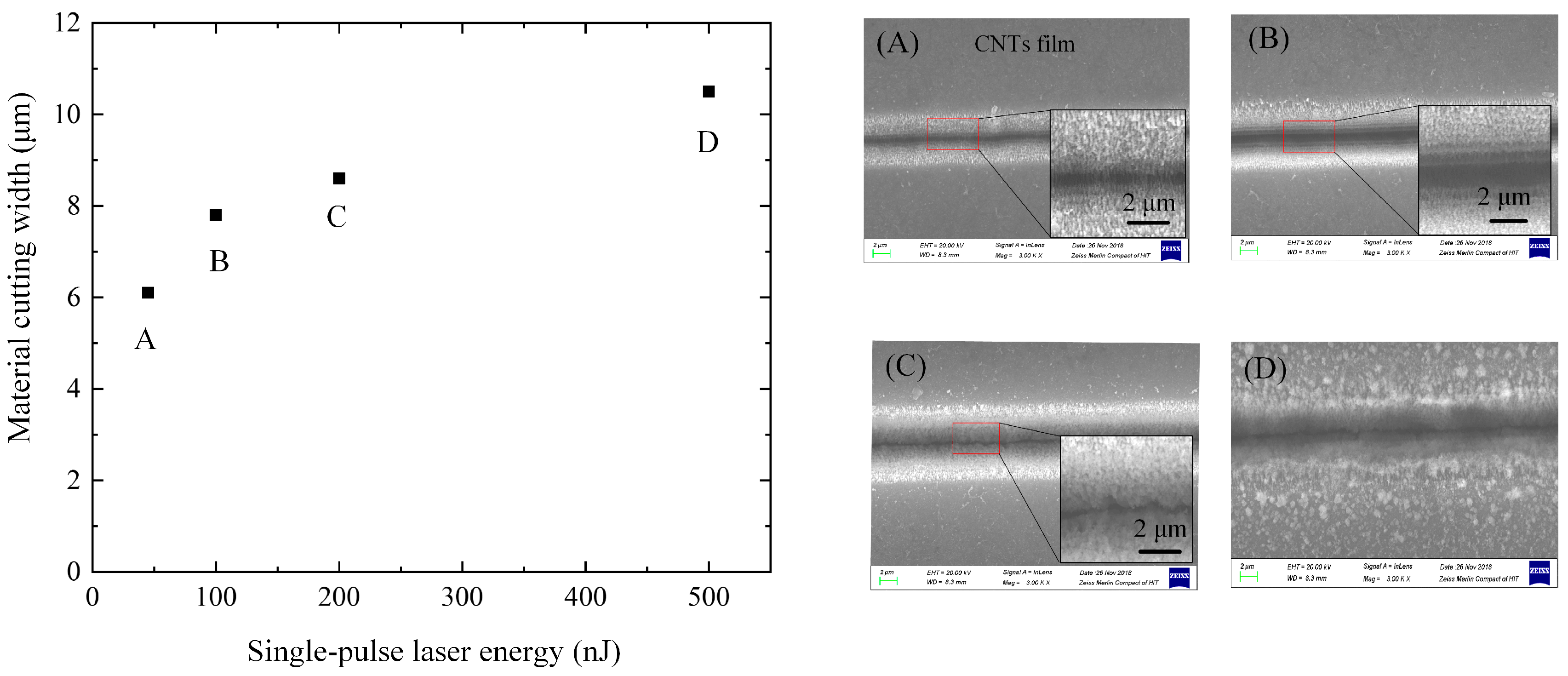
Laser energy was the most critical factor affecting the material cutting, so pulse energies of 45, 100, 200 and 500 nJ were selected to cut the CNT film. The other parameters were a pulse duration of 300 fs, a repetition frequency of 40 kHz, and a scanning speed of 0.1 mm/s. The SEM results are shown in Figure 9.
The groove width increased with the increasing pulse energy, as shown in Figure 9. The cutting edges of CNT film were clean at the pulse energy of 45 nJ, but some CNT filaments were not entirely broken. When the pulse energy is 100 nJ, the cutting groove was smooth and the CNT film was wholly cut off with no apparent CNT filaments. When the pulse energy increased to 200 nJ, there was a large amount of condensate in the groove, the width of the groove bottom became smaller, and re-condensed particles could be observed on the cutting edge, which reduced the cutting quality. At the pulse energy of 500 nJ, the quality of the cut edge deteriorated and a large amount of recompensed matter was simultaneously generated on the surface of the film. Thus far, this parameter was not suitable for cutting.
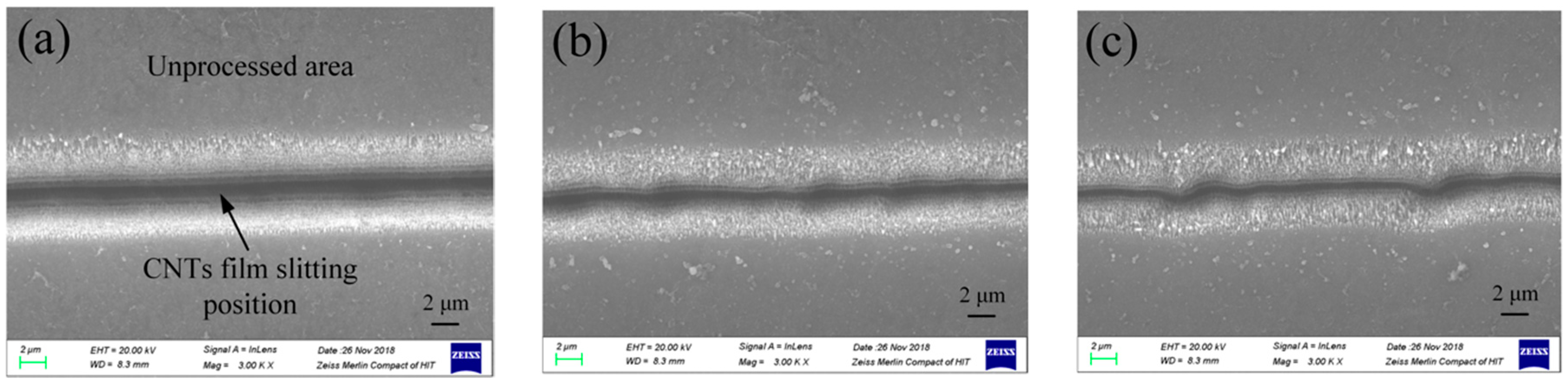
The laser scanning speed is also an essential factor affecting the absorption of energy per unit area of the film. High-quality cutting could be obtained when the pulse energy was 100 nJ and the scanning speed was 0.1 mm/s. The cutting quality decreased, the cutting groove became uneven, and the straightness decreased as the laser scanning speed increased to 1.0 mm/s. The reason for this was the reduction in the number of pulses acting on a unit area and the overlap rate of adjacent pulses, which affected the cutting of the CNT film, resulting in an irregular groove, as shown in Figure 10. The method of increasing the repetition frequency and the scanning speed in equal proportions can be used to improve processing efficiency without influencing processing quality. When the laser scanning parameters of laser frequency was in the range from 40 kHz to 1 MHz and the laser scan speed was from 0.1 mm/s to 1.3 mm/s, the uniformity and straightness of the machined grooves did not change much. Due to the vibration of the moving platform, the straightness decreased after the laser speed exceeded 1.3 mm/s, resulting in a low processing quality.
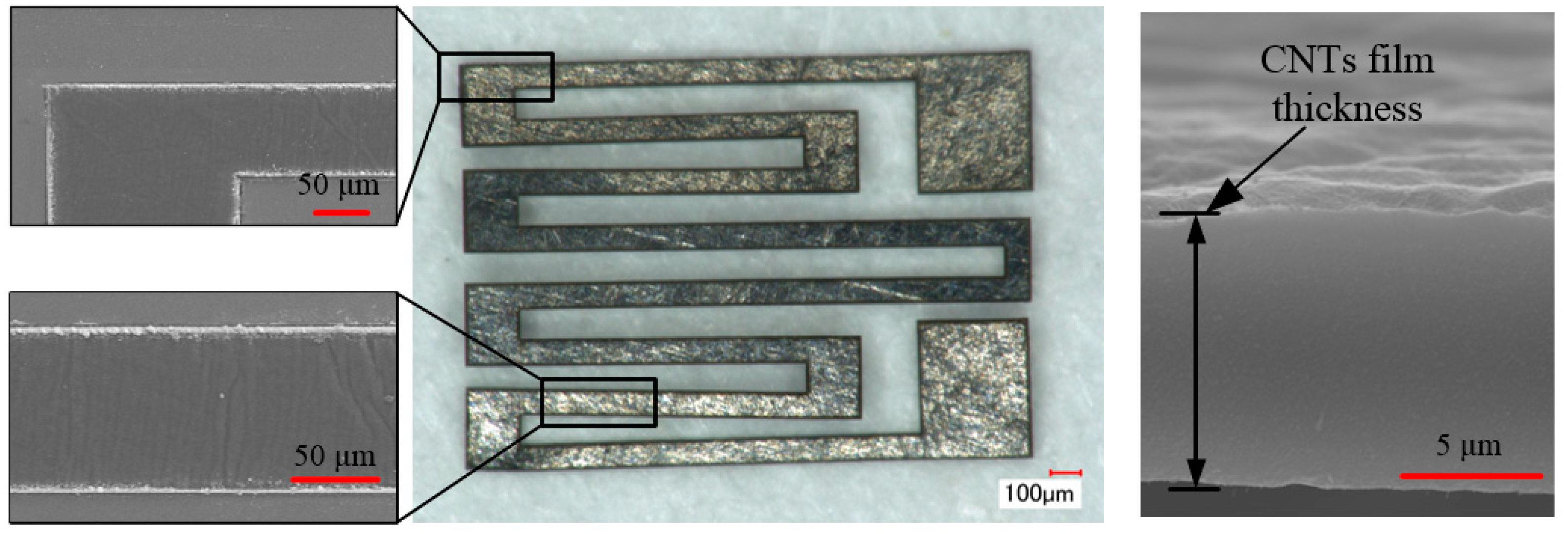
In summary, the processing quality in the femtosecond laser cutting of CNT film first increased and then decreased with the increasing laser pulse energy. The pulse energy of 100 nJ and laser scanning speed of 0.1 mm/s were selected to pattern microstructures on the CNT film. The pattern morphologies were investigated in detail by SEM, as shown in Figure 11. The results exhibited a fine line curve and even area in the patterned region, both of which demonstrate a method of fabricating a film structure to provide a feasible means for the fabrication of integrated circuits [38] and CNT film transistors [39].
4. Conclusions
A method for the ablation of CNT film using a femtosecond laser direct patterning was investigated. The research results of the influence of process parameters on the ablation and patterning show that different pulse energies cause different degrees of ablation of bonded oligomers and CNTs, from surface damage and the reaming of the hole edges to CNTs throwing out due to the ultra-short-pulse laser action. An analysis of the machined CNT film using Raman spectroscopy and SEM showed that the large pulse energy caused defects of the CNT film, the Raman D band intensity increased and shifted to the higher wavenumbers, and the pulsed laser induced thermal elastic force caused a tensile deformation of the film. The parameters of a wavelength of 515 nm, a pulse repetition rate of 40 kHz, a pulse energy of 100 nJ, and a cutting speed of 0.1 mm/s were obtained after optimization without defects or damage on the substrate. The adaptability of this method to be able to machine CNT film on flexible and complex substrates of varying materials, as well as its simplicity and effectiveness, will surely provide technical support for the application of CNT film to electrodes and flexible electronic devices.
Author Contributions
Conceptualization, X.W. and H.Y.; formal analysis, H.Y. and Q.L.; investigation, X.W. and Q.L.; resources, Q.L.; writing—original draft preparation, H.Y.; writing—review and editing, X.W., H.Y. and Q.L.; supervision, X.W.; project administration, X.W.
Acknowledgments
This work was financially supported by the National Key Research and Development Program of China (Grant No. 2018YFB1107600), Basic Research Projects of the “Science and Technology Talents” Program (LGYC2018JC042).
Conflicts of Interest
The authors declare no conflict of interest.
References
- Iijima, S. Helical microtubules of graphitic carbon. Nature 1991, 354, 56–58. [Google Scholar] [CrossRef]
- Cao, A.; Dickrell, P.L.; Sawyer, W.G.; Ghasemi-Nejhad, M.N.; Ajayan, P.M. Super-Compressible Foamlike Carbon Nanotube Films. Science 2005, 310, 1307–1310. [Google Scholar] [CrossRef] [PubMed] [Green Version]
- Wang, Y.; Di, C.; Liu, Y.; Kajiura, H.; Ye, S.; Cao, L.; Wei, D.; Zhang, L.; Li, Y.; Noda, K. Optimizing Single-Walled Carbon Nanotube Films for Applications in Electroluminescent Devices. Adv. Mater. 2010, 20, 4442–4449. [Google Scholar] [CrossRef]
- Liu, J.; Mirri, F.; Notarianni, M.; Pasquali, M.; Motta, N. High performance all-carbon thin film supercapacitors. J. Power Sources 2015, 274, 823–830. [Google Scholar] [CrossRef] [Green Version]
- Cui, K.; Maruyama, S. Multifunctional graphene and carbon nanotube films for planar heterojunction solar cells. Prog. Energy Combust. Sci. 2019, 70, 1–21. [Google Scholar] [CrossRef]
- Xing, Z.; Zhao, J.; Shao, L.; Xiao, H.; Liu, T.; Cui, Z. Highly flexible printed carbon nanotube thin film transistors using cross-linked poly(4-vinylphenol) as the gate dielectric and application for photosenstive light-emitting diode circuit. Carbon 2018, 133, 390–397. [Google Scholar] [CrossRef]
- Hu, D.; Gong, W.; Di, J.; Li, D.; Li, R.; Lu, W.; Gu, B.; Sun, B.; Li, Q. Strong graphene-interlayered carbon nanotube films with high thermal conductivity. Carbon 2017, 118, 659–665. [Google Scholar] [CrossRef]
- Gbordzoe, S.; Yarmolenko, S.; Kanakaraj, S.; Haase, M.R.; Alvarez, N.T.; Borgemenke, R.; Adusei, P.K.; Shanov, V. Effects of laser cutting on the structural and mechanical properties of carbon nanotube assemblages. Mater. Sci. Eng. B 2017, 223, 143–152. [Google Scholar] [CrossRef]
- Bobrinetskiy, I.I.; Emelianov, A.V.; Otero, N.; Romero, P.M. Ultrafast graphene and carbon nanotube film patterning by picosecond laser pulses. In Proceedings of the SPIE International Society for Optics and Photonics on Laser-based Micro-and Nanoprocessing X, San Francisco, CA, USA, 13–18 February 2016; Volume 9736. [Google Scholar]
- Castro, M.; Lasagni, A.; Schmidt, H.; Mücklich, F. Direct laser interference patterning of multi-walled carbon nanotube-based transparent conductive coatings. Appl. Surf. Sci. 2008, 254, 5874–5878. [Google Scholar] [CrossRef]
- Abdelmalek, A.; Bedrane, Z.; Amara, E.-H.; Sotillo, B.; Bharadwaj, V.; Ramponi, R.; Eaton, S.M. Ablation of Copper Metal Films by Femtosecond Laser Multipulse Irradiation. Appl. Sci. 2018, 8, 1826. [Google Scholar] [CrossRef]
- Jing, C.; Wang, Z.; Cheng, Y. Characteristics and Applications of Spatiotemporally Focused Femtosecond Laser Pulses. Appl. Sci. 2016, 6, 428. [Google Scholar] [CrossRef]
- Zhu, D.; Yan, J. Femtosecond Pulse Laser Near-Field Ablation of Ag Nanorods. Appl. Sci. 2019, 9, 363. [Google Scholar] [CrossRef]
- Terakawa, M. Femtosecond Laser Processing of Biodegradable Polymers. Appl. Sci. 2018, 8, 1123. [Google Scholar] [CrossRef]
- Cui, J.; Cheng, Y.; Zhang, J.; Mei, H.; Wang, X. Femtosecond Laser Irradiation of Carbon Nanotubes to Metal Electrodes. Appl. Sci. 2019, 9, 476. [Google Scholar] [CrossRef]
- Serien, D.; Kawano, H.; Miyawaki, A.; Midorikawa, K.; Sugioka, K. Femtosecond Laser Direct Write Integration of Multi-Protein Patterns and 3D Microstructures into 3D Glass Microfluidic Devices. Appl. Sci. 2018, 8, 147. [Google Scholar] [CrossRef]
- Alnaser, A.S.; Khan, S.A.; Ganeev, R.A.; Stratakis, E. Recent Advances in Femtosecond Laser-Induced Surface Structuring for Oil–Water Separation. Appl. Sci. 2019, 9, 1554. [Google Scholar] [CrossRef]
- Yoon, J.-W.; Chang, W.S.; Cho, S.H. Laser direct patterning of AgNW/CNT hybrid thin films. Opt. Lasers Eng. 2015, 73, 40–45. [Google Scholar] [CrossRef]
- Yoon, J.-W.; So, H.-M.; Cho, S.-H.; Chang, W.S. Effect of polarization of ultrafast laser irradiation on carbon nanotube film. Thin Solid Film. 2013, 546, 69–72. [Google Scholar] [CrossRef]
- Kalita, G.; Qi, L.; Namba, Y.; Wakita, K.; Umeno, M. Femtosecond laser induced micropatterning of graphene film. Mater. Lett. 2011, 65, 1569–1572. [Google Scholar] [CrossRef]
- Colomer, J.-F.; Stephan, C.; Lefrant, S.; Van Tendeloo, G.; Willems, I.; Kónya, Z.; Fonseca, A.; Laurent, C.; Nagy, J. Large-scale synthesis of single-wall carbon nanotubes by catalytic chemical vapor deposition (CCVD) method. Chem. Phys. Lett. 2000, 317, 83–89. [Google Scholar] [CrossRef] [Green Version]
- Gao, Y.; Marconnet, A.M.; Xiang, R.; Maruyama, S.; Goodson, K.E. Heat Capacity, Thermal Conductivity, and Interface Resistance Extraction for Single-Walled Carbon Nanotube Films Using Frequency-Domain Thermoreflectance. IEEE Trans. Compon. Packag. Manuf. Technol. 2013, 3, 1524–1532. [Google Scholar]
- Wąsik, M.; Dużyńska, A.; Judek, J.; Pawłowski, M.; Świtkowski, K.; Witowski, A.M.; Zdrojek, M. Ultraviolet to far-infrared transmission properties of thin film multi-walled carbon nanotube random networks. J. Mater. Sci. 2017, 52, 3086–3094. [Google Scholar] [CrossRef]
- Spellauge, M.; Loghin, F.-C.; Sotrop, J.; Domke, M.; Bobinger, M.; Abdellah, A.; Becherer, M.; Lugli, P.; Huber, H.P. Ultra-short-pulse laser ablation and modification of fully sprayed single walled carbon nanotube networks. Carbon 2018, 138, 234–242. [Google Scholar] [CrossRef]
- Pino, A.P.; Gyorgy, E.; Hussain, S.; Andujar, J.L.; Pascual, E.; Amade, R.; Bertran, E. Laser-induced nanostructuration of vertically aligned carbon nanotubes coated with nickel oxide nanoparticles. J. Mater. Sci. 2017, 52, 4002–4015. [Google Scholar] [CrossRef]
- Romero, A.H.; Garcia, M.E.; Valencia, F.; Terrones, H.; Terrones, M.; Jeschke, H.O. Femtosecond Laser Nanosurgery of Defects in Carbon Nanotubes. Nano Lett. 2005, 5, 1361–1365. [Google Scholar] [CrossRef]
- Li, X.; Jiang, L.; Tsai, H.-L. Phase change mechanisms during femtosecond laser pulse train ablation of nickel thin films. J. Appl. Phys. 2009, 106, 064906. [Google Scholar] [CrossRef] [Green Version]
- Sohn, I.-B.; Noh, Y.-C.; Choi, S.-C.; Ko, D.-K.; Lee, J.; Choi, Y.-J. Femtosecond laser ablation of polypropylene for breathable film. Appl. Surf. Sci. 2008, 254, 4919–4924. [Google Scholar] [CrossRef]
- Kichambare, P.; Chen, L.-C.; Wang, C.; Ma, K.; Wu, C.; Chen, K. Laser irradiation of carbon nanotubes. Mater. Chem. Phys. 2001, 72, 218–222. [Google Scholar] [CrossRef]
- Ma, R.; Wei, B.; Xu, C.; Liang, J.; Wu, D. The morphology changes of carbon nanotubes under laser irradiation. Carbon 2000, 38, 636–638. [Google Scholar] [CrossRef]
- Grehn, M.; Seuthe, T.; Reinhardt, F.; Hofner, M.; Griga, N.; Eberstein, M.; Bonse, J. Debris of potassium–magnesium silicate glass generated by femtosecond laser-induced ablation in air: An analysis by near edge X-ray absorption spectroscopy, micro Raman and energy dispersive X-ray spectroscopy. Appl. Surf. Sci. 2014, 302, 286–290. [Google Scholar] [CrossRef]
- Bokobza, L.; Bruneel, J.-L.; Couzi, M. Raman spectroscopy as a tool for the analysis of carbon-based materials (highly oriented pyrolitic graphite, multilayer graphene and multiwall carbon nanotubes) and of some of their elastomeric composites. Vib. Spectrosc. 2014, 74, 57–63. [Google Scholar] [CrossRef]
- Bokobza, L.; Bruneel, J.-L.; Couzi, M. Raman spectroscopic investigation of carbon-based materials and their composites. Comparison between carbon nanotubes and carbon black. Chem. Phys. Lett. 2013, 590, 153–159. [Google Scholar] [CrossRef]
- Lin, H.K.; Lin, R.C.; Li, C.H. Etching processes of transparent carbon nanotube thin films using laser technologies. Thin Solid Film. 2010, 518, 7253–7257. [Google Scholar] [CrossRef]
- Joo, M.; Lee, M. High-quality parallel patterning of carbon nanotube thin films by a pulsed laser beam. Thin Solid Film. 2012, 520, 3971–3974. [Google Scholar] [CrossRef]
- Stramel, A.; Gupta, M.; Lee, H.; Yu, J.; Edwards, W. Pulsed laser deposition of carbon nanotube and polystyrene–carbon nanotube composite thin films. Opt. Lasers Eng. 2010, 48, 1291–1295. [Google Scholar] [CrossRef]
- Plotnikov, V.A.; Demyanov, B.F.; Yeliseeyev, A.P.; Makarov, S.V.; Zyryanova, A.I. Structural state of diamond-like amorphous carbon films, obtained by laser evaporation of carbon target. Diam. Relat. Mater. 2018, 91, 225–229. [Google Scholar] [CrossRef]
- Sun, D.-M.; Timmermans, M.Y.; Tian, Y.; Nasibulin, A.G.; Kauppinen, E.I.; Kishimoto, S.; Mizutani, T.; Ohno, Y. Flexible high-performance carbon nanotube integrated circuits. Nat. Nanotechnol. 2011, 6, 156–161. [Google Scholar] [CrossRef]
- De Volder, M.F.L.; Tawfick, S.H.; Baughman, R.H.; Hart, A.J. Carbon Nanotubes: Present and Future Commercial Applications. Science 2013, 339, 535–539. [Google Scholar] [CrossRef] [Green Version]
Figure 1.
The schematic diagram of the experimental setup of the femtosecond laser percussion ablating.
Figure 1.
The schematic diagram of the experimental setup of the femtosecond laser percussion ablating.

Figure 2.
(a) SEM image of carbon nanotube (CNT) film ablated by different laser pulse energies and number of pulses and (b) plot of the diameter square of the produced craters changing with the logarithm of pulse energy.
Figure 2.
(a) SEM image of carbon nanotube (CNT) film ablated by different laser pulse energies and number of pulses and (b) plot of the diameter square of the produced craters changing with the logarithm of pulse energy.

Figure 3.
Ablation morphology at different pulse energies with the number of pulses N = 5, 50, 200.

Figure 4.
Ablation diameter versus number of pulses under different pulse energy conditions indicated in the plot legend.
Figure 4.
Ablation diameter versus number of pulses under different pulse energy conditions indicated in the plot legend.

Figure 5.
(a) Surface morphology of hole under E = 25 nJ ablation; (b) schematic illustration on the ablation mechanism with different pulse energies; and (c) surface morphology of hole under E = 165 nJ ablation. (The direction of double arrows in the figure is the polarization direction of the laser).

Figure 6.
Raman spectra of two unprocessed areas of CNT film.

Figure 7.
Raman detection and SEM image of the groove entrance of CNT film by laser cutting at different wavelengths under a low pulse energy. (a,b) λ = 515 nm; (c,d) λ = 1030 nm.
Figure 7.
Raman detection and SEM image of the groove entrance of CNT film by laser cutting at different wavelengths under a low pulse energy. (a,b) λ = 515 nm; (c,d) λ = 1030 nm.

Figure 8.
Raman detection and SEM image of the groove entrance of CNT film by laser cutting at different wavelengths under high pulse energy. (a,b) λ = 515 nm; (c,d) λ = 1030 nm.
Figure 8.
Raman detection and SEM image of the groove entrance of CNT film by laser cutting at different wavelengths under high pulse energy. (a,b) λ = 515 nm; (c,d) λ = 1030 nm.

Figure 9.
SEM images of CNT film ablation grooves with different single pulse energies (A) E = 45 nJ; (B) E = 100 nJ; (C) E = 200 nJ; (D) E = 500 nJ.
Figure 9.
SEM images of CNT film ablation grooves with different single pulse energies (A) E = 45 nJ; (B) E = 100 nJ; (C) E = 200 nJ; (D) E = 500 nJ.

Figure 10.
Different laser scanning speeds of the cutting morphology of the CNT film (a) v = 0.1 mm/s; (b) v = 0.5 mm/s; and (c) v = 1.0 mm/s.
Figure 10.
Different laser scanning speeds of the cutting morphology of the CNT film (a) v = 0.1 mm/s; (b) v = 0.5 mm/s; and (c) v = 1.0 mm/s.

Figure 11.
Femtosecond laser processing of self-supporting CNT film placed on optical microscope display platform microstructure image. (The local enlargement part is the SEM image.).
Figure 11.
Femtosecond laser processing of self-supporting CNT film placed on optical microscope display platform microstructure image. (The local enlargement part is the SEM image.).

© 2019 by the authors. Licensee MDPI, Basel, Switzerland. This article is an open access article distributed under the terms and conditions of the Creative Commons Attribution (CC BY) license (http://creativecommons.org/licenses/by/4.0/).
Share and Cite
MDPI and ACS Style
Wu, X.; Yin, H.; Li, Q. Ablation and Patterning of Carbon Nanotube Film by Femtosecond Laser Irradiation. Appl. Sci. 2019, 9, 3045. https://0-doi-org.brum.beds.ac.uk/10.3390/app9153045
AMA Style
Wu X, Yin H, Li Q. Ablation and Patterning of Carbon Nanotube Film by Femtosecond Laser Irradiation. Applied Sciences. 2019; 9(15):3045. https://0-doi-org.brum.beds.ac.uk/10.3390/app9153045
Chicago/Turabian StyleWu, Xuefeng, Hailiang Yin, and Qiang Li. 2019. "Ablation and Patterning of Carbon Nanotube Film by Femtosecond Laser Irradiation" Applied Sciences 9, no. 15: 3045. https://0-doi-org.brum.beds.ac.uk/10.3390/app9153045
Note that from the first issue of 2016, this journal uses article numbers instead of page numbers. See further details here.