Article

Understanding the Origin of the Hysteresis of High-Performance Solution Processed Polycrystalline SnO2 Thin-Film Transistors and Applications to Circuits

Display Research Center, Department of Information Display, Kyung Hee University, Seoul 02447, Korea
*
Author to whom correspondence should be addressed.
Submission received: 31 October 2021 / Revised: 30 November 2021 / Accepted: 16 December 2021 / Published: 22 December 2021
(This article belongs to the Special Issue Thin-Film Transistors)

Abstract

:
Crystalline tin oxide has been investigated for industrial applications since the 1970s. Recently, the amorphous phase of tin oxide has been used in thin film transistors (TFTs) and has demonstrated high performance. For large area electronics, TFTs are well suited, but they are subject to various instabilities due to operating conditions, such as positive or negative bias stress PBS (NBS). Another instability is hysteresis, which can be detrimental in operating circuits. Understanding its origin can help fabricating more reliable TFTs. Here, we report an investigation on the origin of the hysteresis of solution-processed polycrystalline SnO2 TFTs. We examined the effect of the carrier concentration in the SnO2 channel region on the hysteresis by varying the curing temperature of the thin film from 200 to 350 °C. Stressing the TFTs characterized further the origin of the hysteresis, and holes trapped in the dielectric are understood to be the main source of the hysteresis. With TFTs showing the smallest hysteresis, we could fabricate inverters and ring oscillators.

1. Introduction

With the development of amorphous oxide semiconductor (AOS) electronics, various oxide-based semiconductors have been investigated. Indium gallium zinc oxide (IGZO) [1], indium zinc oxide (IZO) [2], indium gallium oxide (IGO) [3], zinc tin oxide (ZTO) [4], and indium zinc tin oxide (IZTO) [5] all have in common an amorphous phase, a conduction through s orbitals, optical transmittance of ~80% in the visible region, and offer a mobility of ~10 cm2/Vs [1].
Single cation-based oxides demonstrate a polycrystalline phase with higher mobilities. Zinc oxide (ZnO) [6], indium oxide (In2O3) [3], and tin oxide (SnO2) [7] are among the most investigated materials. One of the most valuable metrics in TFTs is the mobility, and ZnO TFTs have demonstrated 40–70 cm2/Vs [6,8] while In2O3 TFTs [4] have demonstrated mobilities ~50 cm2/Vs. Even the crystalline form of IGZO (c-axis crystalline IGZO, the so called CAAC-IGZO) has attracted attention due to the TFTs reaching mobilities ~90 cm2/Vs [9,10]. For a few years now, tin oxide has regained attention. Devices comprising SnO2 have demonstrated high mobility. Perovskite solar cells [11,12] and TFTs have been the main focus of research. TFTs have shown mobilities ranging from 40 to 147 cm2/Vs [13,14]. Even more recently, the amorphous phase of tin oxide [15,16] has demonstrated possible use in TFTs, reaching similar performances as the polycrystalline counterpart. Interestingly, in all these studies authors used a high-k dielectric as the gate insulator (ZrO2, HfO2, Al2O3), and a very thin channel layer (less than 10 nm).
With the use of high-k dielectrics [17], it is possible to obtain clockwise or anticlockwise hysteresis in the TFTs. The reasons are multiple, but shortly, in n-type based TFTs, the clockwise hysteresis can be resulting from the semiconductor (trapping of the electrons), while the anticlockwise from the gate dielectric (due to the movement of mobile ions for example) [18]. The anticlockwise behavior can be used in memory devices, while it can be detrimental for circuits. To fully understand the origin of the hysteresis (i.e., trapping of charge carriers, movement of mobile ions in the semiconductor or in the dielectric), measuring the hysteresis at slow and fast rates can help discriminate the origin.
We previously demonstrated that solution processed SnO2 using SnCl2 precursors could have various phases, and that the curing and annealing temperatures could impact significantly the various optical, electrical, and physical properties [19]. Here, we implemented the polycrystalline SnO2 thin films fabricated at various Tcuring temperatures (200, 280, and 350 °C) and a fixed annealing temperature (Tanneal = 350 °C). High mobility TFTs (over 100 cm2/Vs) are obtained and we studied the hysteresis behaviors of the polycrystalline SnO2 TFTs (poly-SnO2 TFTs). By varying the sweep rate and applying negative and positive bias stresses to the TFTs, we can clearly identify the origin of the hysteresis.

2. Materials and Methods

2.1. Fabrication of the Precursor Solutions

Solutions of HfO2 (SnO2) were made by mixing HfCl4 (SnCl2) into a mixture of acetonitrile (Ac) and ethyleneglycol (Etg). We used 35% of Ac and 65% of Etg in volume%. The HfO2 (SnO2) precursor solutions were stirred in a N2 environment for 2 h (24 h) before use. The HfO2 precursor solutions had a concentration of 0.2 M and the SnO2 ones had a concentration of 0.2 M for the thin films, and 0.167 M for the TFTs.

2.2. Thin Film Fabrication and Analysis

The SnO2 thin films were fabricated by spin-coating at 2000 rpm during 25 s. After spin-coating, the layer was subject to a curing at 100 °C for 5 min, and a second curing step at 200, 280, or 350 °C for 5 min. The coating was repeated once. We measured the Hall effect on a Ecopia HMS-3000. The samples had a van der Pauw configuration. The data was collected from 15 points. We used the Kα line (1.54 Å) for X-ray diffraction measurement to evaluate the crystallinity of the thin films. The surface roughness was evaluated by atomic force microscopy (AFM) by using a XE-7 from Park systems. The optical properties were evaluated by using an Scinco S4100. We measured X-ray photospectroscopy (XPS) with a Nexsa from ThermoFisher Scientific, by using the Al-Ka at 1486.6 eV as the X-ray source. Calibration was made with the carbon peak at 284.8 eV.

2.3. Thin Film Transistor Fabrication and Analysis

We fabricated poly-SnO2 TFTs by first sputtering 40 nm Mo as the gate on glass. After patterning, we spin-coated the HfO2 film. The coating was made at 2000 rpm for 25 s. The layer was then subject to a curing at 250 °C for 5 min, and UV treatment during 90 s. The deposition, curing, and treatment were repeated to obtain a 95 nm thick HfO2 layer. The samples were then subject to annealing at 350 °C for 2 h in air. The precursor solution of SnO2 was spin-coated at 4000 rpm during 25 s, and followed a curing step explained in the previous paragraph. After patterning, the TFTs were annealed at 350 °C for 2 h in air. We created via holes, sputtered and patterned IZO as the source/drain electrodes. Finally, a hot-plate annealing at 300 °C for 2 h and another hot-plate annealing step at 350 °C for 1 h were performed.
We measured the TFTs IV curves with a 4156 C semiconductor parameter analyzer. The TFTs had a width W and a length L of 50 and 10 μm, respectively. We evaluated the field-effect mobility in the linear region
μ lin = I DS V GS | V DS = 0.1 V × L / ( V DS × W × Cox )
where Cox is the HfO2 capacitance.
The threshold voltage was evaluated at W/L × 10−10 A. The slope was evaluated as
S . S . = V GS l o g I DS .
The various parameters were averaged over 25 TFTs. The various parameters are extracted from the transfer curve measured at fast measurement rate, from negative to positive voltage. The hysteresis was measured at VDS = 0.1 V, with a fast and a slow measurement rate related to an integration time of 6.04, and 20 ms, respectively. The positive (negative) bias stress PBS (NBS) were measured by applying VGS = 3 V (−3 V) during 1 h. We note that the capacitance of the hafnium oxide dielectric was 219 nF/cm2 [15].

2.4. Circuit Fabrication

The inverter and ring oscillator followed the same process steps as the TFTs. The inverter had a load TFT with width and length of 50 and 6µm, respectively. The driving TFT had a width and length of 400 µm and 6 µm. The inverter had a depletion mode structure with the gate of the load TFT connected to the output.
The ring oscillator consisted of 11 of these inverters. The output of one is connected as the input of the following one. The last inverter being connected to the first inverter. A buffer inverter is put at the end of the ring oscillator to stabilize the measured output.

3. Results

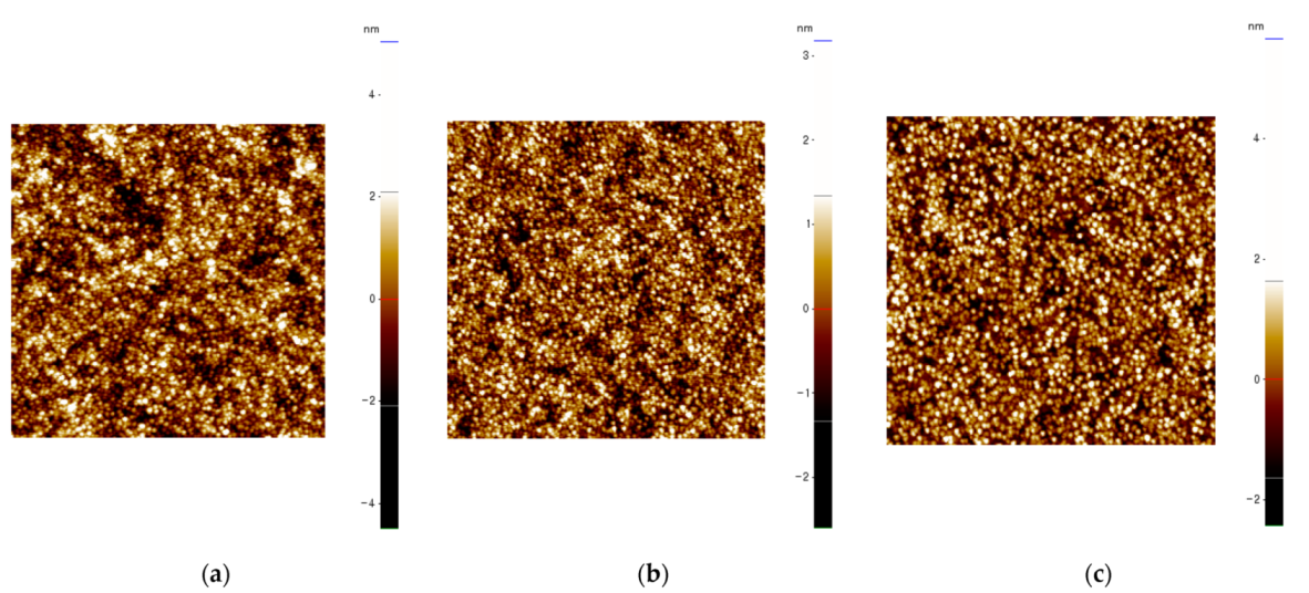
3.1. Thin Film Analysis

Figure 1 shows the optical and crystalline properties of SnO2. Figure 1a shows the extraction of the band gap from the Tauc plot [20]. The films with a Tcuring of 200, 280, and 350 °C had a respective bandgap of 3.89, 3.94, and 3.94 eV. The films are adequate for application in invisible electronics [1]. Figure 1b shows the results of the XRD measurements. For all Tcuring, the thin films demonstrate the crystalline structure. Peaks related to the (110), (101), (200), and (211) are all observed. They are located at 26.6°, 33.8°, 37.8°, and 51.8°, respectively, for the thin film with the Tcuring of 280 °C.
We extracted the carrier concentration N and the Hall mobility µH according to their definition:
µ H = | R H | ρ  
N   = 1 / ( R H e )
where RH is the Hall coefficient, and ρ the electrical resistivity.
For the SnO2 film cured at 200, 280, and 350 °C, we observe an increase in the carrier concentration from 1.37 ± 0.19 to 4.28 ± 0.54 to 4.47 ± 1.20 × 1018 cm−3. The Hall mobility also increases from 1.56 ± 0.32 to 1.79 ± 0.67 and to 2.28 ± 0.92 cm2/Vs. The mobility increases with the carrier concentration as for oxide semiconductors which has been explained by the percolation conduction of the charge carriers [21]. Also, we note that the values match the trend previously reported for SnO2 [19].
Figure 2 shows the surface morphologies of SnO2 made at the different curing temperatures measured by AFM. The quality of the surface can be assessed by two metrics: the root mean square roughness (Rrms) and also the peak-to-valley roughness (Rpv). The respective Rrms roughness of SnO2 cured at 200 (Figure 2a), 280 (Figure 2b), and 350 °C (Figure 2c) were 1.074, 0.725, and 0.844 nm and their respective Rpv values were 9.522, 5.778, and 8.092 nm. Therefore, curing SnO2 at 280 °C (Figure 2b) leads to the smoothest surface. We note that we observe the crystallite sizes were in the 10–25 nm range, with the biggest crystallites for the 350 °C cured film. We note that the roughnesses decrease then increase at 280 °C. This was previously reported to be due to the melting of SnCl2 at 250 °C [19], which would alter the crystallization of the 280 °C-cured thin films leading to a smoother surface.

3.2. Thin Film Transistor and the Origin of Their Hysteresis

The typical poly-SnO2 TFT structure used in this work is shown at the bottom of Figure 3a. The micrograph of the TFT shown on top of Figure 3a reveals the various elements constituting the TFT. The hysteresis of the TFT transfer curves measured at fast and low rates, when SnO2 was cured at 200, 280, and 350 °C are shown in Figure 3b–d, respectively. On average the TFTs made with a SnO2 thin film cured at 200, 280, and 350 °C show a linear mobility of 86 ± 12, 90 ± 12, 110 ± 35 cm2/Vs; a Vth of −0.04 ± 0.05, 0.02 ± 0.12, −0.19 ± 0.14 V; and a subthreshold swing of 103.7 ± 9.9, 112.9 ± 9.4, and 102.7 ± 8.4 mV/dec. We note that the reliability of the extraction of the mobility in particular is highly depending on the size of the TFT [22]. The size chosen in the study should not have a significant impact on the mobility value [15,22]. We gather in Table 1 our present results and various other TFT performances using polycrystalline oxide semiconductors.
We note that even though the hysteresis is an important parameter, the characterization is only seldom reported.
At the Tcuring of 200 and 280 °C, the hysteresis is clockwise, and the slow sweep rate measurements lead to higher hysteresis than the fast sweep rate measurements. We note that the slow sweep rate hysteresis for the 280 °C-cured-SnO2 is smaller than the TFTs with the 200 °C-cured-SnO2 layer. Also, the fast sweep measurement rate leads to a ~0.15 V hysteresis. At Tcuring of 350 °C, an anticlockwise hysteresis is observed, and the fast sweep rate leads to higher hysteresis than the slow sweep rate. The reason why the TFT only shows the anticlockwise hysteresis will be discussed later.
A slow mobility species or a slow phenomenon responsible for the hysteresis for the 200- and 280 °C cured SnO2 based TFT could be the reason for the slow sweep measurement rate leading to higher hysteresis than the fast measurement rate [18]. Also, the amount of the species would be smaller in the former than the later. The anticlockwise hysteresis is usually resulting from moving ions in the dielectric, from charge carriers entering the dielectric, or from the polarization of the dielectric. An anticlockwise hysteresis resulting from the polarization of the dielectric would have appeared in all conditions, and cannot therefore explain the behavior of our TFTs. Also, a clockwise hysteresis usually results from charge carriers near/at the channel/dielectric interface. To clarify the underlying phenomenon, we performed PBS and NBS on the TFTs, and measured the hysteresis.

3.3. Bias Stress Effect on Poly-SnO2 Thin-Film Transistors

Figure 4a–f show the variation in the hysteresis under NBS (PBS) for TFT using SnO2 having Tcuring of 200 (Figure 4a,d), 280 (Figure 4b,e), and 350 °C (Figure 4c,f), respectively. As shown in Figure 4a–c, all curves shift negatively under NBS. Interestingly, the direction in the hysteresis changes in the 280 °C-cured SnO2 based TFT from clockwise to anticlockwise (Figure 4b). Besides, the hysteresis becomes close to 0 V for the 200 °C-cured SnO2 TFT. Not only did we consider the change in the transfer curve (the IDS curve), we also considered the evolution of the gate leakage current (the IGS curve). Under NBS, IGS increases by almost an order of magnitude in all TFTs. The anticlockwise hysteresis appearing under NBS suggests that holes could enter the dielectric during the stress.
Figure 4d,e show that the 200- and 280 °C-cured SnO2 TFT have a positive shift and a decrease in the current under PBS. Also, we observe the decrease of IGS in Figure 4d,e. The decrease in the IGS is almost one order of magnitude for the 200 °C-cured TFT. For the 350 °C-cured TFT, we observe that the TFT current decreases without a significant change in the Vth. Therefore, considering the various stresses and the various change in Vth and the change in IGS, we understand that charge carriers are injected from and to the dielectric.
We therefore evaluated the band offsets between SnO2 and HfO2 for all three different curing temperatures of SnO2 [26]. The valence band offset ΔEv is defined as
ΔEv = (EHf4f − EVBM)HfO2surface − (ESn3d5/2 − EVBM)SnO2surface − (EHf4f − ESn3d5/2)SnO2/HfO2,
where HfO2surface, SnO2surface and SnO2/HfO2 denote, respectively, the top of the HfO2 layer without SnO2 on top of it, the top of the SnO2 layer, and the HfO2/SnO2 interface.
Therefore, for each curing temperature we extracted the following peak values: the Hf 4f peak at the SnO2/HfO2 interface (as shown in Figure 5a,e,i), the Sn 3d5/2 peak at the SnO2/HfO2 interface (as shown in Figure 5b,f,j), the Sn 3d5/2 peak on the top of the SnO2 layer (Figure 5c,g,k), and the valence band at the top of the SnO2 layer (as shown in Figure 5d,h,l). The various extracted values are gathered in Table 2. We note that the values for the position peaks taken for HfO2 without SnO2 on top are taken from a previous report [16] and we consider the Hf 4f peak position EHf4f = 18.15 eV, the bandgap of HfO2 EgHfO2 = 5.34 eV, and the position of the valence band EVBM = 2.4 eV.
We could evaluate that the valence band offset was 0.17, 0.19 and 0.09 eV for the 200- 280- and 350 °C-cured SnO2 layer, respectively. To avoid charge carrier injection, the offset value should be bigger than 1 eV [27]. So, our TFTs having a smaller band offset could have holes injected into the dielectric.
The small offset can therefore explain the possibility of holes to be trapped into (detrapped from) the dielectric under NBS (PBS). The presence of trapped holes in the dielectric would add up to the electric field attracting more electrons in the channel resulting in an anticlockwise hysteresis. Under PBS, holes can exit the dielectric leading to a decrease in the gate leakage, but also a decrease in the electron current. Thus, trapping of electrons would lead to the observed clockwise hysteresis.
The fact that only the 350 °C-cured SnO2 TFT demonstrate the anticlockwise hysteresis could result from the higher density of holes in the SnO2 layer compared to the other temperature cured SnO2 layer based TFTs. Also, the TFT cured at 350 °C showed an apparent higher mobility. But this value is certainly due to the presence of injected holes in the gate insulator increasing the electron density in the channel during operation and therefore leading to an increased value of the mobility. We note that the 280 °C-cured-SnO2 layer showing the smallest RRMS and Rpp value leads to the TFT with the smallest clockwise hysteresis. As mentioned before, we previously studied the fabrication of SnO2 thin films at various curing and annealing temperatures [19]. We demonstrated that the melting of the precursors at 250 °C had an impact on the various properties of the thin films. The various films had an increase of the Rrms roughness and RPV for temperatures higher than the melting temperature. The TFT properties are consistent with the thin film fabrication process and their properties.
Also, we note that holes should be moving slowly in SnO2, as they would in IGZO with a mobility of ~0.01 cm2/Vs [28]. Under NBS, holes may be injected from the SnO2 layer to the dielectric and be trapped, resulting in a negative shift and the anticlockwise hysteresis. This also explains the change of the hysteresis direction for the 280 °C-cured SnO2 based TFT shown in Figure 4b. Therefore, we propose that the main phenomenon responsible for the hysteresis in our solution-processed SnO2 TFT is the trapping of holes in the dielectric. Detrapping or trapping of holes would therefore monitor the hysteresis. Figure 6 shows the band offsets between HfO2 and polycrystalline SnO2 Figure 6a summarizes the bandgaps (3.89–3.94 eV for SnO2, 5.34 eV for HfO2), ΔEv (0.09–0.19 eV), and ΔEc (deduced from the previous values). To find ΔEv, we used the values taken from Figure 5, and gathered in Table 2. Figure 6b,c summarize the proposed mechanism of the hole extraction (injection) during PBS (NBS).

3.4. Application to Circuits: Inverters and Ring Oscillators

We fabricated both inverters and ring oscillators as circuits to demonstrate the possibility to incorporate SnO2 TFT in more advanced circuitry. We chose the devices with a curing step at 280 °C. Indeed, the TFTs showed the clockwise hysteresis. Compared to the 200 °C cured TFTs, the 280 °C-cured TFTs demonstrated smaller hysteresis and higher mobility. We note that the ring oscillators using the TFTs with the anticlockwise hysteresis could not show any oscillation. Figure 7a,b show the respective schematics of an inverter and a ring oscillator (R.O.). The inverter output is shown in Figure 7c. At 5 V the gain is ~30 V/V. The top of Figure 7d shows the optical image of a fabricated ring oscillator, and its various components. In the figure, we indicated the basic inverter structure, but also the buffer. The bottom of Figure 7d shows the output of the R.O. at a Vdd of 3 V. The peak-to-peak voltage (Vpp) is 1.862 V, the frequency is 2.12 kHz. Even though the operating frequency is rather low, which could be due to the low sheet resistance of IZO (~20 ohm/ ), and the non-optimized ratio of the TFTs, the present results demonstrate the possibility to further include poly-SnO2 TFTs in other more advanced circuitry.

4. Conclusions

We successfully fabricated solution processed polycrystalline SnO2 TFTs. The SnO2 thin films were fabricated at various curing temperature to obtain various carrier concentrations, ranging from ~1018 to ~4 × 1018 cm−3. The TFTs demonstrated a field effect mobility of ~100 cm2/Vs. We demonstrated that under stress the hysteresis present in the TFTs was due to the presence of trapped holes in the gate dielectric. We suggest that the trapping occurs due to the small valence band offset between SnO2 and HfO2. Nonetheless, we demonstrated the possibility of fabricating circuits with SnO2 TFTs. The inverters demonstrated a gain of ~30 V/V and the ring oscillators operated at a frequency of 2.12 kHz at a VDD of 3 V. Further optimization of the TFTs by increasing the valence band offset could lead to higher reliability and circuits with higher performances.

Author Contributions

Methodology, C.A.; writing—original draft preparation, C.A.; writing—review and editing, C.A. and J.J.; funding acquisition, J.J. All authors have read and agreed to the published version of the manuscript.

Funding

This research was supported by the Technology Innovation Program (or Industrial Development Strategic Technology Development Program (20010082, Development of low temperature patterning and heat treatment technology for light and thermal stability in soluble oxide TFT manufacturing)) funded by the Ministry of Trade, Industry & Energy (MOTIE, Korea).

Institutional Review Board Statement

Not applicable.

Informed Consent Statement

Not applicable.

Data Availability Statement

Data is within the text.

Conflicts of Interest

The authors declare no conflict of interest.

References

  1. Nomura, K.; Ohta, H.; Takagi, A.; Kamiya, T.; Hirano, M.; Hosono, H. Room-temperature fabrication of transparent flexible thin-film transistors using amorphous oxide semiconductors. Nature 2004, 432, 488–492. [Google Scholar] [CrossRef] [PubMed]
  2. Sheng, J.; Lee, H.-J.; Oh, S.; Park, J.-S. Flexible and High-Performance Amorphous Indium Zinc Oxide Thin-Film Transistor Using Low-Temperature Atomic Layer Deposition. ACS Appl. Mater Interf. 2016, 8, 33821–33828. [Google Scholar] [CrossRef]
  3. Kim, Y.G.; Kim, T.; Avis, C.; Lee, S.H.; Jang, J. Stable and High-Performance Indium Oxide Thin-Film Transistor by Ga Doping. IEEE Trans. Electron. Dev. 2016, 63, 1078–1084. [Google Scholar] [CrossRef]
  4. Kim, Y.-H.; Heo, J.-S.; Park, S.; Yoon, M.-H.; Kim, J.; Oh, M.S.; Yi, G.-R.; Noh, Y.-Y.; Park, S.K. Flexible metal oxide devices made by room-temperature photochemical activation of sol-gel films. Nature 2012, 498, 128–132. [Google Scholar] [CrossRef]
  5. Ruan, D.-B.; Liu, P.-T.; Chiu, Y.-C.; Kan, K.-Z.; Yu, M.-C.; Chien, T.-C.; Chen, Y.-H.; Kuo, P.-Y.; Sze, S.S. Investigation of low operation voltage InZnSnO thin-film transistors with different high-k gate dielectric by physical vapor deposition. Thin Solid Film. 2018, 660, 885–890. [Google Scholar] [CrossRef]
  6. Saha, J.K.; Billah, M.M.; Jang, J. Triple-Stack ZnO/AlZnO/YZnO Heterojunction Oxide Thin-Film Transistors by Spray Pyrolysis for High Mobility and Excellent Stability. ACS Appl. Mater. Interfaces 2021, 13, 37350–37362. [Google Scholar] [CrossRef]
  7. Shih, C.; Chin, A.; Lu, C.F.; Su, W.F. Remarkably high mobility ultrathin-film metal-oxide transistor with strongly overlapped orbitals. Sci. Rep. 2016, 6, 19023. [Google Scholar] [CrossRef] [PubMed] [Green Version]
  8. Fortunato, E.; Barquinha, P.; Martins, R. Oxide Semiconductor Thin-Film Transistors: A Review of Recent Advances. Adv. Mater. 2012, 24, 2945–2986. [Google Scholar] [CrossRef] [PubMed]
  9. Liu, H.-Y.; Hung, H.-C.; Chen, W.-T. Deposition of InGaZnO by Mist Atmospheric Pressure Chemical Vapor Deposition for Thin-Film Transistor Applications. IEEE Trans Elec. Dev. 2020, 67, 4245–4249. [Google Scholar] [CrossRef]
  10. Jeong, S.; Jang, S.; Han, H.; Kim, H.; Choi, C. C-axis aligned crystalline indium-gallium-zinc oxide (CAAC-IGZO) and high-k charge trapping film for flash memory application. J. Alloys Comp. 2021, 888, 161440. [Google Scholar] [CrossRef]
  11. Jiang, Q.; Zhang, L.; Wang, H.; Yang, X.; Meng, J.; Liu, H.; Yin, Z.; Wu, J.; Zhang, X.; You, J. Enhanced electron extraction using SnO2 for high efficiency planar-structure HC(NH2)2PbI3-based perovskite solar cells. Nat. Energy 2017, 2, 1–7. [Google Scholar] [CrossRef]
  12. Lee, H.B.; Kumar, N.; Ovhal, M.M.; Kim, Y.J.; Song, Y.M.; Kang, J.W. Dopant-Free, Amorphous–Crystalline Heterophase SnO2 Electron Transport Bilayer Enables >20% Efficiency in Triple-Cation Perovskite Solar Cells. Adv. Funct. Mater. 2020, 30, 2001559. [Google Scholar] [CrossRef]
  13. Huang, G.; Duan, L.; Dong, G.; Zhang, D.; Qiu, Y. High-mobility Solution processed Tin oxide thin-film transistors with high k alumina dielectric working in enhancement mode. ACS Appl. Mater. Interf. 2014, 6, 20786–20794. [Google Scholar] [CrossRef] [PubMed]
  14. Jang, J.; Kitsomboonloha, R.; Swisher, S.L.; Park, E.S.; Kang, H.; Subramanian, V. Transparent High performance Thin film transistors from solutionprocessed ZrO2 Gel-like precursors. Adv. Mater. 2013, 25, 1042–1047. [Google Scholar] [CrossRef] [PubMed]
  15. Avis, C.; Youn Goo Kim, Y.G.; Jang, J. Amorphous Tin Oxide Applied to Solution Processed Thin-Film Transistors. Materials 2019, 12, 3341. [Google Scholar] [CrossRef] [PubMed] [Green Version]
  16. Avis, C.; Billah, M.M.; Kim, Y.G.; Siddik, A.B.; Jang, J. Analysis of the Solution-Processed a-SnOX and HfO2 Interface for Applications in Thin-Film Transistors. ACS Appl. Electron. Mater. 2021, 3, 651–657. [Google Scholar] [CrossRef]
  17. Xu, W.; Wang, H.; Ye, L.; Xu, J. The role of solution-processed high-k gate dielectrics in electrical performance of oxide thin-film transistors. Mater. Chem. C 2014, 2, 5389–5396. [Google Scholar] [CrossRef]
  18. Egginger, M.; Bauer, S.; Schwodiauer, R.; Neugebauer, H.; Saricifti, N.S. Current versus gate voltage hysteresis in organic field effect transistors. Mon. Chem. 2009, 140, 735–750. [Google Scholar] [CrossRef]
  19. Avis, C.; Jang, J. Influence of the Curing and Annealing Temperatures on the Properties of Solution Processed Tin Oxide Thin Films. Crystals 2021, 11, 851. [Google Scholar] [CrossRef]
  20. Tauc, J. Optical properties and electronic structures of amorphous Ge and Si. Mat. Res. Bull. 1968, 3, 37–46. [Google Scholar] [CrossRef]
  21. Kamiya, T.; Nomura, K.; Hosono, H. Electronic structures above mobility edges in crystalline and amorphous In-Ga-Zn-O: Percolation conduction examined by analytical model. J. Disp. Technol. 2009, 5, 462–467. [Google Scholar] [CrossRef]
  22. Chen, C.; Yang, B.; Li, G.; Zhou, H.; Huang, B.; Wu, Q.; Zhan, R.; Noh, Y.; Minari, T.; Zhang, S.; et al. Analysis of ultrahigh apparent mobility in oxide field-effect transistors. Adv. Sci. 2019, 6, 1801189. [Google Scholar] [CrossRef] [Green Version]
  23. Nguyen, M.-C.; Jang, M.; Lee, D.-H.; Bang, H.-J.; Lee, M.; Jeong, J.K.; Yang, H.; Choi, R. Li-assisted Low-temperature phase transistions in solution-processed indium oxide films for high-performance thin film transistor. Sci. Rep. 2015, 6, 25079. [Google Scholar] [CrossRef] [PubMed] [Green Version]
  24. Lee, J.; Moon, J.; Pi, J.-E.; Ahn, S.-D.; Oh, M.; Kang, S.-Y.; Kwon, K.-H. High mobility ultra-thin crystalline indium oxide thin film transistor using atomic layer deposition. Appl. Phys. Lett. 2018, 113, 112102. [Google Scholar] [CrossRef]
  25. Wang, M.; Zhan, D.; Wang, X.; Hu, Q.; Gu, C.; Li, X.; Wu, Y. Perofrmance optimization of atomic layer deposited ZnO thin-film transistors by vacuum annealing. IEEE Electron Dev. Lett. 2021, 42, 716–719. [Google Scholar] [CrossRef]
  26. Cho, H.; Douglas, E.A.; Gila, B.P.; Cracium, V.; Lambers, E.S.; Ren, F.; Pearton, S.J. Band offsets in HfO2/InGaZnO4 heterojunctions. Appl. Phys. Lett. 2012, 100, 012105. [Google Scholar] [CrossRef]
  27. Robertson, J.; Wallace, R.M. High-K materials and metal gates for CMOS applications. Mater. Sci. Eng. R. Rep. 2015, 88, 1–41. [Google Scholar] [CrossRef] [Green Version]
  28. Ide, K.; Nomura, K.; Hosono, H.; Kamiya, T. Electronic Defects in Amorphous Oxide Semiconductors: A Review. Phys. Stat. Sol. A 2019, 216, 1800372. [Google Scholar] [CrossRef]
Figure 1. Thin film properties of solution processed SnO2 cured at 200, 280, and 350 °C, and annealed at 350 °C. (a) The Tauc plot for the extraction of the optical bandgap. The inset shows the energy between 3.8 and 4.5 eV. (b) XRD patterns. The dashed lines with the respective colors show the extraction of the bandgap. The dashed blue lines in (b) are here to help identify the various positions of the main peaks.
Membranes 12 00007 g001
Figure 2. Surface roughness of SnO2 as measured by AFM. The thin films were cured at (a) 200, (b) 280, and (c) 350 °C. The color scale is given on the right hand side of each figure.
Membranes 12 00007 g002
Figure 3. TFT structure and initial IV characteristics. (a) the TFT micrograph (top) and the TFT structure (bottom). The transfer of the poly-SnO2 TFTs using a SnO2 layer cured at a Tcuring of (b) 200, (c) 280, and (d) 350 °C, respectively. The solid (dash) line refers to IDS (IGS) measured at VDS = 0.1 V. The arrows indicate the direction of the hysteresis.
Membranes 12 00007 g003
Figure 4. Evolution of the hysteresis curve of SnO2 TFT under negative and positive bias stresses for a typical TFT with a SnO2 layer made at a Tcuring of (a,d) 200, (b,e) 280, (c,f) 350 °C, respectively. The solid (dash) line refers to IDS (IGS) measured at VDS = 0.1 V. Black arrows indicate the direction of the hysteresis in all graphs except in (b) where the red (blue) arrows indicate the direction of the hysteresis at the beginning (the end) of the stress. All stresses were during 3600 s. All hysteresis curves were measured under slow rates.
Membranes 12 00007 g004
Figure 5. XPS analysis used for the calculation of the band offsets for the various SnO2 curing temperatures. (a,e,i) the Hf4f at the interface of SnO2/HfO2, (b,f,j) the Sn3d5/2 peak at the SnO2/HfO2 interface, (c,g,k) the Sn3d5/2 at the top of the SnO2 surface, (d,h,l) the valence band of SnO2 at the top of the SnO2 surface. The first second, and third line shows the peaks for the SnO2 thin film cured at 200, 280, and 350 °C respectively. The peaks and curing conditions are indicated within the figures. The red lines in each graph shows the value of the peak extracted and used for the calculation of ΔEv.
Membranes 12 00007 g005
Figure 6. Band offsets of polycrystalline SnO2 and HfO2. (a) Measured band offsets by XPS, (b) hole injection into the SnO2 layer under PBS, (c) hole injection into the HfO2 layer under NBS.
Membranes 12 00007 g006aMembranes 12 00007 g006b
Figure 7. Circuits fabricated with solution processed polycrystalline SnO2 TFTs. The schematic of (a) an inverter and (b) a ring oscillator (R.O.). (c) The output curve of an inverter (top) and its gain (bottom). (d) The optical image (top) and the output curve of a R.O.
Membranes 12 00007 g007aMembranes 12 00007 g007b
Table 1. A comparison of various TFT performances using polycrystalline oxide semiconductors and their processing conditions.
Polycrystalline Oxide SemiconductorProcessProcess Temperature
(°C)
Gate Insulatorµ
(cm2/Vs)
Hysteresis (V)Vth
(V)
S.S
(mV/dec.)
Ref.
CAAC-IGZOMist-CVD450Al2O390.4~01.586[6]
CAAC-IGZORf-sputtering300Al2O3/HfO2/Al2O339.4N/A−4.46380[7]
In2O3 *Spin-coating250ZrO259.8 *N/A2.02180[23]
In2O3Atomic layer deposition300Al2O341.8~0.05−0.8100[24]
ZnOSpray-coating350Al2O339.26N/A0.58167[8]
ZnOALD350SiO243.2N/A18.7N/A[25]
SnO2Solution process450Al2O396.4~11.72260[13]
SnO2Physical vapor deposition400HfO2147N/A0.27110[9]
SnO2Spin-coating350HfO290~0.150.02113This work
* With Li doping.
Table 2. Summary of the peak positions used to extract the valence band offset. All peak positions are in eV.
Top of SnO2 SurfaceSnO2/HfO2 Interface
SnO2
Tcuring (°C)
EVBMESn3d5/2ESn3d5/2-EVBMSn3d5/2EHf4fEhf4f-ESn3d5/2ΔEv
2003.6 (d)486.78 (c)483.18486.08 (b)18.48 (a)−467.6+0.17
2803.94 (h)487 (g)483.06486.32 (f)18.82 (e)−467.5+0.19
3504.08 (l)487.31 (k)483.23486.25 (j)18.68 (i)−467.57+0.09
The letters in the cells correspond to the peak and peak position shown in the letter-designated-subfigure of Figure 5.
Publisher’s Note: MDPI stays neutral with regard to jurisdictional claims in published maps and institutional affiliations.

