
Unified Model of Shot Noise in the Tunneling Current in Sub-10 nm MOSFETs

Department of System Semiconductor Engineering, Sangmyung University, Cheonan 31066, Korea
Nanomaterials 2021, 11(10), 2759; https://0-doi-org.brum.beds.ac.uk/10.3390/nano11102759
Submission received: 1 September 2021
/
Revised: 16 October 2021
/
Accepted: 16 October 2021
/
Published: 18 October 2021
(This article belongs to the Special Issue Transport and Noise Behavior of Nanoelectronic Devices)
Abstract
:A single unified analytical model is presented to predict the shot noise for both the source-to-drain (SD) and the gate tunneling current in sub-10 nm MOSFETs with ultrathin oxide. Based on the Landauer formula, the model is constructed from the sequential tunneling flows associated with number fluctuations. This approach provides the analytical formulation of the shot noise as a function of the applied voltages. The model performs well in predicting the Fano factor for shot noise in the SD and gate tunneling currents.
1. Introduction
Advances in nanofabrication technology have opened up the possibility of surpassing the ultimate performance limits of modern CMOS devices [1,2]. However, the sub-10 nm channel length in MOSFETs gives rise to tunneling current and associated shot noise through the source-to-drain (SD) potential barrier [3,4,5,6,7,8,9,10,11,12,13,14,15]. With the downscaling of device dimensions, the continuous reduction in gate oxide thickness leads to enormous gate tunneling currents and noise [16,17,18,19,20,21,22,23]. Therefore, the off-state currents, from which the static power dissipated by MOSFETs originates, are enhanced by the direct tunneling current through the SD potential and gate oxide in the subthreshold region and consequently prevent low voltage/power operation [5,6,7]. In addition, the miniaturization of nanoscale CMOS logic devices has made the quantum nature of current flow more pronounced, leading to higher fault rates due to shot noise in the subthreshold region [14]. These factors set fundamental limits on future CMOS technologies, because significant tunneling currents and shot noise are expected under normal operating conditions. The intriguing properties of shot noise, which have been extensively studied in mesoscopic devices, should manifest themselves in sub-10 nm MOSFETs, as the devices enter the ballistic transport regime [9,10,11,12,13,14,15]. However, analytical and highly predictive noise models in ballistic MOSFETs for circuit-level simulation are still lacking [10,11,12]. Although the need for a unified model of shot noise in the SD and gate tunneling current arises frequently in quasi-ballistic MOSFET operation, these currents are typically treated separately for each case [9,10,11,12,13,14,15,21,22,23]. In this work, a single unified analytical expression is presented for the SD and gate tunneling currents and the associated shot noise, emphasizing their similarities and differences. It provides a fully analytical and explicit function of bias conditions and device structural parameters and can be suitably implemented into a circuit simulator. Moreover, the analytical model under a single Landaur transport formula can be helpful to gain easy insights into the shot noise properties of nanoscale MOSFETs in the ballistic regime.
2. Tunneling Current Model
For extremely short channel lengths and ultrathin gate oxide thickness, the tunneling current with 2D (n = 2) and 3D (n = 3) density-of-states (DOS) between two electron reservoirs separated by the energy barrier is given by the Landauer formula [4,24]
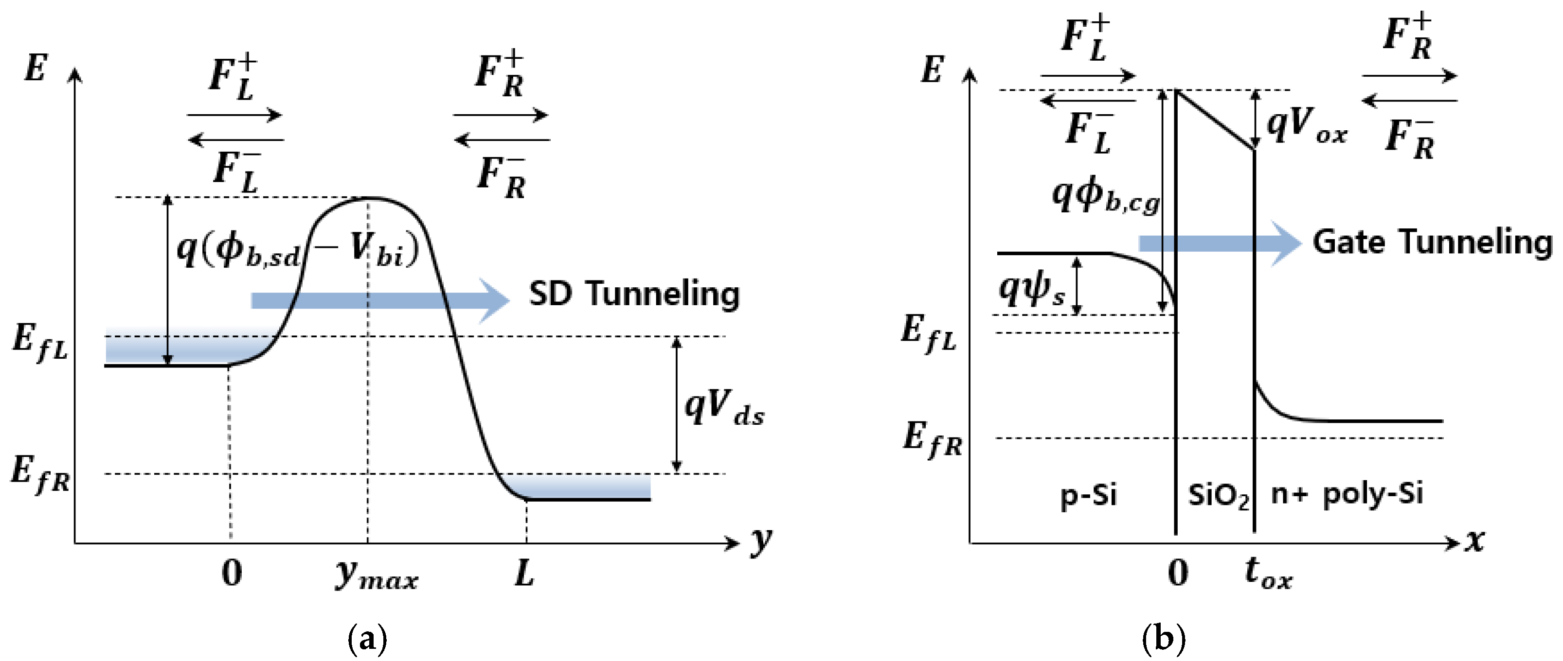
where is the charge; is the Planck’s constant; is the effective mass, and and 3 correspond to source-drain and the channel-gate tunneling, respectively. and are the Fermi–Dirac distribution functions of the transversal energy and longitudinal energy at the left and right reservoirs, respectively. For 1D DOS based on carbon nanotubes and Si nanowires, the tunneling current can be expressed as an integral over the longitudinal energy [7,24,25]. By an extension of the formulation of (1), the model for p-channel Ge nanowire is modified to take into account phonon and surface roughness scattering in the channel and SD tunneling [25,26]. is the tunneling probability of the energy barrier between source and drain or between channel and gate . The tunneling probability is given by the WKB integral for the energy barrier profile as
where, is the reduced Planck’s constant; and are the turning points at which is equal to ; and is in x-direction for the channel-gate tunneling and in y-direction for source-drain tunneling, respectively, as shown in Figure 1. Using the WKB approximation of (2) for parabolic and trapezoidal barriers of the SD and gate tunneling, respectively, compact models for the tunneling probability can be obtained to derive analytical formulations of the tunneling current and its shot noise [4,7,16,19]. For the source-drain tunneling path, when the channel length is sufficiently short, the barrier potential can be approximately represented by a parabolic function of y as [5,7]
where has a local maximum at . The boundary conditions are and , which yield
where is the built-in potential of the source-channel junction, and is the drain-source voltage. The maximum barrier height is expressed as a function of and
where is the surface potential calculated by an explicit model [27], and is the threshold voltage shift due to drain-induced barrier lowering (DIBL) [4]. By substituting (3) into (2) and performing the integral in (2), the source-drain tunneling probability is obtained as
where is the electron effective mass along the y-direction.
The gate tunneling mechanisms can be primarily divided into Fowler–Nordheim (FN), Poole–Frenkel (PF), and direct tunneling [17,19,23]. For non-stressed devices with a gate oxide thickness below 3 nm, direct tunneling is a dominant mechanism of the gate leakage current [23]. This direct tunneling consists of current components such as channel-gate, S/D-gate, and substrate-gate current. However, for the channel-gate tunneling current becomes a main component, since a higher oxide voltage between the channel and the gate causes the current to be proportional to the channel length [17,23]. For the channel-gate tunneling path through the oxide layer, the barrier potential will be , where is the barrier height above the conduction band edge at the Si-SiO2 interface; is the oxide voltage, and is the oxide thickness. Integration of (2) from to for the gate tunneling probability with gives [16,17]
where is the electron effective mass in the oxide.
Introducing the ballistic efficiency associated with the carrier flows and integrating over in (1), the general form of the tunneling currents is given by
where is the Boltzmann constant; is the temperature; and are the Fermi-energy level from the ground energy at the left and right reservoirs, respectively, and is the Fermi–Dirac integral. For the source-drain current, (9) gives the total current incorporating both the tunneling current in the subthreshold region and the thermionic current in the inversion region [1,2,3,4,5].
3. Shot Noise Model
Shot noise is expressed by introducing the Fano factor defined as , being the spectral density of current fluctuations at low frequency (). Full shot noise () is expected if the electrons tunneling through the barrier follow Poisson statistics. The Fano factor is suppressed () or enhanced (), depending on correlations associated with the carrier behavior. The microscopic mechanisms responsible for shot noise have been associated with sequential or coherent tunneling through the potential barrier [28,29]. In the sequential tunneling (ST) model, the interaction of carriers results in other tunneling events due to fluctuations in the potential [16,21,28,29]. In the case of stress-induced leakage currents (SILCs) through the gate oxide, the noise properties are explained by trap-assisted tunneling, a two-step process in which electrons first tunnel from the channel to a trap in the oxide, then from the trap to the gate [12,21,22,23,24,25,26,27,28,29,30]. Analogously, by introducing a two-step tunneling process for the single barrier in both the source-drain and channel-gate direction, we can define four different flow rates, namely, the generation flow rate injected from the left or right ( or ) and the recombination flow rate transmitted to the left or right ( or ), as shown in Figure 1a,b [31,32,33]. The electron transport is governed by the total number of carriers between the left reservoir and the barrier, . In the presence of a generation-recombination process, the flow rates are modulated by the statistical fluctuation of the state occupancies of the left and right reservoir, leading to a number fluctuation [21]. Using the Langevin equation for the number fluctuation and performing a Fourier transform, the Fano factor is obtained as [16,21,28,29]
where is the average of ; and and are the characteristic times related to due to current fluctuations through the left and right reservoirs, respectively. If the flow rate of injected carriers from the left, , in the single barrier is independent of , then the characteristic times and given in (12) are represented by the derivatives of the carrier flow to the left, , and to the right, , respectively. By extending the Landauer Formula (1), and take the forms
In order to calculate the flow rate of carriers for 1D DOS, (13) and (14) can be replaced by integration over the longitudinal energy [11,24]. Taking the derivatives of (13) and (14) with respect to leads to the expression ( = 1 for L and = 2 for R)
For source-drain tunneling, the source-drain voltage is approximately independent of , and therefore. By differentiating (7) with respect to and combining all electrostatic effects in a geometrical gate capacitance , the derivatives of the first term in (16) become
where ; is the oxide capacitance; , , and are the quantum capacitances of the gate, source, and drain, respectively, and is the 2D DOS in the channel [10,30]. In the case of channel-gate tunneling through the oxide layer, the derivatives are obtained from (8) and (16) as
where , , , and [16]. Note that the set of (11), (12), and (15)–(20) provide the analytical formulation of the shot noise as a function of the applied voltages.
In the coherent tunneling (CT) model, there is no electron scattering during electron transmission through the barrier and the transport is governed by the total transparency of the barrier [14,29]. In the zero frequency limit, the shot noise is given by
where the first and second term describe the injection noise and the partition noise of coherent tunneling, respectively.
4. Results and Discussion
For the calculation of the current and noise, the Fermi-energy of the gate must be numerically solved using the relation [34]
where is the thermal voltage, and is the threshold voltage. The Fermi energy of the source for the entire on-state and subthreshold behavior is given by [34]
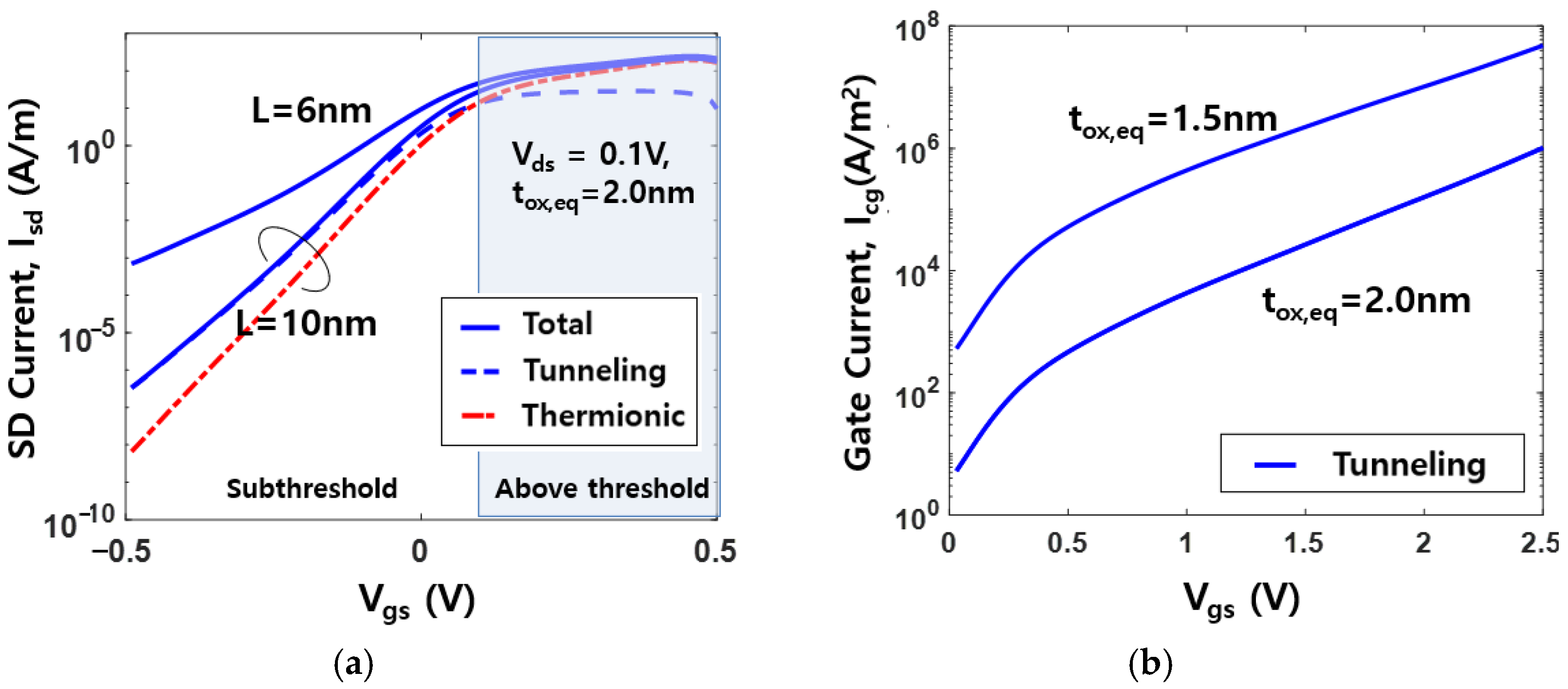
with and . Figure 2a,b show the calculated SD and gate current, respectively, as functions of for different channel lengths and oxide thicknesses.
The simulation for an n+ poly-Si nMOSFET with nitrided oxide was performed using (9) and (10) with =2.6 eV =1.5/2.0 nm, ,, , , for , and for . In the case of high- dielectric/metal gate stack, the equivalent oxide thickness should be carefully estimated by the capacitance measurement, because a replacement of gate stack alters the electrical thickness of oxide [35]. For the SD current in the subthreshold region, the tunneling contribution becomes dominant, and thermionic contribution is reduced owing to the high channel barrier.
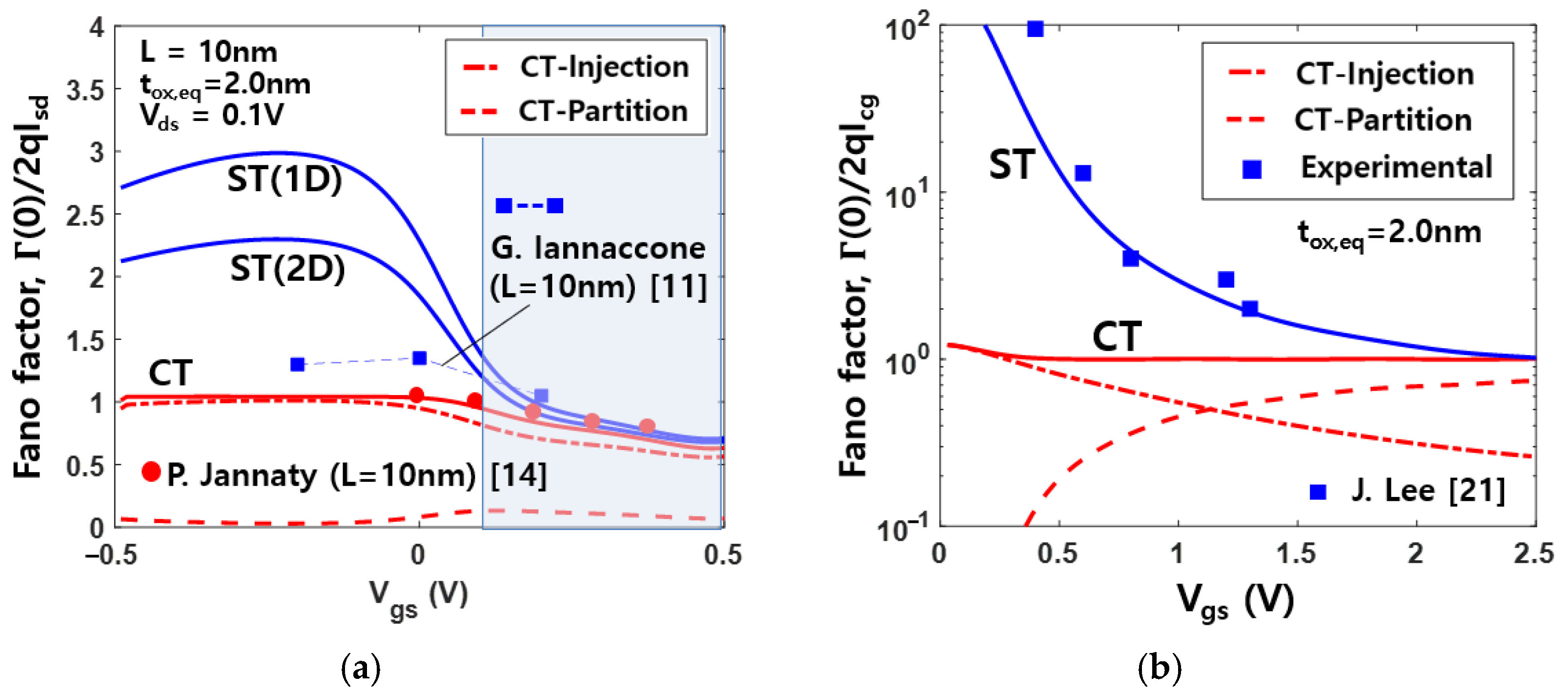
Figure 3a,b show the comparisons between ST and CT model of the Fano factor for SD and gate tunneling shot noise, respectively, as functions of . As can be seen from Figure 3a, in the subthreshold region, the noise in the SD current is enhanced , owing to the positive correlation between tunneling into the channel caused by the interplay between the DOS and electrostatics [11,14]. This is consistent with the results obtained by statistical Monte Carlo simulations [11,36], quantum-mechanical injection model [37,38], and Fermi statistics [39]. Actually, the noise enhancement in the subthreshold region is due to the fact that at low source-drain voltage (), the current is small, while the spectral density of shot noise tends to a finite value, because of the thermal noise contribution [14].
The results in Figure 3a point out the difference for 2D and 1D DOS when the sequential model is used. The Fano factor for 1D DOS is calculated by using the modified formulations of the SD current of (1), the flow rate of carriers of (13) and (14), and the quantum capacitances of (18). When the dimensionality of DOS is reduced, only few electrons take part in transport so that SD current fluctuations normalized to the SD current can heavily affect the noise behavior [40,41]. For moderately high voltages in the inversion region, is so low that injection noise from the left reservoir is dominant, leading to noise suppression () [14,40,41].
As shown in Figure 3b, for verification of the shot noise model for the gate tunneling current, the simulation results are compared with the measured Fano factor for an n+ poly-Si nMOSFET as a function of [21]. It can be seen that large enhancement in gate shot noise at low voltages is in good agreement with the experimental results. This is due to the fact that both of the inverse time constants of the ST model are nearly equal in magnitude, but of opposite signs [16,28,42,43]. As increases, the tunneling probability becomes higher, and noise following a partition process appears [14,44].
5. Conclusions
The general expressions of current and noise are found to be well-suited for computation in a unified manner of the Fano factor of both SD and gate shot noise in sub-10 nm MOSFETs. The sequential tunneling model associated with the number fluctuations predicts enhancement of the shot noise in the SD tunneling current in the subthreshold regime, thus extending the validity of the model to the enhancement of shot noise in the gate tunneling current at low voltages. The resulting analytical compact models may be considered suitable in circuit simulators for circuit-level simulation.
Funding
This work was supported by the National Research Foundation of Korea (NRF) grant funded by the Korea government (MSIT) (No. 2019R1F1A1050640).
Data Availability Statement
The data presented in this study are available on request from the corresponding author.
Conflicts of Interest
The author declares no conflict of interest.
References
- Markov, S.; Kwok, Y.; Li, J.; Zhou, W.; Zhou, Y.; Chen, G. Fundamental limit to scaling Si field-effect transistors due to source-to-drain direct tunneling. IEEE Trans. Electron Devices 2019, 66, 1167–1173. [Google Scholar] [CrossRef]
- Natori, K. Ballistic metal-oxide-semiconductor field effect transistor. J. Appl. Phys. 1994, 76, 4879–4890. [Google Scholar] [CrossRef] [Green Version]
- Naveh, Y.; Likharev, K.K. Modeling of 10nm-scale ballistic MOSFET’s. IEEE Electron Device Lett. 2000, 21, 242–244. [Google Scholar] [CrossRef]
- Lin, Y.K.; Duarte, J.P.; Kushwaha, P.; Agarwal, H.; Chang, H.L.; Sachid, A.; Salahuddin, S.; Hu, C. Compact modeling source-to-drain tunneling in sub-10nm GAA FinFET with industry standard model. IEEE Trans. Electron Devices 2017, 64, 3576–3581. [Google Scholar] [CrossRef]
- Hiblot, G.; Rafhay, Q.; Boeuf, F.; Ghibaudo, G. Analytical relationship between subthreshold swing of thermionic and tunneling currents. Electron. Lett. 2014, 50, 1745–1747. [Google Scholar] [CrossRef]
- Kawaura, H.; Baba, T. Direct tunneling from source to drain in nanometer-scale silicon transistor. Jpn. J. Appl. Phys. 2003, 42, 351–357. [Google Scholar] [CrossRef]
- Cheng, H.; Liu, T.; Zhang, C.; Yang, Z.; Liu, Z.; Nakazato, K.; Zhang, Z. Nanowire gate-all-around MOSFETs modeling: Ballistic transport incorporating the source-to-drain tunneling. Jpn. J. Appl. Phys. 2020, 59, 1–9. [Google Scholar] [CrossRef]
- Seoane, N.; Martinez, A. A detailed coupled-mode-space non-equilibrium Green’s function simulation study of source-to-drain tunneling in gate-all-around Si nanowire metal oxide semiconductor field effect transistors. J. Appl. Phys. 2013, 114, 104307. [Google Scholar] [CrossRef]
- Naveh, Y.; Korotkov, A.N.; Likharev, K.K. Shot noise suppression in multimode ballistic Fermi conductors. Phys. Rev. B. 1998, 60, R2169–R2172. [Google Scholar] [CrossRef] [Green Version]
- Mugnaini, G.; Iannaccone, G. Channel noise modeling of nanoMOSFETs in a partially ballistic transport regime. J. Comput. Electron. 2006, 5, 91–95. [Google Scholar] [CrossRef]
- Iannaccone, G.; Betti, A.; Fiori, G. Suppressed and enhanced shot noise in one dimensional field-effect transistors. J. Comput. Electron. 2015, 14, 94–106. [Google Scholar] [CrossRef]
- Iannaccone, G. Analytical and numerical investigation of noise in nanoscale ballistic field effect transistors. J. Comput. Electron. 2004, 3, 199–202. [Google Scholar] [CrossRef] [Green Version]
- Jia, X.; He, L. Research of shot noise based on realistic nano-MOSFETs. AIP Adv. 2017, 7, 055202. [Google Scholar] [CrossRef] [Green Version]
- Jannaty, P.; Sabou, F.C.; Le, S.T.; Donato, M.; Bahar, R.I.; Patterson, W.; Mundy, J.; Zaslavsky, A. Shot-noise-induced failure in nanoscale flip-flops-Part I: Numerical framework. IEEE Trans. Electron Devices 2012, 59, 800–806. [Google Scholar] [CrossRef]
- Spathis, C.; Birbas, A.; Georgakopoulou, K. Semi-classical noise investigation for sub-40 nm metal-oxide-semiconductor field-effect transistors. AIP Adv. 2015, 5, 087114. [Google Scholar] [CrossRef]
- Lee, J.; Bosman, G.; Green, K.R.; Ladwig, D. Model and analysis of gate leakage current in ultrathin nitrided oxide MOSFETs. IEEE Trans. Electron Devices 2002, 49, 1232–1241. [Google Scholar]
- Ranuarez, J.C.; Deen, M.J.; Chen, C.H. A review of gate tunneling current in MOS devices. Microelectron. Rel. 2006, 46, 1939–1956. [Google Scholar] [CrossRef]
- Clerc, R.; O’Sullivan, P.; McCarthy, K.G.; Ghibaudo, G.; Pananakakis, G.; Mathewson, A. A physical compact model for direct tunneling from NMOS inversion layers. Solid-State Electron. 2001, 45, 1705–1716. [Google Scholar] [CrossRef]
- Gehring, A.; Selberherr, S. Modeling of tunneling current and gate dielectric reliability for nonvolatile memory devices. IEEE Trans. Device Mater. Rel. 2004, 4, 306–319. [Google Scholar] [CrossRef]
- Mao, L.F.; Li, X.J.; Wang, Z.O.; Wang, J.Y. The gate leakage current in graphene field-effect transistor. IEEE Electron Device Lett. 2008, 29, 1047–1049. [Google Scholar] [CrossRef]
- Lee, J.; Bosman, G.; Green, K.R.; Ladwig, D. Noise model of gate-leakage current in ultrathin oxide MOSFETs. IEEE Trans. Electron Devices 2003, 50, 2499–2506. [Google Scholar]
- Deen, M.J.; Chen, C.H.; Asgaran, S.; Rezvani, G.A.; Tao, J.; Kiyota, Y. High-frequency noise of modern MOSFETs: Compact modeling and measurement issues. IEEE Trans. Electron Devices 2006, 53, 2062–2081. [Google Scholar] [CrossRef]
- Manghisoni, M. Gate current noise in ultrathin oxide MOSFETs and its impact on the performance of analog front-end circuits. IEEE Trans. Nucl. Sci. 2008, 55, 2399–2407. [Google Scholar] [CrossRef]
- Taur, Y.; Wu, J.; Min, J. Dimensionality dependence of TFET performance down to 0.1 V supply voltage. IEEE Trans. Electron Devices 2016, 63, 877–880. [Google Scholar] [CrossRef]
- Chun, M.W.; Wong, K.L.; Hamzah, A.; Rusli, S.; Alias, N.E.; Lim, C.S.; Tan, M.L.P. A review of the top of the barrier nanotransistor models for semiconductor nanomaterials. Superlatt. Microstruct. 2020, 140, 106429. [Google Scholar] [CrossRef]
- Tanaka, H.; Suda, J.; Kimoto, T. Analysis of ballistic and quasi-ballistic hole properties in germanium nanowires based on an extended “Top of the Barrier” model. Solid-State Electron. 2016, 123, 143–149. [Google Scholar] [CrossRef]
- Pregaldiny, F.; Lallement, C.; van Langevelde, R.; Mathiot, D. An advanced explicit surface potential model physically accounting for the quantization effects in deep-submicron MOSFETs. Solid-State Electron. 2004, 48, 427–435. [Google Scholar] [CrossRef]
- Aleshkin, V.Y.; Reggiani, L. Electron transport and shot noise in double-barrier resonant diodes: The role of Pauli and Coulomb correlations. Phys. Rev. B. 2001, 64, 245333. [Google Scholar] [CrossRef]
- Aleshkin, V.Y.; Reggiani, L. Comparative analysis of sequential and coherent tunneling in resonant diodes. Phys. Rev. B. 2006, 73, 165320. [Google Scholar] [CrossRef]
- Iannaccone, G.; Crupi, F.; Neri, B.; Lombardo, S. Theory and experiment of suppressed shot noise in stress-induced leakage current. IEEE Trans. Electron Devices 2003, 50, 1363–1369. [Google Scholar] [CrossRef]
- Datta, S.; Assad, F.; Lundstrom, M.S. The Si MOSFET from a transmission viewpoint. Superlatt. Microstruct. 1998, 23, 771–780. [Google Scholar] [CrossRef]
- Rahman, A.; Lundstrom, M.S. A compact scattering model for the nanoscale double-gate MOSFET. IEEE Trans. Electron Devices 2002, 49, 481–489. [Google Scholar] [CrossRef]
- Natori, K. Comapct modeling of ballistic nanowire MOSFETs. IEEE Trans. Electron Devices 2008, 55, 2877–2885. [Google Scholar] [CrossRef] [Green Version]
- Marin, E.G.; Bader, S.J.; Jena, D. A new holistic model of 2-D semiconductor FETs. IEEE Trans. Electron Devices 2018, 65, 1239–1245. [Google Scholar] [CrossRef]
- Robertson, J.; Wallace, R.M. High-k materials and metal gates for CMOS applications. Materi. Sci. Eng. R. 2015, 88, 1–41. [Google Scholar] [CrossRef] [Green Version]
- Betti, A.; Fiori, G.; Iannaccone, G. Enhanced shot noise in carbon nanotube field-effect transistors. Appl. Phys. Lett. 2009, 95, 252108. [Google Scholar] [CrossRef] [Green Version]
- Oriols, X. Quantum mechanical effects on noise properties of nanoelectronic devices: Application to Monte Carlo simulation. IEEE Trans. Electron Devices 2003, 50, 1830–1836. [Google Scholar] [CrossRef]
- Oriols, X.; Martin, F.; Sune, J. Approach to study the noise properties in nanoscale electronic devices. Appl. Phys. Lett. 2001, 79, 1703–1705. [Google Scholar] [CrossRef] [Green Version]
- Gonzalez, T.; Mateos, J.; Pardo, D.; Gomila, G.; Cantalapiedra, I.R.; Reggiani, L. Role of energy correlations on Coulomb suppression of shot noise in ballistic conductors contacted to degenerate reservoirs. Phys. Rev. B. 2003, 68, 075309. [Google Scholar] [CrossRef] [Green Version]
- Betti, A.; Fiori, G.; Iannaccone, G. Shot noise suppression in quasi-one-dimensional field-effect transistors. IEEE Trans. Electron Devices 2009, 56, 2137–2143. [Google Scholar] [CrossRef] [Green Version]
- Oriols, X.; Fernandez-Diaz, E.; Alvarez, A.; Alarcon, A. An electron injection model for time-dependent simulators of nanoscale devices with electron confinement: Application to the comparison of the intrinsic noise of 3D-, 2D-, 1D-ballistic transistors. Solid-State Electron. 2007, 51, 306–319. [Google Scholar] [CrossRef]
- Aleshkin, V.Y.; Reggiani, L.; Reklaitis, A. Current instability and shot noise in nanometric semiconductor heterostructures. Nanotechnology 2000, 73, 370–374. [Google Scholar] [CrossRef]
- Aleshkin, V.Y.; Reggiani, L. Reklaitis, Sub- and super-Poissonian shot noise in single-barrier semiconductor structures. Semicond. Sci. Technol. 2000, 15, 1045–1048. [Google Scholar] [CrossRef]
- Bulashenko, O.M.; Rubi, J.M. Quantum suppression of shot noise in field emitters. Phys. Rev. B. 2003, 67, 115222. [Google Scholar] [CrossRef] [Green Version]
Figure 1.
Representation of energy barrier profile (a) along the y-axis in the source-drain direction and (b) along the x-axis in the channel-gate direction.
Figure 1.
Representation of energy barrier profile (a) along the y-axis in the source-drain direction and (b) along the x-axis in the channel-gate direction.

Figure 2.
(a) Calculated SD current versus
for (b) calculated gate tunneling current versus for different .
Figure 2.
(a) Calculated SD current versus
for (b) calculated gate tunneling current versus for different .

Figure 3.
Comparison between ST model and CT model of Fano factor as a function of
for (a) SD current noise and (b) gate tunneling current noise.
Figure 3.
Comparison between ST model and CT model of Fano factor as a function of
for (a) SD current noise and (b) gate tunneling current noise.

Publisher’s Note: MDPI stays neutral with regard to jurisdictional claims in published maps and institutional affiliations. |
© 2021 by the author. Licensee MDPI, Basel, Switzerland. This article is an open access article distributed under the terms and conditions of the Creative Commons Attribution (CC BY) license (https://creativecommons.org/licenses/by/4.0/).
Share and Cite
MDPI and ACS Style
Lee, J. Unified Model of Shot Noise in the Tunneling Current in Sub-10 nm MOSFETs. Nanomaterials 2021, 11, 2759. https://0-doi-org.brum.beds.ac.uk/10.3390/nano11102759
AMA Style
Lee J. Unified Model of Shot Noise in the Tunneling Current in Sub-10 nm MOSFETs. Nanomaterials. 2021; 11(10):2759. https://0-doi-org.brum.beds.ac.uk/10.3390/nano11102759
Chicago/Turabian StyleLee, Jonghwan. 2021. "Unified Model of Shot Noise in the Tunneling Current in Sub-10 nm MOSFETs" Nanomaterials 11, no. 10: 2759. https://0-doi-org.brum.beds.ac.uk/10.3390/nano11102759
Note that from the first issue of 2016, this journal uses article numbers instead of page numbers. See further details here.