Article

Correlation between Optical Localization-State and Electrical Deep-Level State in In0.52Al0.48As/In0.53Ga0.47As Quantum Well Structure

1
Quantum-Functional Semiconductor Research Center, Dongguk University-Seoul, Seoul 04620, Korea
2
Division of Physics & Semiconductor Science, Dongguk University-Seoul, Seoul 04620, Korea
*
Author to whom correspondence should be addressed.
Submission received: 13 February 2021 / Revised: 23 February 2021 / Accepted: 25 February 2021 / Published: 26 February 2021

Abstract

:
The peculiar correlationship between the optical localization-state and the electrical deep-level defect-state was observed in the In0.52Al0.48As/In0.53Ga0.47As quantum well structure that comprises two quantum-confined electron-states and two hole-subbands. The sample clearly exhibited the Fermi edge singularity (FES) peak in its photoluminescence spectrum at 10–300 K; and the FES peak was analyzed in terms of the phenomenological line shape model with key physical parameters such as the Fermi energy, the hole localization energy, and the band-to-band transition amplitude. Through the comprehensive studies on both the theoretical calculation and the experimental evaluation of the energy band profile, we found out that the localized state, which is separated above by ~0.07 eV from the first excited hole-subband, corresponds to the deep-level state, residing at the position of ~0.75 eV far below the conduction band (i.e., near the valence band edge).

1. Introduction

InAlAs/InGaAs heterostructures have been widely studied in various aspects because of their vast potentials in both ultrahigh-speed electronic devices and highly-efficient optoelectronic devices that can operate in the infrared regimes. For instance, the high electron-mobility transistors [1,2,3,4] and the spin field-effect transistors [5] are feasible electronic devices that could be demonstrated on InAlAs/InGaAs heterostructures. In addition, the infrared photodetectors [6,7,8,9], X-ray detectors [10], terahertz (THz) quantum-cascade lasers [11,12], mid-infrared quantum-cascade lasers [13,14], and electro-optical modulators [15] are also typical examples that can open up a broad avenue toward the tangible optoelectronic applications of the InAlAs/InGaAs quantum well (QW) structures. When growing the epitaxial heterostructure, in general, both the alloy disorder and the layer-thickness fluctuation are inevitable because of the lattice mismatch in between the ultrathin heterojunction layers. This would eventually create interfacial defects, forming both the electrical deep-level states and the optical localization states inside the heterojunction. According to previous literature, those energy states may cause the Fermi-edge singularity (FES) phenomena [16,17,18,19,20,21], leading to the abnormal luminescence [21,22,23] and the anomalous carrier transport behaviors [24]. Furthermore, such an FES is known to significantly affect the device performances (e.g., decreased carrier mobility [25,26], increased kink-effect in resonant tunneling [27], cotunneling during the single-electron transport [28], increased electron-phonon coupling [29], increased electron-electron scattering in the photodiode [30], etc.). Based upon the above, one can conjecture that the FES-related states should be simultaneously represented with both the electronic band structures and the energy band diagram, respectively. To clarify this, thus, a comprehensive study on the relationship between the FES-related optical localization state and the electrical deep-level state is required to elucidate the essence of the correlation. However, the FES behaviors in the InAlAs/InGaAs QW systems still remain as a vivid debate.
Aiming at investigating how the FES behaviors correlate with the optical and the electronic energy band structures in the InGaAs/InAlAs QW, we thoroughly examined its FES-related localized-energy states by systematic analyses of temperature-dependent photoluminescence (PL) spectroscopy and Fourier-transform deep-level transient spectroscopy (FT-DLTS). Key procedures of this research can be described as follows: (1) calculation of the electronic band structure by using the self-consistent Schrödinger-Poisson equation [31,32], (2) observation of two abnormal PL features (i.e., appearance of the temperature-independent FES peak; and observation of all the red-shifted inter-subband transitions, comparing with the calculated band profile), (3) deconvolution of the low-temperature PL spectrum by using the phenomenological line-shape model [33], (4) extraction of the FES-related localization state; and verification of its corresponding red-shift in PL spectra, and (5) corroboration of the optical localization state by observing the electrical deep-level state through FT-DLTS. Herein, we describe and discuss the aforementioned theoretical and experimental results in detail.

2. Sample and Experimental Scheme

Figure 1a schematically illustrates the In0.53Ga0.47As/In0.52Al0.48As QW structure that has been grown onto the (100) InP substrate by molecular beam epitaxy (MBE). Firstly, the InP surface was pre-cleaned by thermal heating at 520 °C in the MBE chamber. Then, the 500-nm-thick In0.52Al0.48As buffer layer was grown onto the (100) InP surface at 475 °C. Subsequently, the undoped In0.53Ga0.47As layer (12 nm) and the undoped In0.52Al0.48As spacer (4 nm) were grown onto the buffer layer at the same temperature.
Next, the Si delta-doped sheet (4.5 × 1012 cm−2) and the undoped In0.52Al0.48As barrier layer (20 nm) were sequentially grown on the spacer layer. Finally, the 5-nm-thick cap layer of n-doped In0.53Ga0.47As was deposited on top of the sample in order to assist the Ohmic contact formation during the device fabrication steps [34].
To examine the optical properties of the sample, the temperature-dependent PL measurements were carried out at 10–300 K by using a home-built PL system [35,36], where the picosecond diode laser (λlaser = 634 nm) and the time-correlated single-photon counter were equipped as an excitation source and a light emission detector, respectively. The excitation power density was fixed at 50 W/cm2 for all measurements. In order to extract the subband structure in the InGaAs/InAlAs QW, the PL spectra were analyzed by line-shape fitting in terms of the localization energy theorem [33]. In addition, the FT-DLTS measurements were also carried out to compare the energy values between the optical localization state with the electrical deep-level state. For the DLTS measurements, the Schottky contact was formed onto the top surface of the sample. Namely, after recess-etching of the n-In0.53Ga0.47As cap layer, the circular Ti/Au Schottky electrode (ϕdia ~ 300 μm) was formed onto the In0.52Al0.48As barrier layer. The Ohmic contact was formed onto the unrecessed n-InGaAs cap layer in the form of the ring electrode at the vicinity of the circular Schottky contact. After fabricating the Schottky diode structure, the DLTS measurements were performed with a 100 mV ac test signal at 1 MHz using a Bio-Rad DL8000 DLTS system (PhysTech, Moosburg, Germany).

3. Results and Discussion

3.1. Calculation of Energy Band Profile

Prior to the experimental characterization, we calculated the energy band diagram of the In0.53Ga0.47As/In0.52Al0.48As QW system to understand the quantum mechanical electric-energy structure of the fabricated sample. Figure 1b displays the energy band profile of the MBE-grown In0.53Ga0.47As/In0.52Al0.48As QW structure, which was calculated by using a Nextnano3 simulator (Nextnano GmbH, München, Germany) that had been programmed in terms of the transfer matrix function based on the self-consistent Schrödinger-Poisson equations [31,32]. From the calculated energy band profile, one may expect that several types of optical transitions are theoretically available because two excited electron-subbands (i.e., E1 and E2) and two excited hole-states (i.e., H1 and H2) coexist in the In0.53Ga0.47As/In0.52Al0.48As QW. In addition, the radiative optical transition between the Fermi level (EF) and H1 is also possible because of strong carrier population by δ-doping. The key transition parameters are listed in Table 1, where ΔEiHj (= EiHj) denotes the energy gap between the quantum mechanical subbands.

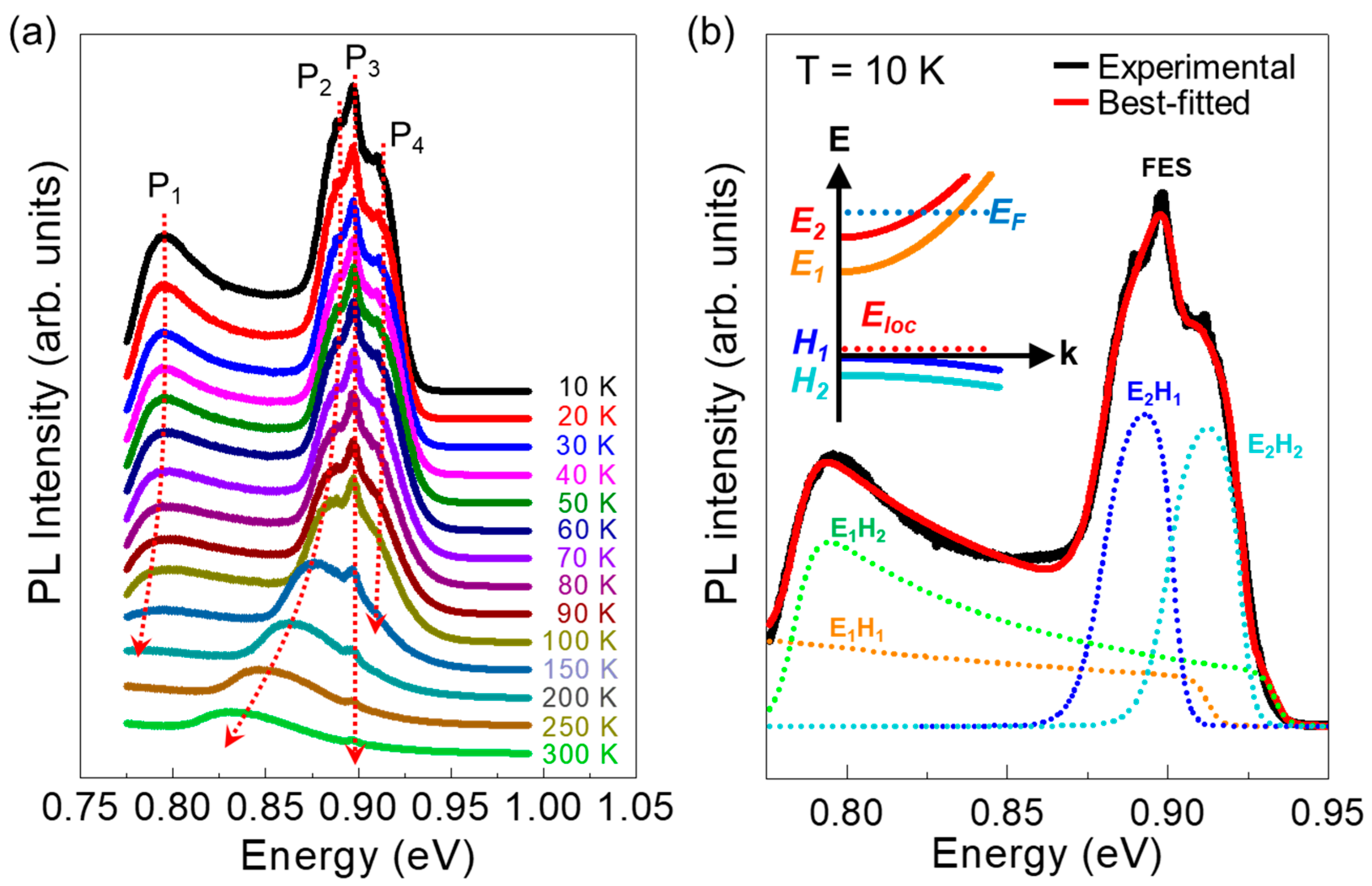
3.2. Temperature Dependent PL Characteristics

After elucidating the energy band profile and the theoretically available optical transitions, we characterized the experimental emission properties of the MBE-grown InGaAs/InAlAs QW. Figure 2a shows the temperature-dependent PL spectra at 10–300 K of the sample. At 10 K, the InGaAs/InAlAs QW clearly exhibits four predominant PL peaks at P1, P2, P3, and P4, which correspond to E1H2, E2H1, FES, and E2H1 transitions, respectively, as discussed later. Here, it should be noticed that two abnormal PL features occur in the present InGaAs/InAlAs QW system. One is the temperature-independent behavior of the P3 peak; and the other is the approximately 70 meV red-shift of all the peaks, compared to the theoretically-available optical-transition energy values. We attribute the former to the FES phenomena because such an unusual temperature-independent PL feature could be explained by the many-body effect of the FES, arising from the Coulomb interaction between the photogenerated electron-hole pairs and the electrons in the Fermi sea [16,34]. The latter of the anomalously red-shifted inter-subband transition energies could also be ascribed to the FES nature because the FES causes a red-shift of the inter-subband emission due to the strongly-localized energy-state at the valence band edge of the InGaAs/InAlAs QW, as discussed below in Section 3.3.

3.3. Extraction of Inter-Subband Transition Energy Values via PL Line Shape Fitting

To clarify the above hypothesis, we carried out the line shape analysis of the low-temperature PL spectrum by using a localization energy state-included phenomenological fitting model [33]. According to this model, the total PL intensity can be represented as
I ( ω ) = A i j D ( ω ) f e i ( ω ) f h j ( ω )
where Aij is the transition coefficient including the inter-subband matrix elements; D is the broadened density-of-states step function; fei and fhj are the Fermi distribution functions for electron and heavy-hole subbands, respectively. As shown in the deconvoluted PL spectra obtained from the above model (Figure 2b), the original PL spectrum could be well-resolved by four peaks. We could assign these four peaks as inter-subband transitions (EiHj); i.e., E1H1, E1H2 (= P1), E2H1 (= P2), and E2H2 (= P4), because of the following reasons. First of all, we here note that E1H1 was not labelled in Figure 2a because its exact peak had not emerged in the spectral range. Due to its explicit nature from the quantum mechanical calculation, however, the E1H1 peak should be included in the line shape fitting model. As summarized in the rightmost column in Table 1, consequently, the transition energies of E1H1, E1H2, E2H1, and E2H2 are red-shifted by ~70 meV from the theoretical values. Through integrating those four original EiHj transitions (i.e., dashed curves), additionally, the localization state-associated sharp FES (= P3) peak has clearly appeared in the best-fitted curve (i.e., red line). Furthermore, the three main peaks of E2H1, E2H2, and FES (i.e., stronger peaks) have an identical red-shift value of 70 meV. Accordingly, one can deduce that the inter-subband transition energies might be decreased parallelly by a single origin such as a localization energy state (Eloc).

3.4. Extraction of Optical Localization State

Based upon the above concept, we can therefore draw the schematic band structure at the k-space (Figure 2b, inset). Considering the existence of Eloc, we here assumed that the H1 state is the base level; and two heavy H1 and H2 bands contain the hole occupation probability. Then, the extracted parameters could be taken into account via the many-body effects, so-called FES phenomena [16,34]. The above assumption can be verified by three following results: (1) the magnitude of ΔE1E2 (i.e., E1E2 = 120 meV) equals to each other in between theoretical and experimental cases; (2) the total carrier density (n ≈ 3.49 × 1012 cm−2) coincides with that obtained in our previous mobility spectrum analysis (n ≈ 3.43 × 1012 cm−2 [34]). Here, the total carrier density was estimated using the observed ”EFEj” value by the following formula:
n j 2 D = m j 2 π k B T l n [ 1 + e x p ( E F E j k B T ) ]
where m j is the effective mass; kB is the Boltzmann constant; j is 1 or 2 for the two subbands; T is the temperature; is the reduced Planck constant; EF is the Fermi energy, and Ej is the jth subband energy; (3) when comparing all the parameters, ΔEFEloc (= EFEloc = EFES = 0.90 eV) is experimentally available, which signifies the localized state to locate at the valence band edge of the QW; then (4) ΔElocH1 (= ElocH1) should be 70 meV, leading to the red-shift of the PL peaks by 70 meV because most of the excited carriers would transit into the localized state. As a result, the FES phenomena can take place between the localized state and the Fermi level.

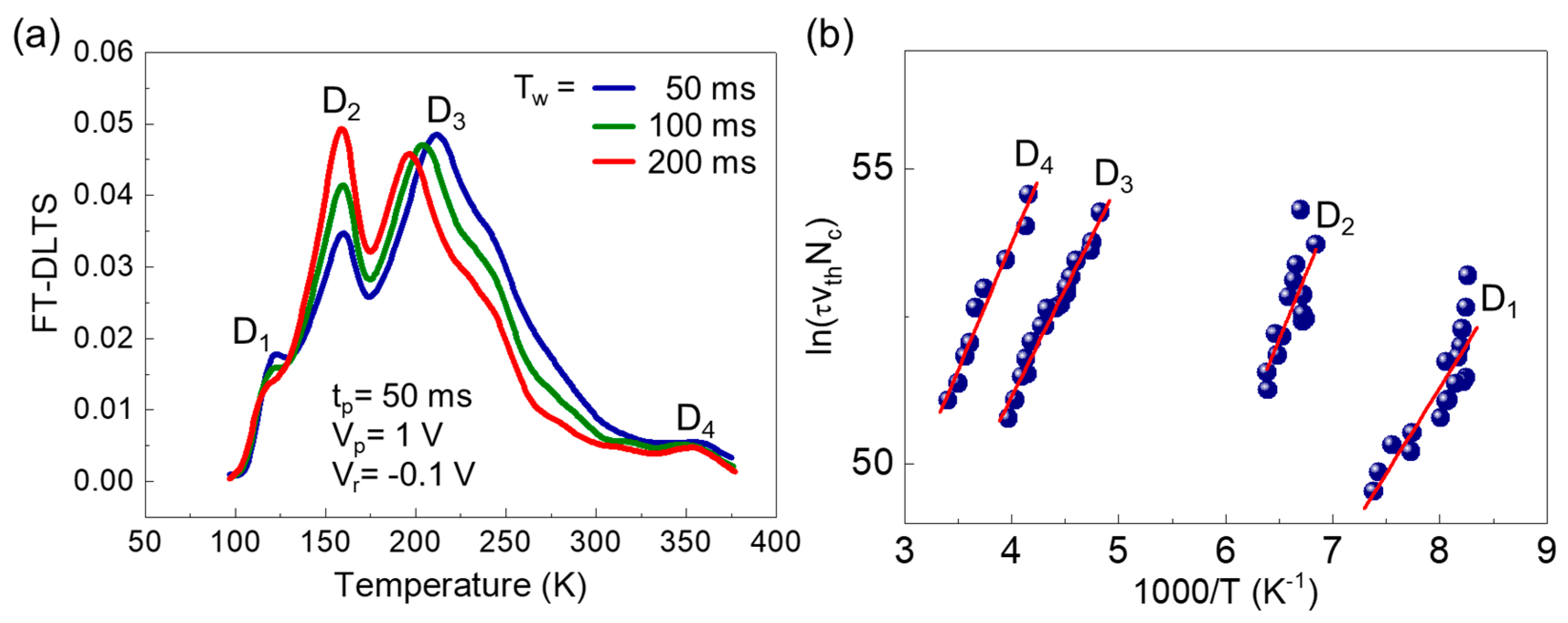
3.5. Corroboration of Energetic Position for Localized State by DLTS

The energetic position of the localized state can be further corroborated by observing its corresponding electrical deep-level state. For more clarity on the localized state position, we carried out FT-DLTS measurements [37]. Figure 3a shows the isothermal period (Tw)-dependent FT-DLTS signals measured under the reverse bias voltage (Vr = −0.1 V) applied to the Schottky electrode, the filling pulse voltage (Vp = 1 V), the filling pulse time (tp = 50 ms). The sample exhibits four DLTS signals of D1, D2, D3, and D4. Among them, one should focus on the peculiar phenomenon that, when varying Tw from 50 to 200 ms, the position of the D2 signal is fixed at ~150 K while its intensity becomes larger. Such an unusual Tw-independent DLTS peak position is indicative of the localized state rather than band-like state [38]. In Figure 3b, the Arrhenius plots of the DLTS signals are shown. In the case of D2, the slope is steeper than the others. As summarized in Table 2, accordingly, the D2 possesses more substantial defect parameters. Particularly, in the present work, we focus on the energetic position of the D2 level (i.e., ECET ≈ 0.75 eV). Considering that In0.53Ga0.47As has a bandgap energy of ~0.75 eV [39,40,41,42], one can expect the localized D2 state to locate its position near the valence band edge. From all the above results, we can conclude that the energetic position of the located D2 state is consistent with that of the optical localization state.

4. Conclusions

We investigated the effects of the localized defect state on both the optical and the electrical properties of the In0.53Ga0.47As/In0.52Al0.48As QW structure. By using the phenomenological PL line shape fitting model, the optical localization energy, Eloc, was determined to be 70 meV. Additionally, through both the optical and the electrical characterizations, the energetic position of the localized state was explicitly confirmed to exist at the valence band edge of the QW. Such a mutual correlation between optical and electrical localization states may lead to the strong confinement of photogenerated carriers. Because of the strong localization, the sample eventually exhibited two abnormal luminescence characteristics (i.e., an appearance of the strong FES persisting up to 300 K and a 70 meV red-shift of all the inter-subband transition energies in parallel).

Author Contributions

Investigation, methodology, formal analysis, and writing—original draft, I.-H.A.; conceptualization and funding acquisition, D.Y.K.; supervision and writing—review and editing, S.L. All authors have read and agreed to the published version of the manuscript.

Funding

This research was supported by National Research Foundation (NRF) of Korea through Basic Science Research Programs (2016R1A6A1A03012877, 2017R1D1A1B03032158, 2019R1A2C1085448) funded by the Korean government.

Institutional Review Board Statement

Not applicable.

Informed Consent Statement

Not applicable.

Conflicts of Interest

The authors declare no conflict of interest.

References

  1. Lee, I.-G.; Jo, H.-B.; Yun, D.-Y.; Shin, C.-S.; Lee, J.-H.; Kim, T.-W.; Ko, D.-H.; Kim, D.-H. Long-channel InAlAs/InGaAs/InAlAs single-quantum-well MISFETs with subthreshold swing of 61 mV/decade and effective mobility of 11900 cm2V−1s−1. Appl. Phys. Express 2019, 12, 64003. [Google Scholar] [CrossRef]
  2. Jo, H.; Baek, J.; Yun, D.; Son, S.; Lee, J.; Kim, T.; Kim, D.; Tsutsumi, T.; Sugiyama, H.; Matsuzaki, H. Lg = 87 nm InAlAs/InGaAs High-Electron- Mobility Transistors with a gm_max of 3 S/mm and fT of 559 GHz. IEEE Electron Device Lett. 2018, 39, 1640–1643. [Google Scholar] [CrossRef]
  3. Yun, D.; Jo, H.; Son, S.; Baek, J.; Lee, J.; Kim, T.; Kim, D.; Tsutsumi, T.; Sugiyama, H.; Matsuzaki, H. Impact of the Source-to-Drain Spacing on the DC and RF Characteristics of InGaAs/InAlAs High-Electron Mobility Transistors. IEEE Electron Device Lett. 2018, 39, 1844–1847. [Google Scholar] [CrossRef]
  4. Ajayan, J.; Nirmal, D. A review of InP/InAlAs/InGaAs based transistors for high frequency applications. Superlattices Microstruct. 2015, 86, 1–19. [Google Scholar] [CrossRef]
  5. Chuang, P.; Ho, S.-C.; Smith, L.W.; Sfigakis, F.; Pepper, M.; Chen, C.-H.; Fan, J.-C.; Griffiths, J.P.; Farrer, I.; Beere, H.E.; et al. All-electric all-semiconductor spin field-effect transistors. Nat. Nanotechnol. 2015, 10, 35–39. [Google Scholar] [CrossRef] [PubMed] [Green Version]
  6. Liu, J.; Lu, J.; Yue, C.; Li, X.; Chen, H.; Wang, L. InAs/InGaAs/InAlAs interband quantum well infrared photodetector (IQWIP) with cut-off response wavelength at 1.93 μm. Appl. Phys. Express 2019, 12, 32005. [Google Scholar] [CrossRef]
  7. Chen, J.; Zhang, Z.; Zhu, M.; Xu, J.; Li, X. Optimization of InGaAs/InAlAs Avalanche Photodiodes. Nanoscale Res. Lett. 2017, 12, 33. [Google Scholar] [CrossRef] [PubMed] [Green Version]
  8. Ma, Y.; Zhang, Y.; Gu, Y.; Chen, X.; Xi, S.; Du, B.; Li, H. Tailoring the performances of low operating voltage InAlAs/InGaAs avalanche photodetectors. Opt. Express 2015, 23, 19278–19287. [Google Scholar] [CrossRef]
  9. Deng, J.; Zong, L.; Bao, W.; Zhu, M.; Liao, F.; Guo, Z.; Xie, Y.; Lu, B.; Wan, J.; Zhu, J.; et al. Integration of MoS2 with InAlAs/InGaAs Heterojunction for Dual Color Detection in Both Visible and Near-Infrared Bands. Adv. Opt. Mater. 2019, 7, 1901039. [Google Scholar] [CrossRef]
  10. Ganbold, T.; Antonelli, M.; Biasiol, G.; Nichetti, C.; Cautero, G.; Menk, R.H. Double-side pixelated X-ray detector based on metamorphic InGaAs/InAlAs quantum well. J. Instrum. 2019, 14, C01014. [Google Scholar] [CrossRef]
  11. Fujita, K.; Yamanishi, M.; Furuta, S.; Tanaka, K.; Edamura, T.; Kubis, T.; Klimeck, G. Indirectly pumped 3.7 THz InGaAs/InAlAs quantum-cascade lasers grown by metal-organic vapor-phase epitaxy. Opt. Express 2012, 20, 20647–20658. [Google Scholar] [CrossRef] [PubMed] [Green Version]
  12. Deutsch, C.; Kainz, M.A.; Krall, M.; Brandstetter, M.; Bachmann, D.; Schönhuber, S.; Detz, H.; Zederbauer, T.; MacFarland, D.; Andrews, A.M.; et al. High-Power Growth-Robust InGaAs/InAlAs Terahertz Quantum Cascade Lasers. ACS Photonics 2017, 4, 957–962. [Google Scholar] [CrossRef] [PubMed]
  13. Mathonnière, S.; Semtsiv, M.P.; Ted Masselink, W. Thermal annealing of lattice-matched InGaAs/InAlAs Quantum-Cascade Lasers. J. Cryst. Growth 2017, 477, 258–261. [Google Scholar] [CrossRef]
  14. Demir, I.; Elagoz, S. Interruption time effects on InGaAs/InAlAs superlattices of quantum cascade laser structures grown by MOCVD. Superlattices Microstruct. 2016, 100, 723–729. [Google Scholar] [CrossRef]
  15. Miyazeki, Y.; Yokohashi, H.; Kodama, S.; Murata, H.; Arakawa, T. InGaAs/InAlAs multiple-quantum-well optical modulator integrated with a planar antenna for a millimeter-wave radio-over-fiber system. Opt. Express 2020, 28, 11583–11596. [Google Scholar] [CrossRef] [PubMed]
  16. Skolnick, M.S.; Rorison, J.M.; Nash, K.J.; Mowbray, D.J.; Tapster, P.R.; Bass, S.J.; Pitt, A.D. Observation of a Many-Body Edge Singularity in Quantum-Well Luminescence Spectra. Phys. Rev. Lett. 1987, 58, 2130–2133. [Google Scholar] [CrossRef]
  17. Zhang, Y.H.; Ledentsov, N.N.; Ploog, K. Effect of hole-localization mechanisms on photoluminescence spectra of two-dimensional-electron-gas systems. Phys. Rev. B 1991, 44, 1399–1402. [Google Scholar] [CrossRef] [PubMed]
  18. Wagner, J.; Fischer, A.; Ploog, K. Fermi edge singularity and screening effects in the absorption and luminescence spectrum of Si δ-doped GaAs. Appl. Phys. Lett. 1991, 59, 428–430. [Google Scholar] [CrossRef]
  19. Brown, S.A.; Young, J.F.; Wasilewski, Z.; Coleridge, P.T. Fermi-edge singularities in photoluminescence from modulation-doped GaAs quantum wells. Phys. Rev. B 1997, 56, 3937–3940. [Google Scholar] [CrossRef]
  20. Akopian, N.; Vardi, A.; Bahir, G.; Garber, V.; Ehrenfreund, E.; Gershoni, D.; Poblenz, C.; Elsass, C.R.; Smorchkova, I.P.; Speck, J.S. Fermi edge singularity observed in GaN/AlGaN heterointerfaces. Appl. Phys. Lett. 2009, 94, 223502. [Google Scholar] [CrossRef]
  21. Rekaya, S.; Sfaxi, L.; Bru-Chevallier, C.; Maaref, H. Fermi edge singularity evidence from photoluminescence spectroscopy of AlGaAs/InGaAs/GaAs pseudomorphic HEMTs grown on (311)A GaAs substrates. J. Lumin. 2011, 131, 7–11. [Google Scholar] [CrossRef]
  22. Na, M.H.; Chang, H.C.; Zhao, J.; Haetty, J.; Gardella, J.A.G., Jr.; Luo, H.; Petrou, A. Optical and structural studies of the effect of spacers in modulation-doped ZnSe/Zn1−xCdxSe quantum wells. J. Appl. Phys. 1999, 86, 891–895. [Google Scholar] [CrossRef]
  23. Shen, W.Z.; Tang, W.G.; Li, Z.Y.; Shen, S.C.; Dimoulas, A. Photoluminescence studies of modulation-doped In0.60Ga0.40As/In0.52Al0.48As strained multiple quantum wells. J. Cryst. Growth 1995, 152, 28–33. [Google Scholar] [CrossRef]
  24. Vdovin, E.E.; Khanin, Y.N.; Henini, M. Observation of the anomalous temperature dependence of resonance tunneling through zero-dimensional states in a quantum well with dynamic coulomb interaction between the tunneling channels. JETP Lett. 2012, 96, 529–535. [Google Scholar] [CrossRef]
  25. Ahn, I.-H.; Joung, H. Band Structure Dependence of Electron Mobility in Modulation-Doped Lattice-Matched InAlAs/InGaAs/InAlAs Heterostructures. Jpn. J. Appl. Phys. 2010, 49, 84303. [Google Scholar] [CrossRef]
  26. Zhang, J.-P.; Sun, D.-Z.; Wang, X.-L.; Kong, M.-Y.; Zeng, Y.-P.; Li, J.-M.; Lin, L.-Y. Fermi-edge singularity observed in a modulation-doped AlGaN/GaN heterostructure. Appl. Phys. Lett. 1998, 73, 2471–2472. [Google Scholar] [CrossRef]
  27. Geim, A.K.; Main, P.C.; La Scala, N.; Eaves, L.; Foster, T.J.; Beton, P.H.; Sakai, J.W.; Sheard, F.W.; Henini, M.; Hill, G.; et al. Fermi-edge singularity in resonant tunneling. Phys. Rev. Lett. 1994, 72, 2061–2064. [Google Scholar] [CrossRef] [PubMed]
  28. Borin, A.; Sukhorukov, E. Manifestation of a Fermi edge singularity in the cotunneling regime. Phys. Rev. B 2017, 96, 75435. [Google Scholar] [CrossRef] [Green Version]
  29. Sarkar, N.; Ghosh, S. The temperature dependence of the band gap shrinkage due to the electron–phonon interaction in AlxGa1−xAs. J. Phys. Condens. Matter 2006, 18, 1687–1694. [Google Scholar] [CrossRef] [Green Version]
  30. Bhunia, A.; Singh, M.K.; Gobato, Y.G.; Henini, M.; Datta, S. Experimental Detection and Control of Trions and Fermi-Edge Singularity in Single-Barrier GaAs/AlAs/GaAs Heterostructures Using Photocapacitance Spectroscopy. Phys. Rev. Appl. 2018, 10, 44043. [Google Scholar] [CrossRef] [Green Version]
  31. Ram-Mohan, L.R.; Yoo, K.H.; Moussa, J. The Schrödinger–Poisson self-consistency in layered quantum semiconductor structures. J. Appl. Phys. 2004, 95, 3081–3092. [Google Scholar] [CrossRef] [Green Version]
  32. Karner, M.; Gehring, A.; Holzer, S.; Pourfath, M.; Wagner, M.; Goes, W.; Vasicek, M.; Baumgartner, O.; Kernstock, C.; Schnass, K.; et al. A multi-purpose Schrödinger-Poisson Solver for TCAD applications. J. Comput. Electron. 2007, 6, 179–182. [Google Scholar] [CrossRef]
  33. Brierley, S.K. Quantitative characterization of modulation-doped strained quantum wells through line-shape analysis of room-temperature photoluminescence spectra. J. Appl. Phys. 1993, 74, 2760–2767. [Google Scholar] [CrossRef]
  34. Ahn, I.-H.; Song, G.H.; Jho, Y.-D. Separating the Contribution of Mobility among Different Quantum Well Subbands. Jpn. J. Appl. Phys. 2010, 49, 14102. [Google Scholar] [CrossRef]
  35. Lee, S.; Song, E.B.; Wang, K.L.; Yoon, C.S.; Yoon, I.T.; Shon, Y.; Kang, T.W. Thermodynamic Behavior of Excitonic Emission Properties in Manganese- and Zinc-Codoped Indium Phosphide Diluted Magnetic Semiconductor Layers. J. Phys. Chem. C 2011, 115, 23564–23567. [Google Scholar] [CrossRef]
  36. Lee, Y.; Lee, D.J.; Cho, H.D.; Yoon, I.T.; Shon, Y.; Lee, S. Thermodynamic Behaviors of Excitonic Emission in ZnO Nanorods Grown by Pulsed Laser Deposition. J. Lumin. 2017, 190, 314–318. [Google Scholar] [CrossRef]
  37. Weiss, S.; Kassing, R. Deep Level Transient Fourier Spectroscopy (DLTFS)—A technique for the analysis of deep level properties. Solid State Electron. 1988, 31, 1733–1742. [Google Scholar] [CrossRef]
  38. Capan, I.; Borjanović, V.; Pivac, B. Dislocation-related deep levels in carbon rich p-type polycrystalline silicon. Sol. Energy Mater. Sol. Cells 2007, 91, 931–937. [Google Scholar] [CrossRef]
  39. Başer, P.; Elagoz, S. The hydrostatic pressure and temperature effects on hydrogenic impurity binding energies in lattice matched InP/In0.53Ga0.47As/InP square quantum well. Superlattices Microstruct. 2017, 102, 173–179. [Google Scholar] [CrossRef]
  40. Takeda, Y.; Sasaki, A.; Imamura, Y.; Takagi, T. Electron mobility and energy gap of In0.53Ga0.47As on InP substrate. J. Appl. Phys. 1976, 47, 5405–5408. [Google Scholar] [CrossRef]
  41. Pearsall, T.P.; Hirtz, J.P. The carrier mobilities in Ga0.47In0.53As grown by organo-mettalic CVD and liquid-phase epitaxy. J. Cryst. Growth 1981, 54, 127–131. [Google Scholar] [CrossRef]
  42. Pearsall, T.P.; Bisaro, R.; Ansel, R.; Merenda, P. The growth of GaxIn1−xAs on (100) InP by liquid-phase epitaxy. Appl. Phys. Lett. 1978, 32, 497–499. [Google Scholar] [CrossRef]
Figure 1. (a) Schematic of the In0.53Ga0.47As/In0.52Al0.48As quantum well (QW) structure. (b) Energy band profile of the In0.53Ga0.47As/In0.52Al0.48As QW structure calculated by Schrödinger-Poisson equations. The symbols of “|Ψ1|2 and |Ψ2|2” and “|ΨH1|2 and |ΨH2|2” in (b) denote the squared envelope functions for electrons and holes, respectively, at the quantum confined energy states.
Nanomaterials 11 00585 g001
Figure 2. (a) Temperature-dependent PL spectra of the molecular beam epitaxy (MBE)-grown In0.53Ga0.47As/In0.52Al0.48As QW at 10–300 K. (b) Deconvoluted PL spectra at 10 K obtained by using the localization energy state-included line-shape fitting model. The inset illustrates the in-plane energy band scheme presented in the k-space.
Nanomaterials 11 00585 g002
Figure 3. (a) Dependence of the Fourier-transform deep-level transient spectroscopy (FT-DLTS) signals on TW measured under Vr = −0.1 V, VP =1 V, and tP = 50 ms. (b) Arrhenius plots of FT-DLTS signals for D1, D2, D3, and D4.
Nanomaterials 11 00585 g003
Table 1. Comparison of the physical parameters between the calculated (i.e., Schrödinger-Poisson equation) and the fitted values (i.e., localization energy-included line shape fitting).
Physical ParametersParameter Extraction Methods
Schrödinger-PoissonPL Line-Shape Fitting
ΔEFH1 (= EFH1)0.98 eV-
ΔEFH2 (= EFH2)0.95 eV-
ΔE2H2 (= E2H2)0.98 eV~0.91 eV (Fitted)
ΔE2H1 (= E2H1)0.95 eV~0.88 eV (Fitted)
ΔE1H1 (= E1H1)0.82 eV~0.76 eV (Fitted)
ΔE1H2 (= E1H2)0.85 eV~0.79 eV (Fitted)
ΔE1E2 (= E1E2)0.12 eV0.12 eV (Estimated from Fitted Values)
ΔH1H2 (= H1H2)0.03 eV0.03 eV (Estimated from Fitted Values)
ΔElocH1 (= ElocH1)N/A0.07 eV (Estimated from Fitted Values)
ΔEFEloc (= EFEloc = EFES)N/A0.90 eV (Best-Fitted)
Table 2. Defect parameters in the InGaAs channel determined from FT-DLTS measurements.
Defect LevelD1D2D3D4
ECET (eV)0.2010.7520.3150.318
σ (cm2)6.28 × 10−159.96 × 1011.36 × 10−161.10 × 10⁻¹⁷
NT (cm−3)2.40 × 10157.88 × 10155.16 × 10153.44 × 1015
Publisher’s Note: MDPI stays neutral with regard to jurisdictional claims in published maps and institutional affiliations.

