1. Introduction
Deep-ultraviolet photodetectors (DUV PDs) based on ZnGa
2O
4 films are of substantial interest due to their prospective applications in flame monitoring, missile threat detection, ozone hole monitoring, engine control, optical communication, aerospace, and lithography alignment [
1,
2,
3,
4]. The high electrical conductivity and high electrochemical activities of ZnGa
2O
4 make it suitable for use as an anode material in rechargeable batteries [
5]. ZnGa
2O
4 is a well-known phosphor material due to its intrinsic blue emission characteristics, which may be shifted to other emission wavelengths by doping metal ions or surface defects. It also exhibits a variety of functional features that can be applied to optoelectronic devices [
6,
7]. ZnGa
2O
4 possesses a wide bandgap in the region of 4.4–5.2 eV [
8,
9]. Its inherent chemical and thermal characteristics in a harsh environment along with high breakdown voltage make ZnGa
2O
4 a potential candidate for high-voltage devices, such as transistors and MOSFETs [
10]. Wide bandgap semiconductors improve the efficiency of power-conversion stages, and they may be utilized instead of silicon in the production of voltage converters, power MOSFETs, and high-efficiency Schottky diodes. These can then be employed in electric and hybrid cars [
11]. Recently, Chi et al. and Chikoidze et al. demonstrated the p-type ZnGa
2O
4 semiconductor (5 eV), which could pave the way for bipolar oxide energy electronics by reducing switching and conversion losses. This is due to ZnGa
2O
4′s combination of the required qualities for sustaining large electrical fields in p-n junctions in the off-state, together with low losses in the on-state [
12,
13]. ZnGa
2O
4 possesses the cubic symmetric spinel structure with the space group of Fd
m, where Zn
2+ cations occupy tetrahedral sites and Ga
3+ cations occupy octahedral sites with oxygen atoms in close-packed cubic structures [
11,
14].
There are other wide bandgap semiconductors such as β-Ga
2O
3 and (Al
xGa
1−x)
2O
3, but these require high growth temperatures as well as high post-thermal annealing temperatures in order to create high-quality epitaxial films to employ in DUV spectral selection. Besides this, its anisotropic structural, optical, thermal, and mechanical characteristics including easy cleaving are the other drawbacks associated with β-Ga
2O
3. These drawbacks can be overcome using spinel ZnGa
2O
4, which offers a higher electrical conductivity, an isotropic cubic structure, distinguishable Zn and Ga cation sites, and a stable phase [
15]. ZnGa
2O
4 is found to be suitable for use as the active layer in the fabrication of DUV PDs due to its insensitivity to light above the wavelength of 280 nm. Optoelectronic devices fabricated with one-dimensional nanostructures, such as nanotubes, nanowires, and nanocrystals, can achieve a high photoelectric conversion efficiency. However, in practice their stability and repeatability are still major concerns [
16,
17,
18]. Hence, the development of ZnGa
2O
4 film-based PDs is essential. ZnGa
2O
4 films have been reported earlier by several research groups using radio-frequency (RF) magnetron sputtering [
19,
20], pulsed laser deposition [
21], metal-organic chemical vapor deposition (MOCVD) [
22], and mist-CVD [
23]. Among these, RF magnetron sputtering is a cost-effective and dependable technology that is extensively utilized by industrial processes to build commercial optoelectronic devices. This is due to its ability to deposit films with a high purity, excellent compactness, repeatability, and homogeneity across a large area in less time than that taken by other technologies.
In this study, RF magnetron sputtering is used for depositing ZnGa2O4 films. The microstructural and optoelectronic characteristics of ZnGa2O4 films have been systematically investigated using an X-ray diffractometer, transmission electron microscope, atomic force microscope, field-emission scanning electron microscope, N&K analyzer, Keithley semiconductor parameter analyzer, and deuterium lamp with an Omni spectrometer. To date, the ambient effects of these thermal annealing processes have not been explored when assessing the material and photodetector characteristics of ZnGa2O4 films on sapphire substrates using RF magnetron sputtering.
2. Materials and Methods
ZnGa2O4 films (200 nm thickness) were deposited on 2-inch c-plane sapphire (0001) substrates using RF magnetron sputtering (model: SP-203, LHUHV, Hsinchu, Taiwan). The 3-inch ceramic target of ZnGa2O4, which had a purity of 99.99% (with a 50/50 ratio of ZnO/Ga2O3), was taken into consideration. The substrate was cleaned with acetone, isopropyl alcohol, and distilled water separately. It was then blown-dried with nitrogen gas before being introduced into the deposition chamber. When the base pressure had reached 1 × 10⁻⁶ Torr, the deposition of films was performed at the working pressure of 5 × 10⁻³ Torr and the substrate temperature of 400 °C. The rotation of the sample stage was maintained at 10 rpm to achieve a uniform thickness. The flow rate of argon gas was maintained at 10 sccm. Prior to sputtering, the target was pre-sputtered for 10 min by covering the target of the shutter in order to remove impurities on the surface of the ZnGa2O4. After this, the plasma was ignited by directing 100 W of RF power on the ceramic ZnGa2O4 target. As-deposited films were thermally annealed at a temperature of 700 °C using rapid thermal annealing (RTA, RTP-T41, Premtek International Inc., Hsinchu, Taiwan) for 1 min under air, nitrogen, and oxygen ambiences.
The thickness of the films was determined by an α-step profile analyzer. The crystallinity of the films was measured using a X-ray diffractometer (HR-XRD, X’Pert Pro MRD, PANanalytical, Almelo, Netherland). An N&K analyzer (model: 1280, n&k Technologies, San Jose, CA, USA) was used in this investigation to measure the transmittance of the ZnGa2O4 films. The optical bandgap of the films was extracted through Tauc plot. The surface morphology was determined using a field emission scanning electron microscope (FESEM, JSM-6700F, JEOL, Tokyo, Japan). The root-mean-square (RMS) surface roughness of the ZnGa2O4 films was measured using an atomic force microscope (AFM, Dimension 5000, Bruker, Santa Clara, CA, USA). The nanostructure and crystal orientations of the ZnGa2O4 films were studied using a transmission electron microscope (JEM-2100F, JEOL, Tokyo, Japan). The chemical states of the films were characterized by X-ray photoelectron spectroscopy (XPS, PHI 5000 Versa Probe, ULVAC-PHI, Kanagawa, Japan). The X-ray source for XPS was the monochromatized AlKα source (1486 eV). The X-ray beam size and takeoff angle were 100 µm and 45°, respectively. The pass energy was 58.7 eV. High-resolution scans were obtained by averaging 50 scans for O 1s peak in this investigation. Surface charging was minimized by an electron flood gun operated at 3 eV.
The metal-semiconductor-metal photodetector was fabricated with the interdigitated metal Ti/Au (with a thickness of 40/60 nm) Schottky contacts with the help of an electron-beam evaporator. These contacts were specified by photolithography and lift-off techniques. The active areas of the PDs were 1.05 × 1.05 mm2, whereas the length, width, and spacing for the interdigital electrodes were specified as 950, 50, and 50 μm, respectively. The current–voltage characteristics were measured via a Keysight/Agilent semiconductor parameter analyzer (4155B, Hewlett-Packard Company, Englewood, CO, USA). A 30 W deuterium lamp was associated with the spectrometer (Omni-λ3029i, Zolix, Beijing, China) as the light source in the wavelength region of 200–360 nm, which helped us in the measurement of the spectral response of ZnGa2O4 PDs at the bias of 5 V.
3. Results and Discussion
Figure 1 shows the X-ray diffraction patterns of as-deposited and annealed ZnGa
2O
4 films under different annealing ambiences. As-deposited ZnGa
2O
4 film exhibited weak Bragg reflections for the (111), (222), and (511) planes, which corresponds to the spinel-cubic ZnGa
2O
4 (JCPDS card no-381240). The crystallinity of the as-deposited ZnGa
2O
4 film improved after thermal annealing under different ambiences. The thermal annealing of ZnGa
2O
4 films under air and nitrogen ambience dramatically increased the intensity of the (111), (222), and (511) planes, indicating that these films had a high crystallinity. In contrast, ZnGa
2O
4 film annealed under oxygen ambience had a low crystallinity, implying that this as-deposited film became oxidized after thermal annealing under an oxygen atmosphere. This shows that annealing in oxygen ambience can fulfill the oxygen vacancies in the ZnGa
2O
4 film, which leads to its oxidation and thus slight degradation in its crystallinity.
Figure 2a–h shows the AFM and SEM micrographs of as-deposited and annealed ZnGa
2O
4 films under different annealing ambiences. The RMS surface roughness of the as-deposited ZnGa
2O
4 film was 1.49 nm, whereas the RMS surface roughness of the annealed ZnGa
2O
4 film under air, nitrogen, and oxygen ambience was 1.37, 1.40, and 1.63 nm, respectively. This indicates that the ZnGa
2O
4 film annealed under air and nitrogen ambience had a smooth surface, which is beneficial for PDs. A smooth surface leads to a lower surface area, which results in low surface density states for the ZnGa
2O
4 film. The RMS surface roughness was found to be relatively larger after annealing under oxygen ambience, which could be due to the large amount of oxygen diffused by the adsorption of oxygen in the ZnGa
2O
4 film [
24]. The SEM micrographs of the as-deposited ZnGa
2O
4 film revealed the columnar structure and irregular arrangement of grains with a rough surface, which were found to be dense and smooth after annealing under air and nitrogen ambiences with the presence of some nano-voids. It is well-known that high-temperature annealing reduces the surface energy between grains, which increases grain growth and reduces surface roughness due to the coalescence of small grains [
25,
26]. ZnGa
2O
4 film annealed under oxygen ambience was found to be oxidized due to the absorption of oxygen in the film, which possesses a dense and highly rough surface with fewer nano-voids than other films [
24]. These SEM results were found to be in accordance with the AFM and XRD results.
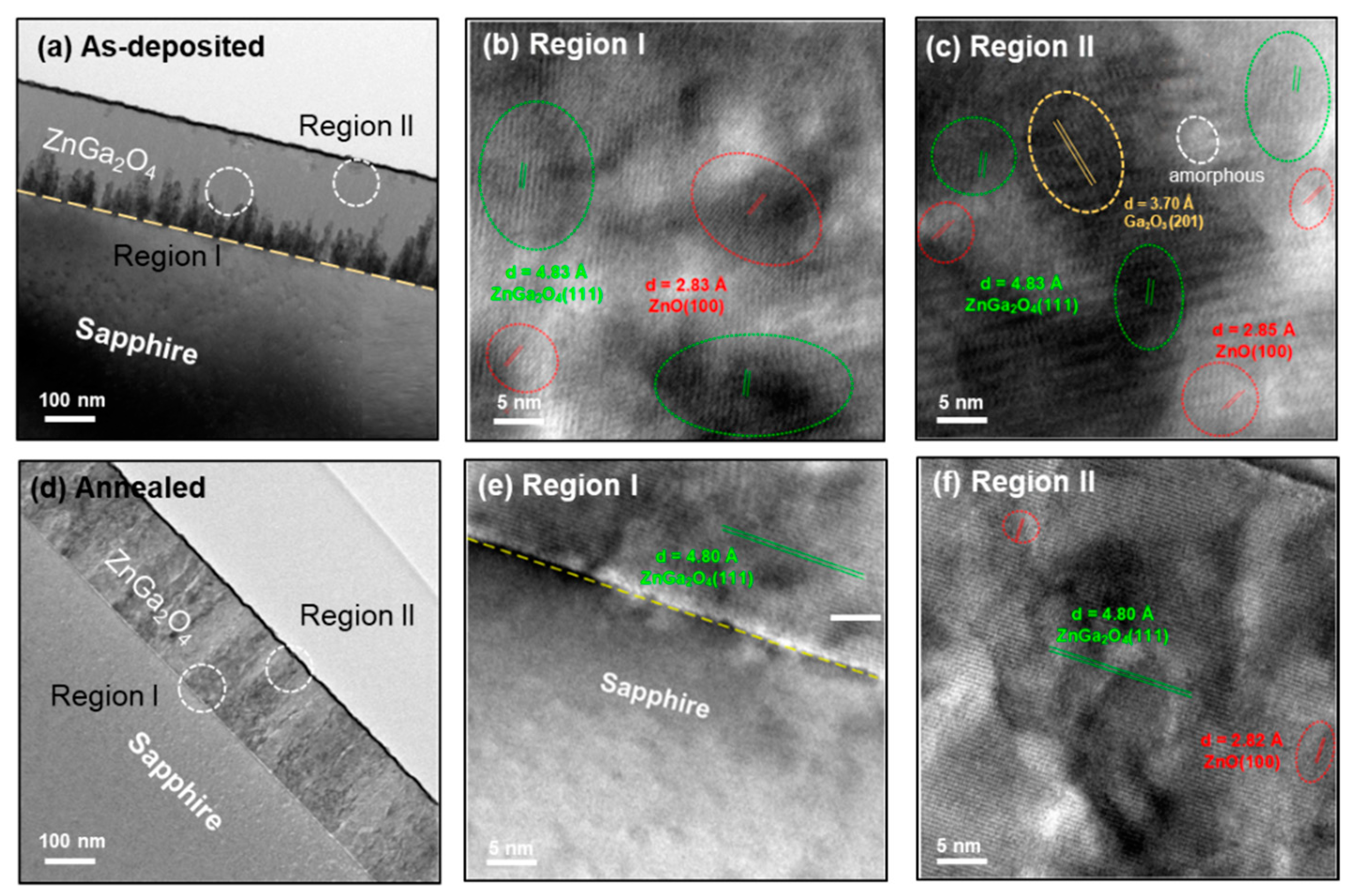
Figure 3 depicts the cross-sectional and high-resolution transmission electron micrographs (HRTEM) of as-deposited and annealed ZnGa
2O
4 film under air ambience. The cross-sectional TEM micrograph of as-deposited ZnGa
2O
4 film is shown in
Figure 3a, while region I and region II of this film are explored in
Figure 3b,c, respectively. This as-deposited ZnGa
2O
4 film demonstrated columnar grains near the substrate region and possessed the amorphous, ZnO (100), Ga
2O
3 (201), and ZnGa
2O
4 (111) phases. These phases are evident in this film, as it was deposited at a substrate temperature of 400 °C. The d-spacing of ~2.83, 3.70, and 4.83 Å (compatible with 4.80 Å) was measured, which corresponded to the ZnO (111), Ga
2O
3(201), and ZnGa
2O
4 (111) phases, respectively. The rapid thermal annealing was performed at the temperature of 700 ℃ for 1 min under air ambience to improve the crystallinity of this film. The oxygen present in the air ambience during thermal annealing played a significant role in eliminating the intrinsic defects, such as amorphous regions and oxygen vacancies in the films. A cross-sectional TEM micrograph of the annealed ZnGa
2O
4 film under air ambience is shown in
Figure 3d, and its region I and region II are explored in
Figure 3e,f, respectively. These regions (I and II) of the annealed ZnGa
2O
4 film demonstrated that rapid thermal annealing under air ambience suppressed the amorphous and Ga
2O
3 phases by the local bond rearrangement at the interface between the amorphous phase and the crystalline phase, and achieved a quasi-single-crystalline ZnGa
2O
4 structure, as shown in
Figure 3e,f.
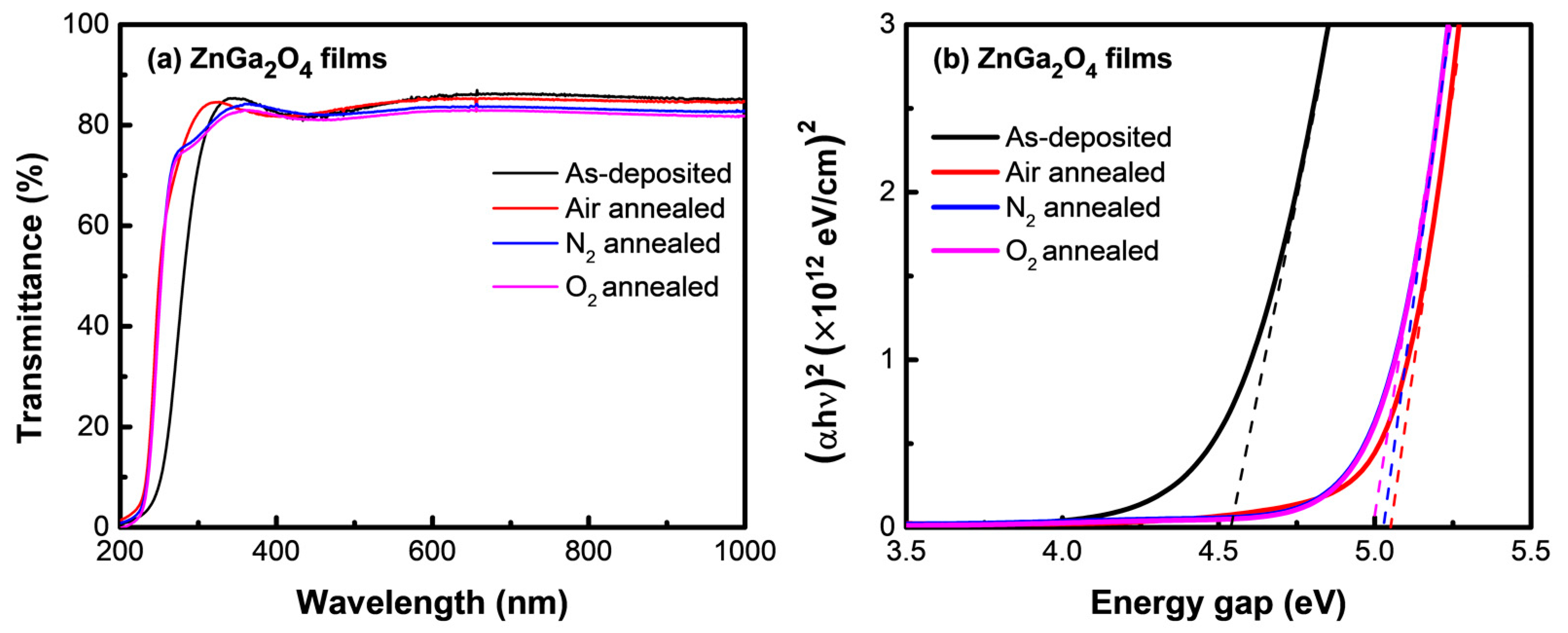
Figure 4a shows the transmittance spectrum of the as-deposited and annealed ZnGa
2O
4 films under different annealing ambiences. The average transmittance of the as-deposited and annealed ZnGa
2O
4 films was over 82% in the visible range, with a sharp cut-off in the DUV region. The absorption band-edge of the as-deposited film shifted to shorter wavelengths upon thermal annealing, which demonstrated the improvement in the optical characteristics of this film.
Figure 4b shows the Tauc plot, which demonstrates the bandgap values for the as-deposited and annealed ZnGa
2O
4 films under different ambiences. The transmittances values of these films were taken into consideration to calculate the absorption coefficient α. The optical bandgap of ZnGa
2O
4 films was obtained using the following relation:
where A, α, hν, and E
g represent the constant, absorption coefficient, energy of the incident photon, and the bandgap energy, respectively. The narrow bandgap of 4.53 eV in the as-deposited ZnGa
2O
4 film can be attributed to the existence of defect states (amorphous structure, phase separations between Ga
2O
3 and ZnO), as shown by TEM (see
Figure 3b,c). This led the excited electron to migrate to the conduction band with a low photon energy, narrowing the bandgap. Thermal annealing in various ambiences mitigates the defects (including amorphous nature and oxygen vacancies) that are common in as-deposited ZnGa
2O
4 film. As the thermal annealing was employed, the bandgap increased as 4.98, 5.02, and 5.05 eV under oxygen, nitrogen, and air ambiences, respectively, which allowed this material to lie within the DUV region. It is widely known that materials with a bandgap greater than 4.4 eV absorb UV-C radiation while ignoring visible light, making them ideal for use as high-sensitivity DUV PDs.
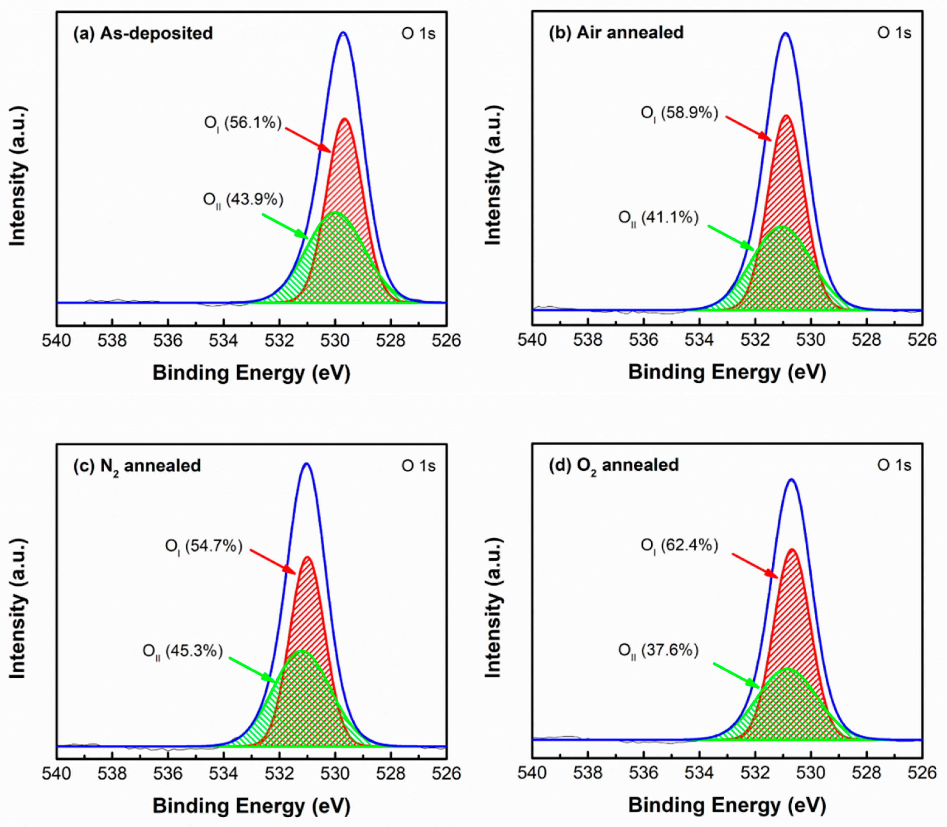
Figure 5 shows the O 1s XPS spectra of the as-deposited and annealed ZnGa
2O
4 films under different ambiences. In order to define the oxygen vacancies associated with the films, the O 1s XPS spectra of the films were fitted with the Gaussian function and deconvoluted into two peaks named O
I and O
II. The O
I peak centered around the lower binding energies of 530–531 eV represents the oxygen deficiency in the films, whereas the O
II peak centered at higher binding energies of 531–532 eV represents the oxygen vacancies in the film [
27]. The integrated areas of the O
II peak of the ZnGa
2O
4 films were found to be 43.9, 41.1, 45.3, and 37.6% for as-deposited, air annealed, N
2 annealed, and O
2 annealed ambiences, respectively. The oxygen present in the air ambience can fill a certain amount of oxygen vacancy. Hence, the area of O
II peak was found to be decreased from 43.9 to 41.1% during air annealing, as shown in
Figure 5b. The area of the O
II peak was found to be higher (45.3%) in an N
2 atmosphere, which can be attributed to the disassociation of oxygen molecules from the films during annealing. This resulted in an increased number of oxygen vacancies, as shown in
Figure 5c [
25]. By observing the integrated areas of O
II peaks from
Figure 5a–d, it was found that the O
2-annealed ZnGa
2O
4 film had the lowest integrated area of O
II peaks (37.6%). It is well-known that an oxygen-rich ambience reduces the number of oxygen vacancies, which weakens the crystalline structure [
28]. This phenomenon is in accordance with our XRD results, as shown in
Figure 1, where oxygen ambience deteriorated the crystalline structure. Since oxygen vacancies affect the optoelectronic properties of ZnGa
2O
4 film, the considerable suppression of oxygen vacancies demonstrates the tunability of the film characteristics depending on the annealing ambiences.
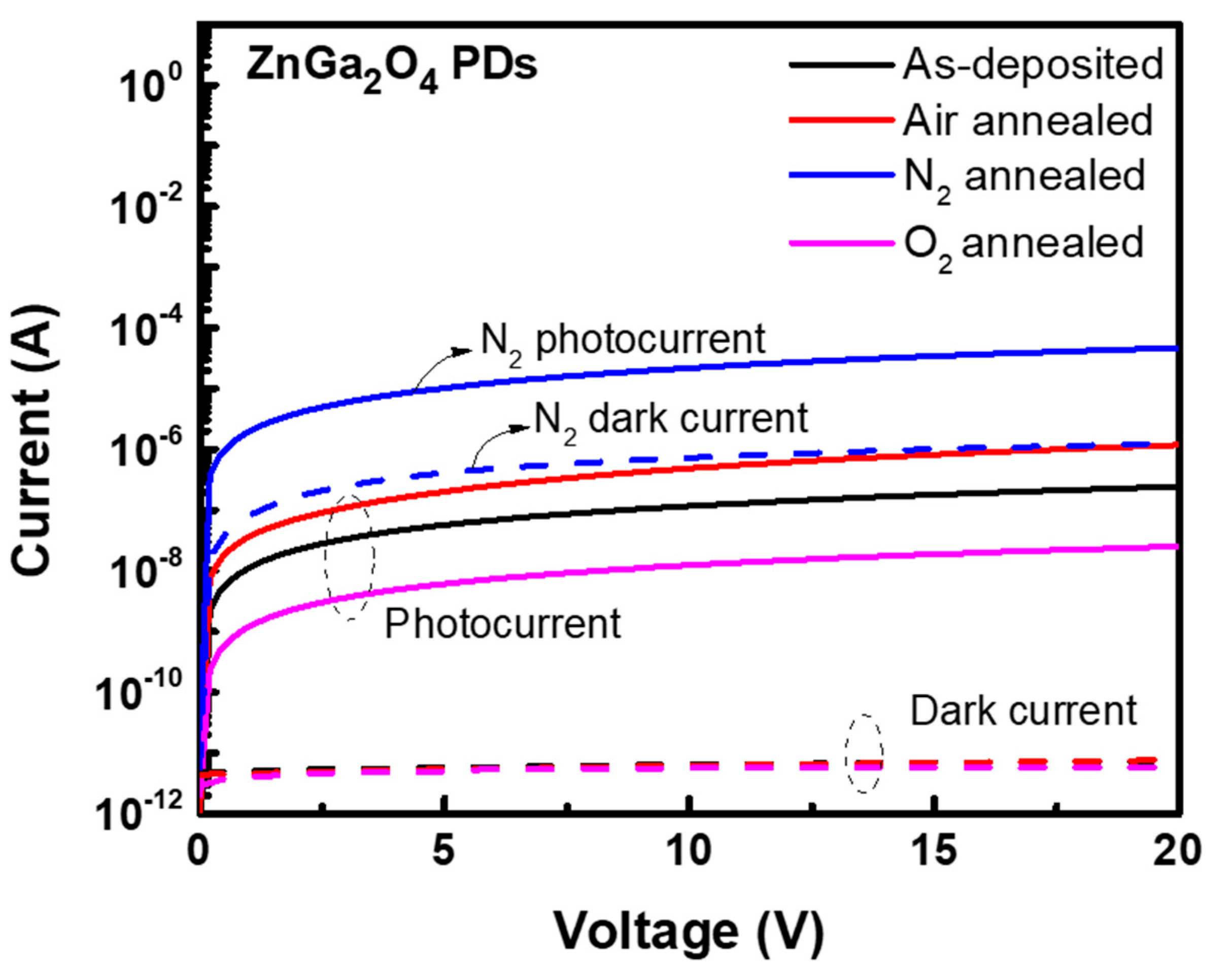
Figure 6 shows the I–V characteristics of the as-deposited and annealed ZnGa
2O
4 PDs under different annealing ambiences. The as-deposited ZnGa
2O
4 PD exhibited the photocurrent and dark current of 5.69 × 10
−8 A and 5.77 × 10
−12 A, respectively. This photocurrent had decreased from 5.69 × 10
−8 to 6.12 × 10
−9 A after annealing under oxygen ambience. This decreased photocurrent can be ascribed to the fulfilment of oxygen vacancies during high temperature annealing under oxygen ambience, which oxidized the ZnGa
2O
4 films and resulted in the decreased value of photocurrent. Nitrogen ambience caused the desorption of oxygen atoms from the surface of the films, and created oxygen vacancies, which drastically increased the photocurrent of the as-deposited ZnGa
2O
4 PD from 5.69 × 10
−8 to 9.64 × 10
−6 A. The dark current of as-deposited ZnGa
2O
4 PD was also found to be increased from 5.77 × 10
−12 to 3.33 × 10
−7 A upon annealing this film under nitrogen ambience, which was not desirable for PDs. This high dark current value can be attributed to the high number of inherent defects in the ZnGa
2O
4 PDs, such as oxygen vacancies and high surface density states, which can result in trapping states and was responsible for a higher internal gain. As a result, these surface states enhanced the dark current as well as the nonradiative recombination for the ZnGa
2O
4 film (annealed under nitrogen ambience). Similar results have been observed by Tsai et al. in their work [
29], where surface related defects were the main cause of the large leakage current in their device, which acted as the adsorption site and captured the free electrons in ZnGa
2O
4 films. When air ambience was used for annealing, ZnGa
2O
4 PD exhibited a photocurrent of 2.02 × 10
−7 A, a dark current of 5.35 × 10
−12 A, and a I
ph/I
dark of 3.77 × 10
4. Annealing ZnGa
2O
4 film under air ambience can fill a significant proportion of oxygen vacancies from the oxygen present in the air ambience, which exhibits the enhancement in optoelectronic characteristics of this ZnGa
2O
4 film and its potential to employ in DUV PDs.
Figure 7 shows the spectral response of the as-deposited and annealed ZnGa
2O
4 PDs under different annealing ambiences. The spectral response describes the sensitivity of the photodetector to optical radiation of various wavelengths, which is known as the responsivity of the photodetector. This parameter defines the performance of the photodetector and is represented by the following relation:
where I
ph is the photocurrent in Ampere (A), I
dark is the dark current in Ampere (A), and P
inc is the incident optical power in Watt (W). Hence, the responsivity of the photodetector is measured in A/W. As-deposited ZnGa
2O
4 PD possessed a responsivity of 0.71 A/W, which decreased to 0.12 A/W upon thermal annealing under oxygen ambience. This decreased responsivity could be due to the fulfilment of oxygen vacancies by oxygen gas, which further decreased the mobility of carriers and exhibited the poor responsivity of the ZnGa
2O
4 PD. Annealing under nitrogen ambience drastically increased the responsivity of ZnGa
2O
4 PD from 0.71 to 117 A/W. However, N
2 annealed ZnGa
2O
4 PD exhibited a broad spectral response from the DUV region to the visible region, which was not suitable for the DUV PDs. Annealing under nitrogen ambience reduced the oxygen concentration from the film and generated oxygen vacancy defects and surface density states. These defects led to the creation of deep-trapping centers, which increased the photocurrent as well as the dark current and enhanced the internal gain for ZnGa
2O
4 PD [
29]. Zheng et al. and Han et al. reported that the high responsivity of Mg
0.46Zn
0.54O and Mg
0.52Zn
0.48O films-based photodetectors is due to the long lifetime of photo-ionized holes, which were found to be trapped at the deep level. This measurement was precisely taken by using deep-level spectral measurement system in their works [
30,
31]. The trap states of holes include interface states between semiconductor and electrode, surface states, and deep level defects. These trap states were found responsible for this long lifetime phenomenon. It is clear that the photoresponse characteristics of ZnGa
2O
4 PDs could represent variations due to various oxygen vacancy related defects, which can be suppressed by the adaptation of air ambience. A large amount of oxygen molecules or atoms in the air ambience will diffuse into the samples and fill the significant number of oxygen vacancies, resulting in low surface density states [
32]. Annealing under air ambience exhibited both a significant enhancement in the photocurrent and reduction in the dark current by providing adequate energy to compensate the oxygen vacancy related defects. Hence, the responsivity of 2.53 A/W at the given bias of 5 V under the incident optical light of 240 nm was obtained for ZnGa
2O
4 PD under air ambience. The performance of our fabricated device is compared with that of the previously reported ZnGa
2O
4 PDs in
Table 1.
Figure 8 shows the rise time and fall time for the as-deposited and annealed ZnGa
2O
4 PDs under different annealing ambiences. Rise time is the time that the PD takes to change its response from 10% to 90% of the maximum photocurrent with the illumination of light. Fall time is the time that the PD takes to change its response from 90% to 10% of the maximum photocurrent without the illumination of light. These two characteristics (rise time and fall time) represent the response time of a photodetector. ZnGa
2O
4 PD annealed under air ambience possesses a higher rise time of 4.55 s but a lesser fall time of 0.19 s than other PDs (as-deposited, annealed ZnGa
2O
4 PDs under nitrogen and oxygen ambiences), which could be due to the indirect bandgap properties of the spinel-cubic ZnGa
2O
4 structure [
36]. The high rise time for the ZnGa
2O
4 PD annealed under air ambience could be attributed to the excitation of photogenerated carriers, which reached higher energy states above the conduction band. These excited photogenerated carriers then reverted to the conduction band by releasing energy and resulted in a high rise time. Despite the fact that the response time of ZnGa
2O
4 PDs annealed in air ambience is higher than that of other ZnGa
2O
4 PDs annealed under other ambiences, the responsivity associated with this air annealed ZnGa
2O
4 PD is found to be considerable for use in DUV PDs.


 ,
, 


