
Control of Ni/β-Ga2O3 Vertical Schottky Diode Output Parameters at Forward Bias by Insertion of a Graphene Layer


1
Laboratory of Semiconducting and Metallic Materials (LMSM), University of Biskra, Biskra 07000, Algeria
2
Department of Intelligent Mechatronics Engineering and Convergence Engineering for Intelligent Drone, Sejong University, Seoul 05006, Korea
*
Author to whom correspondence should be addressed.
Nanomaterials 2022, 12(5), 827; https://0-doi-org.brum.beds.ac.uk/10.3390/nano12050827
Submission received: 29 January 2022
/
Revised: 20 February 2022
/
Accepted: 26 February 2022
/
Published: 1 March 2022
(This article belongs to the Special Issue Carbon Nanostructures as Promising Future Materials)
Abstract
:Controlling the Schottky barrier height () and other parameters of Schottky barrier diodes (SBD) is critical for many applications. In this work, the effect of inserting a graphene interfacial monolayer between a Ni Schottky metal and a β- semiconductor was investigated using numerical simulation. We confirmed that the simulation-based on Ni workfunction, interfacial trap concentration, and surface electron affinity was well-matched with the actual device characterization. Insertion of the graphene layer achieved a remarkable decrease in the barrier height (), from 1.32 to 0.43 eV, and in the series resistance (), from 60.3 to 2.90. However, the saturation current () increased from to (A/cm2). The effects of a graphene bandgap and workfunction were studied. With an increase in the graphene workfunction and bandgap, the Schottky barrier height and series resistance increased and the saturation current decreased. This behavior was related to the tunneling rate variations in the graphene layer. Therefore, control of Schottky barrier diode output parameters was achieved by monitoring the tunneling rate in the graphene layer (through the control of the bandgap) and by controlling the Schottky barrier height according to the Schottky–Mott role (through the control of the workfunction). Furthermore, a zero-bandgap and low-workfunction graphene layer behaves as an ohmic contact, which is in agreement with published results.
Keywords:
SBD; β-Ga2O3; electron-beam evaporation; interfacial traps; graphene; workfunction; bandgap1. Introduction
Gallium oxide (Ga2O3) is a new oxide semiconductor material with a long and rich history [1,2]. Pioneer studies were performed in the 1960s but were almost forgotten for about three decades. However, in the last two decades, its ultra-wide bandgap (UWBG) of ~4.8 eV, high breakdown electric field of ~8 MV/cm, and high saturation velocity of have brought Ga2O3 to the fore again [3,4,5]. Ga2O3 has six polymorphs: α, β, γ, δ, ε and k, with β- being the most stable [4]. Furthermore, it can be grown directly from the melt at a low cost and allows for large-scale production compared with GaN, InGaN, and SiC [1,2,4]. However, this material has a problem with developing a stable p-type [2,5,6,7]. As a result, its use in bipolar devices is limited to a heterojunction with other p-type materials such as NiO [8,9] and Cu2O [10]. β-Ga2O3 is therefore mainly used in unipolar devices (SBD [4,11], MOSFET [12], Thin-Film Transistor (TFT) [13], and field emission [14] devices). The SBD device based on a UWBG semiconductor is of great interest and, aimed to improve the thermal stability and decrease the series resistance (), ideality factor (), and leakage current. A low threshold voltage () is preferred in order to minimize heating during prolonged device operation [15]. In addition to the above-mentioned characteristics, researchers aimed to develop SBDs with a controllable Schottky barrier height (), with the aim of developing SBD-based switching devices for special applications. According to the Schottky–Mott relation [16], the linear relation between the metal workfunction () and can be set to (). However, in most materials, this relation is not realistic due to unexpected effects such as the formation of interface states or an interface dipole [16]. Farzana et al. [17] studied the influence of the choice of metal in a (010) β- SBD. They used different metals, namely Pd, Ni, Pt, and Au, with a workfunction of 5.20, 5.25, 5.65, and 5.30 eV, respectively, and obtained for each metal an of 1.27, 1.54, 1.58, and 1.71 eV, respectively. After linking the metal workfunction values and the obtained , a modified Schottky–Mott relation for Au was obtained. Yao et al. [18] used W, Cu, Ni, Ir, and Pt with workfunctions of 4.55, 4.65, 5.15, 5.27, and 5.65 eV, respectively, and the corresponding values from the capacitance voltage were 1.94, 1.61, 1.61, 2.3, and 1.9 eV, respectively. It was also observed that does not show a universal trend with the metal workfunction, indicating that surface/interface states can play a very important role in determining an effective value. This is due to defects and the crystal orientation, crystal quality, and passivation with different types of surface treatments or metal deposition techniques. Among the different solutions that have been proposed to address these issues is depositing a layer with known properties between the metal and the β- that can improve the SBD’s performance and allow for better control. Bhattacharyya et al. [19] studied the modulation and enhancement of for different β- orientations and metals when an ultra-thin layer is inserted at the metal–β- interface. Harada et al. [15] reported systematic variations in in a metal/β- SBD while increasing the thickness of the inserted layer; the obtained results demonstrated good control of in a wide range (0.7 to 1.9 eV).
In this article, a new approach is proposed to improve and control the Schottky barrier height and other parameters of Ni/β- by inserting a graphene layer at the interface between the Ni and the β- so that the outputs of the SBD are controlled by the tunneling rate through the graphene layer (by tuning the graphene bandgap) and by the barrier between the graphene and the β- (by tuning the graphene workfunction).
2. Experimental
A β-Ga2O3 Schottky barrier diode (SBD) based on an epitaxial Si-doped (001) β-Ga2O3 drift layer was deposited on a Sn-doped (001) β-Ga2O3 substrate by halide vapor-phase epitaxy (HVPE). A nickel film was deposited on the drift layer using an electron-beam evaporation method followed by annealing at 400 °C. A schematic illustration of the SBD structure is shown in Figure 1. The thickness of the nickel, Si-doped β-Ga2O3, and Sn-doped β-Ga2O3 was 0.3, 10, and , respectively, while the doping was and , respectively. For more details, see our previous publication [20].
3. Simulation Methodology
SILVACO ATLAS TCAD software (License Number 14556 License Period 18-3-21 to 17-3-22, Biskra Université Laboratory of Metallic and Semiconducting Materials FSESNV, Biskra, Algeria) was used in this simulation to solve the basic drift-diffusion semiconductor equations, which are the Poisson and continuity equations.
The Poisson equation is given by [2,21]:
where is the electrostatic potential, is the permittivity, and are the free holes and electron concentrations, respectively, and is the trap’s ionized density .
The continuity equations for electrons and holes are defined in steady states by [2,21]:
where and are the generation rates for electrons and holes, respectively, and are the recombination rates for electrons and holes, respectively, and are the electron and hole current densities, respectively, which are given in terms of the quasi-Fermi level ( and ) and mobility ( and ) as [2,21]:
Traps are represented by their ionized density . The sign depends on whether the trap is an acceptor or a donor so that and , where is the occupancy function given by and is the trap capture cross-section for electrons (holes). Furthermore, the recombination rate is related to traps through the well-known SRH formula with and . and are the minority carrier lifetimes, which are also related to traps through , where is the thermal velocity of electrons (holes). The external generation rate is neglected since the forward bias is within low injection levels [2]. The tunneling mechanism through graphene, which has an important effect [22,23], has to be considered together with thermionic emissions, Shockley–Read–Hall and Auger recombination, Klassen’s concentration and mobility-dependent temperature, and a reduction in the image force in the simulation. For the graphene layer’s simulation, we considered this layer to be an ultra-thin (0.34 nm thickness) semiconductor with high mobilities, a low tunneling mass, and a low bandgap (0–0.45 eV). The dominant transport mechanism of electrons from Ni to graphene is a tunneling mechanism. Tunnelling was considered by using the Universal Schottky Tunnelling (UST) model and the tunnelling current is given by [7]:
where , , , ϵ, , and are the effective Richardson’s coefficient (41.11 for β-Ga2O3 [2]), the lattice temperature, the Boltzmann constant, the electron energy, and the Maxwell–Boltzmann distribution in the semiconductor and metal, respectively, and is the tunnelling probability given by [7]:
where , (, and are the potential energy distribution of the Schottky barrier diode, the classical turning points, and the tunnelling mass in graphene (= 0.012m0 where m0 is the free electron mass [24]), respectively. In addition, the thermionic emission plays an important role in this type of device. The properties and traps related to each layer are presented in Table 1 and Table 2, respectively.
4. Results
As presented in Figure 2, a good comparison between the simulation data and the experimental measurements was obtained. The extracted Ni workfunction, interfacial trap concentrations, and surface electron affinity from SILVACO ATLAS software were 5 eV, for all traps ( (), (), and ()), and eV, respectively.
4.1. Effect of Insertion of a Graphene Layer
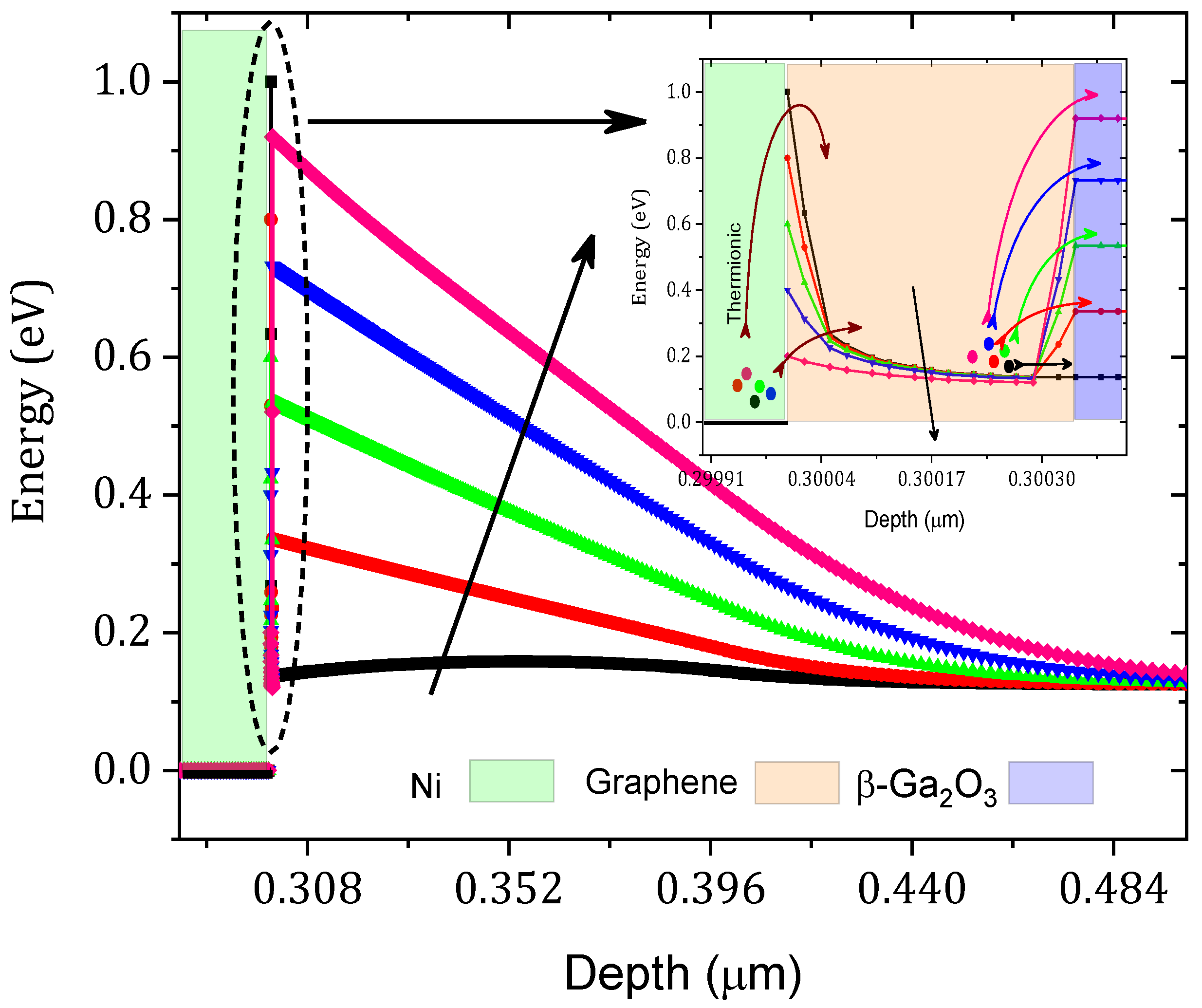
The main goal of the present work was to study the effect of inserting a graphene monolayer between the Ni and the . This monolayer has the potential ability to come into contact with the at a low Schottky barrier height. As shown in Figure 3, a strong effect on the forward current and a reduction in the Schottky barrier height from 1.32 to 0.43 eV were obtained. These results are in agreement with those of Yuan et al. [27], where a very low was obtained. The results are also in agreement with those of Zhong et al. [28], who found a decrease in when a graphene layer was inserted into a GaN SBD. According to Courtin et al. [22], a similar variation for a graphene–silicon interface was obtained. Inaba et al. [29] also found a very low at a CNT–SiC interface. In addition, a decrease in the series resistance () from 60.3 to 2.90 was obtained. However, an increase in the saturation current from to (A/cm2) was observed after the insertion of this graphene layer. This decrease in and along with the increase in the saturation current when the graphene monolayer was inserted can be explained by the increase in the tunneling rate, especially at the interface between the Ni and the graphene as shown in Figure 4. Accordingly, for the electron transport from the Ni to the graphene layer (assuming sufficient energy to overcome the barrier), the thermionic emission dominated. Otherwise, when the electron energy was lower than the barrier energy, tunneling played an important role, especially at the Ni–graphene interface.
With the graphene layer, the tunneling mechanism increased the density of the extracted free electrons from the Ni to the graphene and then to the β- by the thermionic emission and tunneling. This led to a large decrease in . In addition, electron tunneling through the formed barriers between Ni/graphene and graphene/β- affected the SBD parameters.
4.2. Graphene Bandgap Effect
We demonstrated that a graphene monolayer can enhance the SBD outputs by increasing the tunneling rate. Experimentally, the graphene bandgap can be controlled by several methods. Takahashi et al. [30] found that the bandgap gradually increases with oxygen adsorption to as high as 0.45 eV upon exposure to 2000 L of oxygen. Additionally, the bandgap can be increased by atomic and molecular doping control, such as the simultaneous insertion of holes and electrons at hetero sites [31]. Altering the number of graphene layers is another way of tuning the graphene bandgap [32]. Bearing in mind these facts, the effect of the graphene bandgap was investigated and, as shown in Figure 5, as the graphene bandgap increased from 0 to 0.45 eV, the output current was affected.
The value increased from 0.43 eV to 0.69 eV and the series resistance increased from 2.90 to 5.90 mΩ cm2 as shown in Figure 6. This result can be interpreted as a decrease in the tunneling rate, as shown in Figure 7. This decrease in the tunneling rate is related to the increase in the potential energy distribution of the Schottky barrier diode as presented in Figure 8. A high tunneling rate was obtained in most cases at the Ni–graphene interface that was higher than that at the graphene–β- interface. The obtained values demonstrate the possibility of tuning the Schottky barrier height of a Ni–β- Schottky diode through the control of the tunneling rate in the graphene layer. Figure 8 shows the conduction band variation for the Ni/graphene/β- SBD with an increasing graphene bandgap. The barrier between the Ni and the graphene increased and this affected the electron tunneling from the Ni to the graphene. In addition, a small increase in the barrier between the graphene and the β- was observed and this led to an increase in .
4.3. Graphene Workfunction Effect
The effect of the graphene workfunction on SBD parameters was investigated. In this study, a zero-bandgap graphene layer was considered. As the graphene workfunction increased from 4 to 4.8 eV, the output current was affected (Figure 9) and increased from 0.320 eV to 0.545 eV as presented in Figure 10. This increase in can be interpreted according to the simple Schottky–Mott model as the difference between the workfunction of graphene () and the affinity of β-() [22]:
Furthermore, a decrease in the saturation current was obtained with the increase in the graphene workfunction.
As the graphene workfunction increased, increased from 0.89 to 3.9 mΩ.cm2. This is related to the decrease in the tunneling rate in the graphene layer. Generally, controlling the graphene workfunction means controlling between the graphene and the β- as presented in Figure 11. As the workfunction increases, the barrier between the graphene and the β- increases while that between the Ni and the graphene decreases. This leads to a decrease in the number of electrons transported from the graphene to the β- by thermionic emission. Therefore, an increase in and a decrease in the saturation current were obtained with an increase in the graphene workfunction. Experimentally and as described in [31,32], the graphene workfunction can be controlled by altering the number of graphene layers. The workfunction increased as well, reaching 4.8 eV. In addition, altering the graphene doping density is an essential method for controlling the graphene workfunction because doping the graphene layer changes the fermi-level of the graphene, which affects the electronic properties of the graphene and, among the properties, the workfunction [33,34]. In addition, a zero-bandgap and low-workfunction SBD behaves as an ohmic contact as shown in the inset of Figure 9 (the current has a linear variation versus the forward voltage). Figure 11 shows the equilibrium band diagram. For a low workfunction (4 eV), a very low barrier is formed between the graphene and the β-. It was therefore concluded that a graphene layer with a lower workfunction (4 eV) and a 0-eV bandgap transitioned from a Schottky contact to an ohmic contact. This result is in agreement with the simulation result obtained by Yuan et al. [27].
5. Conclusions
In summary, this study investigated the effect of a graphene layer on characteristics of a Ni/β- SBD. Firstly, good agreement between simulation data and experimental measurements was obtained for the Ni/β- SBD without a graphene layer with the consideration of a 5 eV Ni workfunction, an density for the (), (), and () interfacial traps, and a eV surface electron affinity. Then, the effect of inserting a zero-bandgap graphene layer at the interface between the Ni and the β- was studied. We observed a decrease in both and the series resistance . However, the saturation current n increased. These effects were related to an increase in the tunneling rate. The graphene bandgap and workfunction were used to control the output parameters of the SBD. When the graphene bandgap increased, the Schottky barrier height and series resistance both increased. Similarly, and increased as well. In addition, with a lower graphene workfunction, Ni behaved as an ohmic contact with β-.
Author Contributions
Software and writing—original draft preparation, M.L.; investigation and writing—review and editing, N.S.; writing—review and editing, Y.S.R. All authors have read and agreed to the published version of the manuscript.
Funding
This work was supported by the National Research Foundation of Korea (NRF) grant funded by the Korea government (MSIT) (No. 2020R1A2C1013693) and was also supported by the Technology Innovation Program-(20016102, Development of 1.2 kV Gallium oxide power semiconductor devices technology) funded by the Ministry of Trade, Industry, and Energy (MOTIE, Korea).
Conflicts of Interest
The authors declare that they have no known competing financial interests or personal relationships that could have influenced the work reported in this paper.
References
- Xue, H.; He, Q.; Jian, G.; Long, S.; Pang, T.; Liu, M. An Overview of the Ultrawide Bandgap Ga2O3 Semiconductor-Based Schottky Barrier Diode for Power Electronics Application. Nanoscale Res. Lett. 2018, 13, 290. [Google Scholar] [CrossRef] [PubMed] [Green Version]
- Labed, M.; Sengouga, N.; Labed, M.; Meftah, A.; Kyoung, S.; Kim, H.; Rim, Y.S. Modeling a Ni/β-Ga2O3 Schottky barrier diode deposited by confined magnetic-field-based sputtering. J. Phys. D Appl. Phys. 2021, 54, 115102. [Google Scholar] [CrossRef]
- Polyakov, A.Y.; Lee, I.-H.; Smirnov, N.B.; Yakimov, E.B.; Shchemerov, I.V.; Chernykh, A.V.; Kochkova, A.I.; Vasilev, A.A.; Carey, P.H.; Ren, F.; et al. Defects at the surface of β-Ga2O3 produced by Ar plasma exposure. APL Mater. 2019, 7, 061102. [Google Scholar] [CrossRef] [Green Version]
- Galazka, Z. β-Ga2O3 for wide-bandgap electronics and optoelectronics. Semicond. Sci. Technol. 2018, 33, 113001. [Google Scholar] [CrossRef]
- Kyrtsos, A.; Matsubara, M.; Bellotti, E. On the feasibility of p-type Ga2O3. Appl. Phys. Lett. 2018, 112, 032108. [Google Scholar] [CrossRef]
- Chikoidze, E.; Sartel, C.; Mohamed, H.; Madaci, I.; Tchelidze, T.; Modreanu, M.; Vales-Castro, P.; Rubio, C.; Arnold, C.; Sallet, V.; et al. Enhancing the intrinsic p-type conductivity of the ultra-wide bandgap Ga2O3 semiconductor. J. Mater. Chem. C 2019, 7, 10231–10239. [Google Scholar] [CrossRef]
- Labed, M.; Sengouga, N.; Meftah, A.; Labed, M.; Kyoung, S.; Kim, H.; Rim, Y.S. Leakage Current Modelling and Optimization of β-Ga2O3 Schottky Barrier Diode with Ni Contact under High Reverse Voltage. ECS J. Solid State Sci. Technol. 2020, 9, 125001. [Google Scholar] [CrossRef]
- Kokubun, Y.; Kubo, S.; Nakagomi, S. All-oxide p–n heterojunction diodes comprising p-type NiO and n-type β-Ga2O3. Appl. Phys. Express 2016, 9, 91101. [Google Scholar] [CrossRef]
- Gong, H.; Zhou, F.; Xu, W.; Yu, X.; Xu, Y.; Yang, Y.; Ren, F.; Gu, S.; Zheng, Y.; Zhang, R.; et al. 1.37 kV/12 A NiO/β-Ga2O3 Heterojunction Diode With Nanosecond Reverse Recovery and Rugged Surge-Current Capability. IEEE Trans. Power Electron. 2021, 36, 12213–12217. [Google Scholar] [CrossRef]
- Watahiki, T.; Yuda, Y.; Furukawa, A.; Yamamuka, M.; Takiguchi, Y.; Miyajima, S. Heterojunction p-Cu2O/n-Ga2O3 diode with high breakdown voltage. Appl. Phys. Lett. 2017, 111, 222104. [Google Scholar] [CrossRef]
- Jian, G.; He, Q.; Mu, W.; Fu, B.; Dong, H.; Qin, Y.; Zhang, Y.; Xue, H.; Long, S.; Jia, Z.; et al. Characterization of the inhomogeneous barrier distribution in a Pt/(100) β-Ga2O3 Schottky diode via its temperature-dependent electrical properties. AIP Adv. 2018, 8, 015316. [Google Scholar] [CrossRef] [Green Version]
- Pearton, S.J.; Ren, F.; Tadjer, M.; Kim, J. Perspective: Ga2O3 for ultra-high power rectifiers and MOSFETS. J. Appl. Phys. 2018, 124, 220901. [Google Scholar] [CrossRef] [Green Version]
- Thomas, S.R.; Adamopoulos, G.; Lin, Y.-H.; Faber, H.; Sygellou, L.; Stratakis, E.; Pliatsikas, N.; Patsalas, P.A.; Anthopoulos, T.D. High electron mobility thin-film transistors based on Ga2O3 grown by atmospheric ultrasonic spray pyrolysis at low temperatures. Appl. Phys. Lett. 2014, 105, 092105. [Google Scholar] [CrossRef]
- Grillo, A.; Barrat, J.; Galazka, Z.; Passacantando, M.; Giubileo, F.; Iemmo, L.; Luongo, G.; Urban, F.; Dubourdieu, C.; Di Bartolomeo, A. High field-emission current density from β-Ga2O3 nanopillars. Appl. Phys. Lett. 2019, 114, 193101. [Google Scholar] [CrossRef]
- Harada, T.; Tsukazaki, A. Control of Schottky barrier height in metal/β-Ga2O3 junctions by insertion of PdCoO2 layers. APL Mater. 2020, 8, 41109. [Google Scholar] [CrossRef] [Green Version]
- Tung, R.T. The physics and chemistry of the Schottky barrier height. Appl. Phys. Rev. 2014, 1, 11304. [Google Scholar] [CrossRef] [Green Version]
- Farzana, E.; Zhang, Z.; Paul, P.K.; Arehart, A.R.; Ringel, S.A. Influence of metal choice on (010) β-Ga2O3 Schottky diode properties. Appl. Phys. Lett. 2017, 110, 202102. [Google Scholar] [CrossRef]
- Yao, Y.; Gangireddy, R.; Kim, J.; Das, K.K.; Davis, R.F.; Porter, L.M. Electrical behavior of β-Ga2O3 Schottky diodes with different Schottky metals. J. Vac. Sci. Technol. B Nanotechnol. Microelectron. Mater. Process. Meas. Phenom. 2017, 35, 03D113. [Google Scholar] [CrossRef]
- Bhattacharyya, A.; Ranga, P.; Saleh, M.; Roy, S.; Scarpulla, M.A.; Lynn, K.G.; Krishnamoorthy, S. Schottky Barrier Height Engineering in β-Ga2O3 Using SiO2 Interlayer Dielectric. IEEE J. Electron Devices Soc. 2020, 8, 286–294. [Google Scholar] [CrossRef]
- Kim, H.; Kyoung, S.; Kang, T.; Kwon, J.Y.; Kim, K.H.; Rim, Y.S. Effective surface diffusion of nickel on single crystal β-Ga2O3 for Schottky barrier modulation and high thermal stability. J. Mater. Chem. C 2019, 7, 10953–10960. [Google Scholar] [CrossRef]
- Labed, M.; Sengouga, N.; Meftah, A.; Meftah, A.; Rim, Y.S. Study on the improvement of the open-circuit voltage of NiOx/Si heterojunction solar cell. Opt. Mater. 2021, 120, 111453. [Google Scholar] [CrossRef]
- Courtin, J.; Le Gall, S.; Chrétien, P.; Moréac, A.; Delhaye, G.; Lépine, B.; Tricot, S.; Turban, P.; Schieffer, P.; Le Breton, J.-C. A low Schottky barrier height and transport mechanism in gold–graphene–silicon (001) heterojunctions. Nanoscale Adv. 2019, 1, 3372–3378. [Google Scholar] [CrossRef] [Green Version]
- Zhu, X.; Lei, S.; Tsai, S.-H.; Zhang, X.; Liu, J.; Yin, G.; Tang, M.; Torres, C.M.; Navabi, A.; Jin, Z.; et al. A Study of Vertical Transport through Graphene toward Control of Quantum Tunneling. Nano Lett. 2018, 18, 682–688. [Google Scholar] [CrossRef] [PubMed]
- Tiras, E.; Ardali, S.; Tiras, T.; Arslan, E.; Cakmakyapan, S.; Kazar, O.; Hassan, J.; Janzén, E.; Ozbay, E. Effective mass of electron in monolayer graphene: Electron-phonon interaction. J. Appl. Phys. 2013, 113, 43708. [Google Scholar] [CrossRef]
- Dadashbeik, M.; Fathi, D.; Eskandari, M. Design and simulation of perovskite solar cells based on graphene and TiO2/graphene nanocomposite as electron transport layer. Sol. Energy 2020, 207, 917–924. [Google Scholar] [CrossRef]
- Labed, M.; Sengouga, N.; Labed, M.; Meftah, A.; Kyoung, S.; Kim, H.; Rim, Y.S. Modeling and analyzing temperature-dependent parameters of Ni/β-Ga2O3 Schottky barrier diode deposited by confined magnetic field-based sputtering. Semicond. Sci. Technol. 2021, 36, 35020. [Google Scholar] [CrossRef]
- Yuan, H.; Su, J.; Guo, R.; Tian, K.; Lin, Z.; Zhang, J.; Chang, J.; Hao, Y. Contact barriers modulation of graphene/β-Ga2O3 interface for high-performance Ga2O3 devices. Appl. Surf. Sci. 2020, 527, 146740. [Google Scholar] [CrossRef]
- Zhong, H.; Xu, K.; Liu, Z.; Xu, G.; Shi, L.; Fan, Y.; Wang, J.; Ren, G.; Yang, H. Charge transport mechanisms of graphene/semiconductor Schottky barriers: A theoretical and experimental study. J. Appl. Phys. 2014, 115, 13701. [Google Scholar] [CrossRef]
- Inaba, M.; Suzuki, K.; Shibuya, M.; Lee, C.-Y.; Masuda, Y.; Tomatsu, N.; Norimatsu, W.; Hiraiwa, A.; Kusunoki, M.; Kawarada, H. Very low Schottky barrier height at carbon nanotube and silicon carbide interface. Appl. Phys. Lett. 2015, 106, 123501. [Google Scholar] [CrossRef]
- Takahashi, T.; Sugawara, K.; Noguchi, E.; Sato, T.; Takahashi, T. Band-gap tuning of monolayer graphene by oxygen adsorption. Carbon N. Y. 2014, 73, 141–145. [Google Scholar] [CrossRef]
- Hussain, A.; Ullah, S.; Farhan, M.A. Fine tuning the band-gap of graphene by atomic and molecular doping: A density functional theory study. RSC Adv. 2016, 6, 55990–56003. [Google Scholar] [CrossRef]
- Xu, X.; Liu, C.; Sun, Z.; Cao, T.; Zhang, Z.; Wang, E.; Liu, Z.; Liu, K. Interfacial engineering in graphene bandgap. Chem. Soc. Rev. 2018, 47, 3059–3099. [Google Scholar] [CrossRef] [PubMed]
- Hibino, H.; Kageshima, H.; Kotsugi, M.; Maeda, F.; Guo, F.-Z.; Watanabe, Y. Dependence of electronic properties of epitaxial few-layer graphene on the number of layers investigated by photoelectron emission microscopy. Phys. Rev. B 2009, 79, 125437. [Google Scholar] [CrossRef]
- Naghdi, S.; Sanchez-Arriaga, G.; Rhee, K.Y. Tuning the work function of graphene toward application as anode and cathode. J. Alloys Compd. 2019, 805, 1117–1134. [Google Scholar] [CrossRef] [Green Version]
Figure 1.
A schematic of the structure of the Ni/β-Ga2O3 SBD studied in this work.

Figure 2.
Comparison between the simulation data and experimental measurements. The inset is a linear representation of the J-V characteristics.
Figure 2.
Comparison between the simulation data and experimental measurements. The inset is a linear representation of the J-V characteristics.

Figure 3.
The effect of the insertion of a graphene layer on the forward current.

Figure 4.
Variation in the tunneling rate when a graphene monolayer was inserted under 2 V of forward voltage.
Figure 4.
Variation in the tunneling rate when a graphene monolayer was inserted under 2 V of forward voltage.

Figure 5.
Output J-V variations with the graphene bandgap.

Figure 6.
Variation in the output parameters of the proposed SBD versus the graphene bandgap.

Figure 7.
Variation in the tunneling rate versus the graphene bandgap under 2 V of forward voltage.

Figure 8.
Equilibrium conduction band variation with the graphene workfunction. The inset is a zoomed Ni/graphene/ β- interface conduction band.
Figure 8.
Equilibrium conduction band variation with the graphene workfunction. The inset is a zoomed Ni/graphene/ β- interface conduction band.

Figure 9.
Output J-V variation versus the graphene workfunction. The inset is a linear representation of the J-V characteristics.
Figure 9.
Output J-V variation versus the graphene workfunction. The inset is a linear representation of the J-V characteristics.

Figure 10.
Variation in the output parameters of the proposed SBD versus the graphene workfunction.

Figure 11.
Variation in the equilibrium conduction band with the graphene workfunction. The inset is a zoomed Ni/graphene/β- interface conduction band.
Figure 11.
Variation in the equilibrium conduction band with the graphene workfunction. The inset is a zoomed Ni/graphene/β- interface conduction band.


| Parameters | Sn: β-Ga2O3 | Si: β-Ga2O3 | Graphene |
|---|---|---|---|
| Bandgap (eV) | 4.8 | 4.8 | 0–0.45 |
| Affinity (eV) | 4 | 4 | 4–4.8 |
| 10 | 10 | 9000 | |
| 172 | 300 | 9000 | |
| Relative permittivity | 12.6 | 11 | 6.9 |
| / | |||
| Thickness (µm) | 650 | 10 | 0.34 × 10⁻³ |
Publisher’s Note: MDPI stays neutral with regard to jurisdictional claims in published maps and institutional affiliations. |
© 2022 by the authors. Licensee MDPI, Basel, Switzerland. This article is an open access article distributed under the terms and conditions of the Creative Commons Attribution (CC BY) license (https://creativecommons.org/licenses/by/4.0/).
Share and Cite
MDPI and ACS Style
Labed, M.; Sengouga, N.; Rim, Y.S. Control of Ni/β-Ga2O3 Vertical Schottky Diode Output Parameters at Forward Bias by Insertion of a Graphene Layer. Nanomaterials 2022, 12, 827. https://0-doi-org.brum.beds.ac.uk/10.3390/nano12050827
AMA Style
Labed M, Sengouga N, Rim YS. Control of Ni/β-Ga2O3 Vertical Schottky Diode Output Parameters at Forward Bias by Insertion of a Graphene Layer. Nanomaterials. 2022; 12(5):827. https://0-doi-org.brum.beds.ac.uk/10.3390/nano12050827
Chicago/Turabian StyleLabed, Madani, Nouredine Sengouga, and You Seung Rim. 2022. "Control of Ni/β-Ga2O3 Vertical Schottky Diode Output Parameters at Forward Bias by Insertion of a Graphene Layer" Nanomaterials 12, no. 5: 827. https://0-doi-org.brum.beds.ac.uk/10.3390/nano12050827
Note that from the first issue of 2016, this journal uses article numbers instead of page numbers. See further details here.