
Characterization of Magnetron Sputtered BiTe-Based Thermoelectric Thin Films


1
School of Metallurgy and Materials, The University of Birmingham, Birmingham B15 2TT, UK
2
Cavendish Laboratory, University of Cambridge, Cambridge CB3 0HE, UK
3
Design, Manufacturing and Engineering Management, University of Strathclyde, Glasgow G1 1XQ, UK
*
Author to whom correspondence should be addressed.
Nanomaterials 2023, 13(1), 208; https://0-doi-org.brum.beds.ac.uk/10.3390/nano13010208
Submission received: 15 December 2022
/
Revised: 26 December 2022
/
Accepted: 29 December 2022
/
Published: 3 January 2023
(This article belongs to the Special Issue Nanostructured Materials for Energy Applications)
Abstract
:Thermoelectric (TE) technology attracts much attention due to the fact it can convert thermal energy into electricity and vice versa. Thin-film TE materials can be synthesized on different kinds of substrates, which offer the possibility of the control of microstructure and composition to higher TE power, as well as the development of novel TE devices meeting flexible and miniature requirements. In this work, we use magnetron sputtering to deposit N-type and P-type BiTe-based thin films on silicon, glass, and Kapton HN polyimide foil. Their morphology, microstructure, and phase constituents are studied by SEM/EDX, XRD, and TEM. The electrical conductivity, thermal conductivity, and Seebeck coefficient of the thin film are measured by a special in-plane advanced test system. The output of electrical power (open-circuit voltage and electric current) of the thin film is measured by an in-house apparatus at different temperature gradient. The impact of deposition parameters and the thickness, width, and length of the thin film on the power output are also investigated for optimizing the thin-film flexible TE device to harvest thermal energy.
1. Introduction
In the past decades, extensive research on renewable energy has witnessed a significant advance in harvesting thermal energy into electricity via different pathways to maximize the Seebeck coefficient (S), the electrical conductivity (σ), and the reduction in the thermal conductivity (κ) [1]. The progress of the conventional heavy-atom-doped semiconductors, such as Bi2Te3, PbTe, Si–Ge, and Te–Ag–Ge–Sb, has resulted in increased thermoelectric figure of merit (ZT), which makes the technology more efficient at producing power [2]. To overcome the deficit of rare elements such as tellurium and avoid hazardous elements such as lead, alternative materials, such as bismuth sulfide (Bi2S3) [3], tin selenide (SnSe) [4], and magnesium-silicon-based new materials [5], have attracted much attention, and higher performance reports emerge regularly. However, the properties of bulk TE materials are determined primarily by composition and microstructure, which limits the usage of thermoelectric energy conversion to niche applications. Furthermore, bulk TE materials are limited by shape and size, which restricts their application in the area of intelligent and flexible TE devices. In contrast, thin-film technology has an advantage in controlling the composition, thickness, and microstructure, and higher TE power can be realized by quantum effects and band-gap engineering using reduced-dimensionality materials [6]. The nanosized structure results in the presence of a large number of interfaces (grain boundaries), which may effectively scatter phonons and thus reduce the thermal conductivity considerably and lead to a substantial increase in thermopower [7]. In the meantime, diversified substrates, for example, polymers, can be used to meet the flexible, lightweight, and miniature requirements [8].
Different film-growth methods based on molecular-beam epitaxy (MBE) [9], metalorganic chemical vapor deposition (MOCVD) [10], and flash evaporation [11] have been used to grow single layers and superlattices on various substrates. Evaporation is not appropriate for compound film deposition such as Bismuth telluride as the vapor pressure of Te is as much as 104 times higher than that of Bi and Sb at the melting points. The CVD technique often needs a higher temperature, while MBE has a very low deposition rate, which restricts its application. Magnetron sputtering is a versatile technique with a high deposition efficiency, and it can deposit conductible materials as well as insulative materials by using different powers such as direct current (DC), radio frequency (RF), or pulsed DC power. Therefore, the technique has stimulated the abundant interest of different groups to study various materials for high power output, as shown in Table 1.
In this paper, we used an unbalanced close-field magnetron sputtering ion plating technique to deposit nano-structured N-type and P-type BiTe-based thin films on silicon, glass, and Kapton HN polyimide foil. By adjusting the deposition parameters to modify the morphology, microstructure, and phase constituents, we have managed to optimize their thermoelectric properties. We have tested the electrical conductivity, thermal conductivity, and Seebeck coefficient of the sputter-deposited thin films using a dedicated in-plane test equipment. We have also used a home-designed device to examine the output of the electrical power (open-circuit voltage and electric current) of the thin film on the Kapton polymer substrate to optimize the deposition parameters and the thickness, width, and length of the thin film in order to design a device on flexible substrate. Clearly, nano-structuring materials become indispensable in the studies of thermoelectric function in consumer electronics [32], and this work offers the insights into the fabrication of the nanoscale thin-film thermoelectric flexible device.
2. Materials and Methods
2.1. Thin-Film Fabrication
In this work, the 99.99% purity of targets with a nominal composition of Bi2Te3Se (N-type) and BiSb2Te3 (P-type) plates in the size of 200 mm × 100 mm × 5 mm were bonded on a rectangle copper back plate by TEER Coatings Ltd. (UK). The thin film was deposited on glass, silicon wafer, special chip, and Kapton polymer substrates in a 4-target Teer Coating Ltd. closed field unbalanced magnetron sputtering ion plater in the direct current mode. A set of films were deposited with currents of 0.3 A, 0.4 A, 0.45 A, 0.5 A, and 0.6 A at various times. Detailed sample codes to corresponding coating conditions are listed in Table 2. The thickness was measured on the thin film deposited on the glass slide.
2.2. Characterisation and Properties Measurement
A Joel 7000 scanning electron microscope (SEM) equipped with an Oxford Inca energy dispersive X-ray spectroscopy (EDX) detector was used to inspect the surface morphology, cross-sectional microstructure, and elemental information of the thin film. An Inel EQUINOX 3000 (2 C) X-ray diffraction (XRD) using Cu-Kα radiation (λ = 0.154056 nm) was used to scan the surface from 20.01 and up to 80° with a step size of 0.02° and counting times of 2 s/step to examine the surface phase constituents. 300-square mesh copper TEM grids (Agar scientific, Essex, UK) were clipped to a plate, which was put into the PVD chamber to collect the coatings along the edge of the grids. A transition electron microscope (TEM) microstructure characterization was carried out by Jeol 2100 TEM.
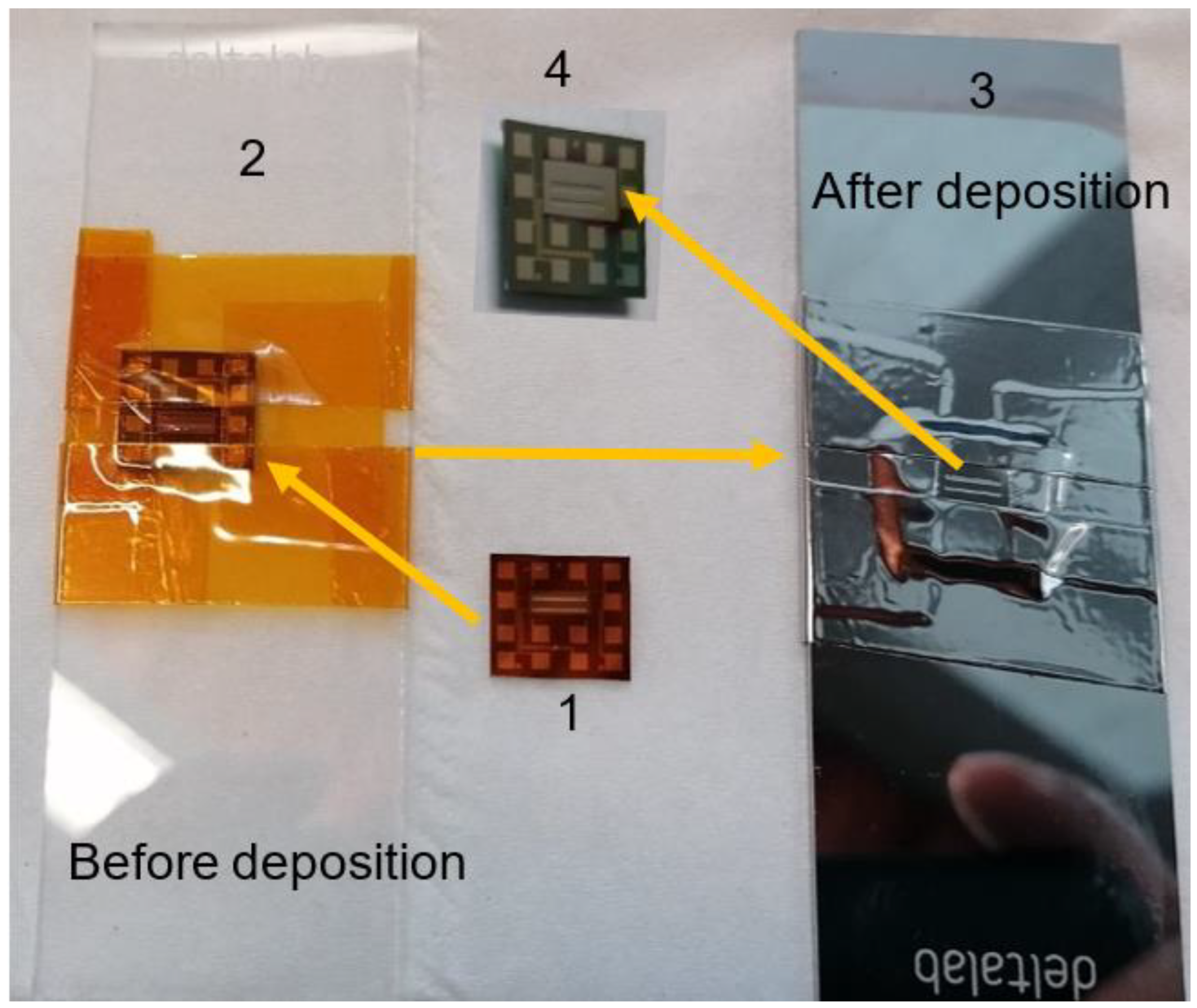
An advanced platform for the in-plane ZT measurement was used to measure the thermal electric properties of the thin film. The film was deposited on a special ZT Al2O3 (ALD) Au contact chips for Linseis TFA supplied by SemiMetrics Limited (1 in Figure 1). The chip combines two suspended membrane setups, based on the Völklein geometry for in-plane thermal conductivity measurements with a 4-point Van-der-Pauw measurement setup for the determination of the electrical transport properties [33]. The chip was first covered by a metal mask or tape, and film was deposited on specified area as shown in Figure 1. After deposition, the mask and tape were removed and the chip (4) was ready for the test. The Seebeck coefficient is measured using a partly passivated resistance thermometer, located on the bigger membrane. Electrical conductivity, Seebeck coefficient, and thermal conductivity were measured at the same time within a temperature range between −150 °C and 250 °C.
2.3. Output Mesurement of the Active Thin Layers
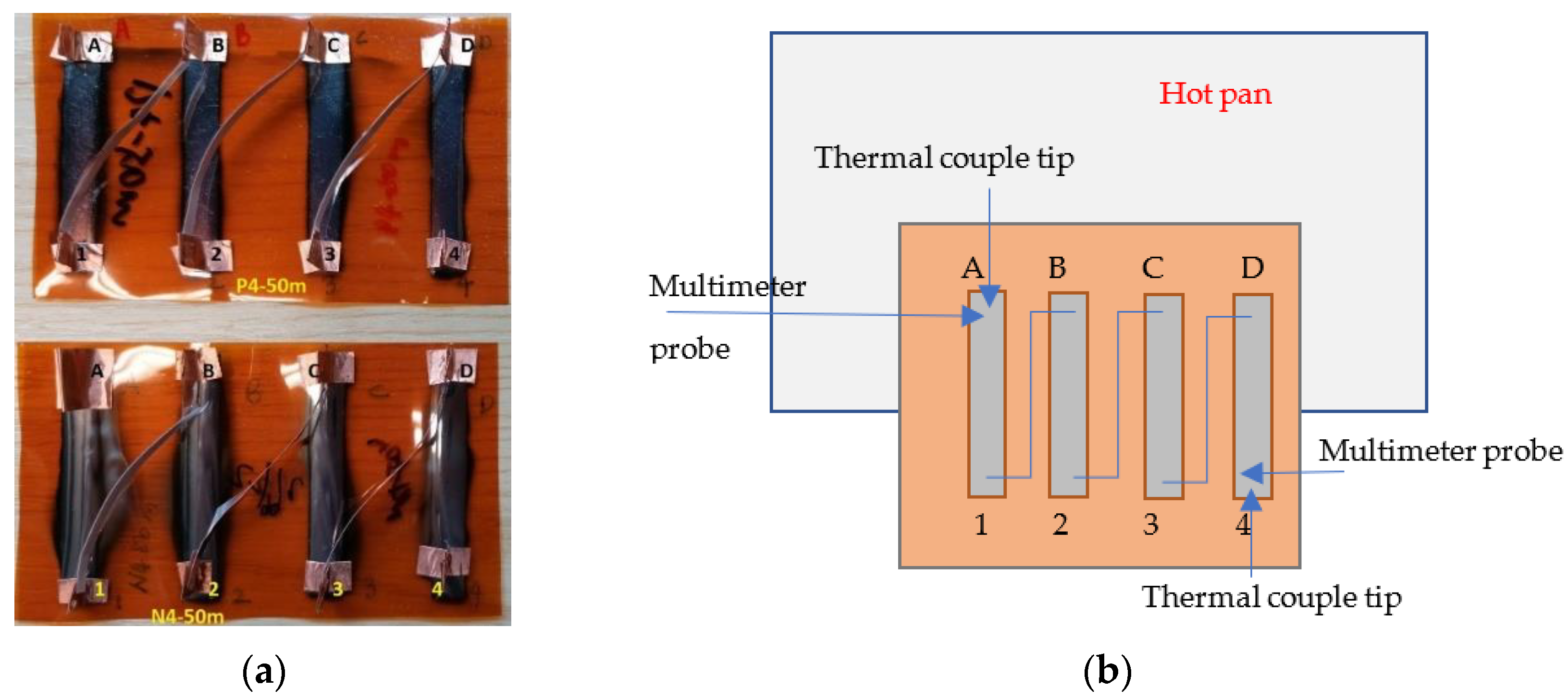
After evaluation, thin film strips with different widths and thicknesses of N-type and P-type layers were deposited on the Kapton substrate to assess their power output, as shown in Figure 2a. High-temperature conductive copper tape was used to link the strip and create connective points. One side of the strip (i.e., ABCD in Figure 2a) was put on a hot plate, which act as the heating source. The other side of the strip was left outside of the pan and cooled by naturally flowing air. Two thermal couple tips were buried under the copper tape connecting points at the hot and cold sides separately to monitor the temperature difference. One extra thermal couple tip was put on the hot pan to monitor the temperature of the heating. Two multi-meters were used to monitor the open circuit voltage/current and electrical resistance of different links such as A-1, A-4, or B-2, to assess the output of different configurations of the active layer strips. The temperature of the hot pan can be raised to 200 °C; accordingly, the tip on the active layer is about 100 °C, which can generate a temperature difference up to 80 °C. A schematic test apparatus is shown in Figure 2b.
3. Results and Discussion
3.1. Microstructure and Phase Constituents of the Thin Films
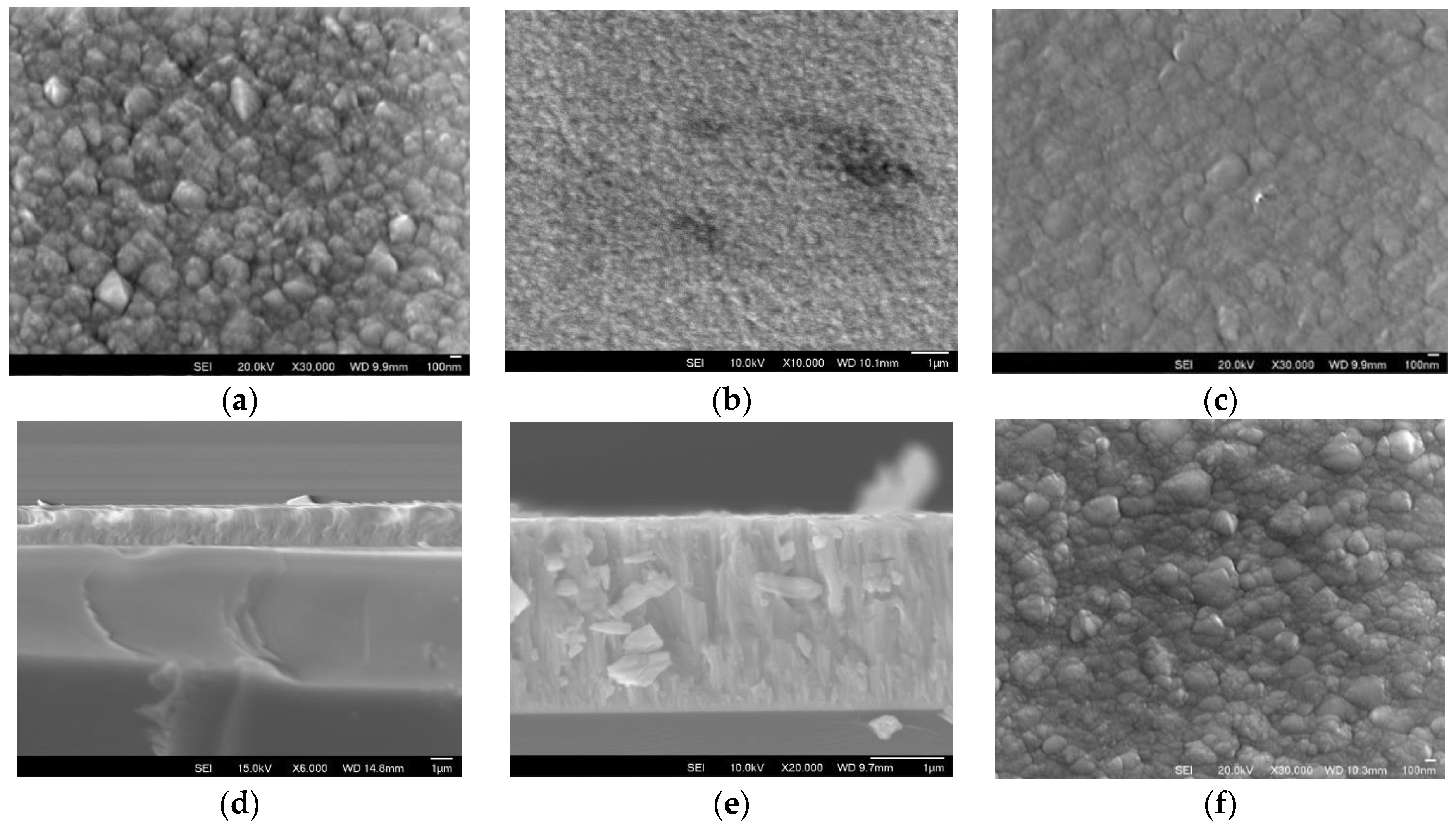
The surface morphology and cross-sectional microstructure of the P-type thin film deposited on silicon wafer with different target currents has been assessed by SEM (Figure 3). Crystallised clusters were formed on the surface after deposition, and the size only slightly changed with the increased current from 0.4 A to 0.6 A (Figure 3a–c,f). A dense fine columnar structure was formed, as seen in the cross-sectional image of P4 and P45 in Figure 3d,e. The composition of the thin film was identified by EDX, and the atomic composition ration of Bi:Sb:Te is about 2:3:4.
As shown in Table 2, both the N-type and P-type materials have a higher sputter rate, and it took only 40 min at 0.4 A to obtain a 2.0 µm thick N-type thin film. The deposition rate for P-type was slightly slower, as it took 50 min at 0.4 A to obtain only a 1.8 μm thick film. When the current was increased, the deposition was faster, but a higher current than 0.6A led to a spewing of material from the target, which adversely affected the film deposition, resulting in large particles on the surface, as evidenced in Figure 3f.
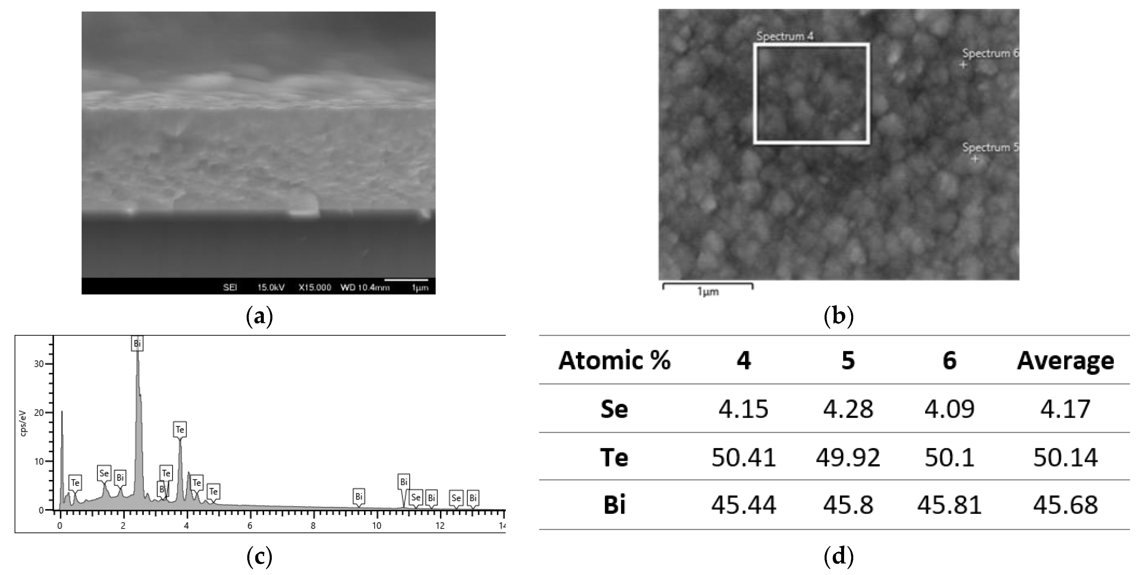
Typical cross-sectional and surface morphology images of the N-type layer on the silicon wafer are shown in Figure 4a,b. The composition of the thin film was identified by EDX, and the atomic composition was calculated as demonstrated in Figure 4c,d.
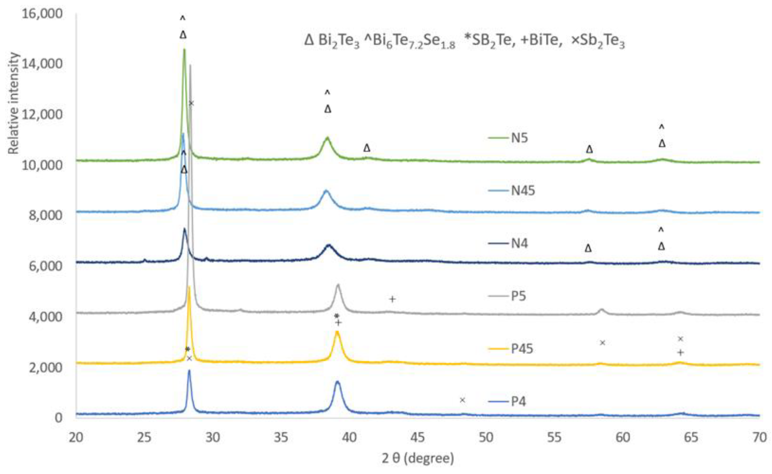
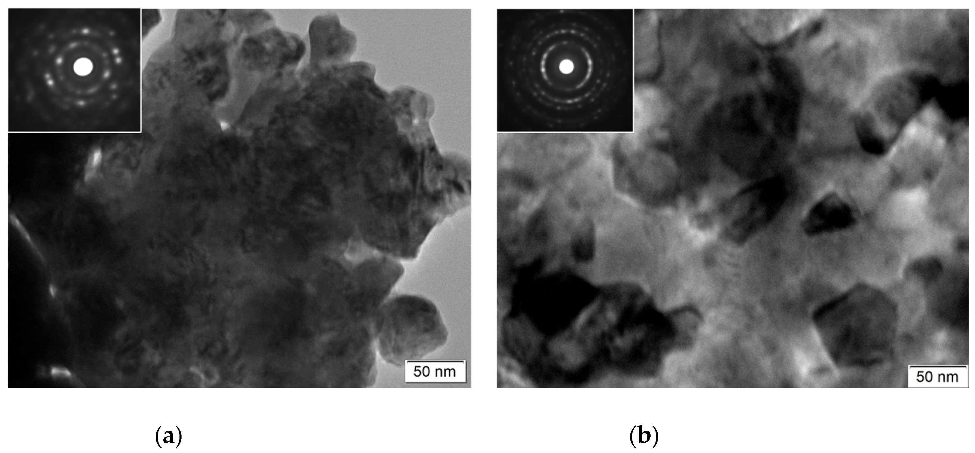
Analyzing XRD patterns taken from the N-type and P-type thin films revealed similar phase constituents for each type film, and the representatives of the patterns are shown in (Figure 5). It can be seen that the N-type thin film consists of phases of Bi2Te3 (PDF001-085-0439) and Bi6Te7.2 Se1.8 (PDF096-0151-1977), while the P-type thin film is composed of three phases: Sb2Te (PDF0001-0080-1722), BiTe (PDF0001-0089-4303, and Sb2Te3 (PDF0000-0015-0874). For the N-type thin film, the grain size (Bi2Te3 at 2θ = 27.89°) increased with the deposition current, for example, it was about 28 nm for N4 as calculated using Scherrer’s equation, while it grew to about 45 nm for N5. Similarly, for the P-type film, the crystalline size (SB2Te3 at 2θ = 28.33°) increased from about 35 nm (P4) to about 53 nm (P5). TEM observation revealed equiaxed nano-grains with dimeters of 40–70 nm, as shown in Figure 6. SAD patterns taken from both P-type and N-type thin films featured ring-patterns, characteristic of nano-structured grains. The indexing of the d-spacing values calculated from the SAD patterns confirmed the phase composition results of the XRD analysis, shown in Figure 5.
3.2. Thermoelectrical Properties of the Thin Films
Thermoelectric properties measurements of the N-type and P-type thin films within the temperature range from −150 °C to 230 °C were measured simultaneously in an advanced measurement platform.
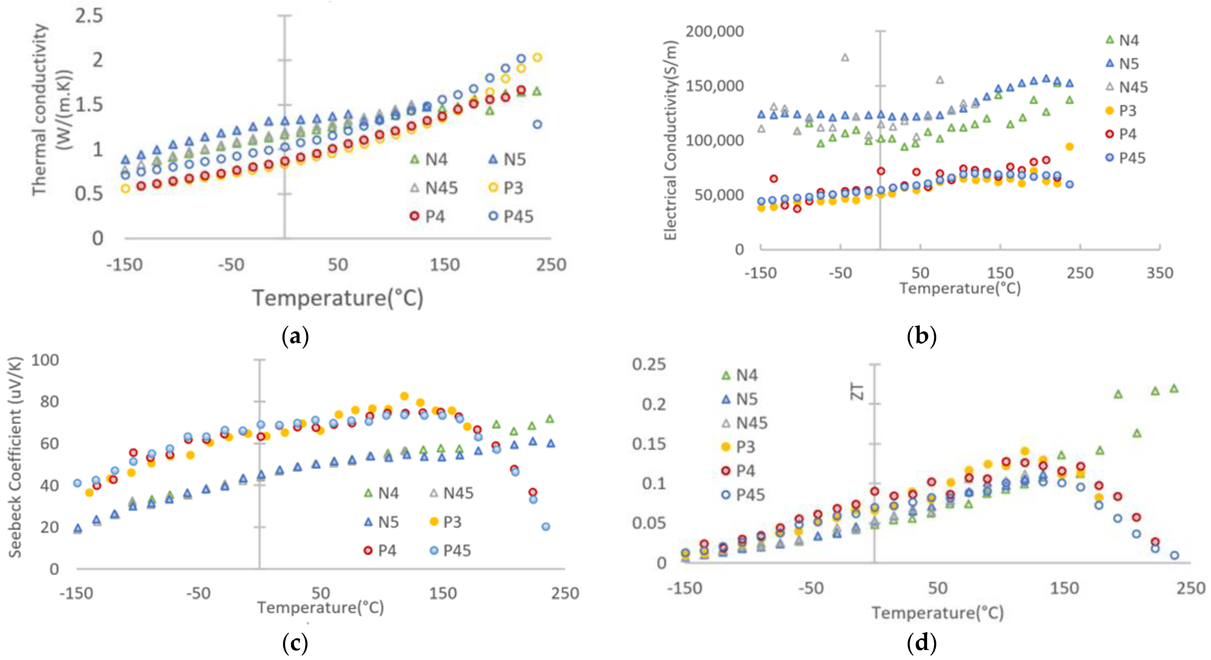
For all of the thin films, the thermal conductivity increased with the temperature, as shown in Figure 7a. Generally, the N-type layer has a higher thermal conductivity value in comparison with the P-type layer at a lower temperature range (<150 °C); this might be due to the grain-size effect as the presence of a large number of interfaces (grain boundaries), which may effectively scatter phonons while exerting a minimal effect on the transport of charge carriers [7]. In the meantime, the electrical conductivity of the N-type layers is significantly higher than those of the P-type layer, and it decreased slightly with the temperature increment from −150 °C to about 50 °C and then increased again till the end of the test (Figure 7b).
For the three P-type thin films, the electrical conductivity maintained the trend of climbing with an elevated temperature. The Seebeck coefficient of the P-type layers improved with temperature till about 140 °C and was superior to the N-type layer; however, it dropped gradually to a level lower than that of the N-type layer for further rising temperature (Figure 7c). Meanwhile, the Seebeck coefficient of N-type layers grew steadily with the temperature, which performed similarly to the N-type Bi2Te3 layer prepared at 300 C via DC magnetron sputtering [34]. As shown in Figure 7d, the calculated ZT value has a similar trend to the Seebeck coefficient, especially for the P-type layer. The ZT value change is generally higher than an 84 nm Bi87Sb13 thin film in Linseis’s work [33]. However, sample N4 performed the best at higher temperatures (>140 °C).
3.3. Output Test of the Thin Film
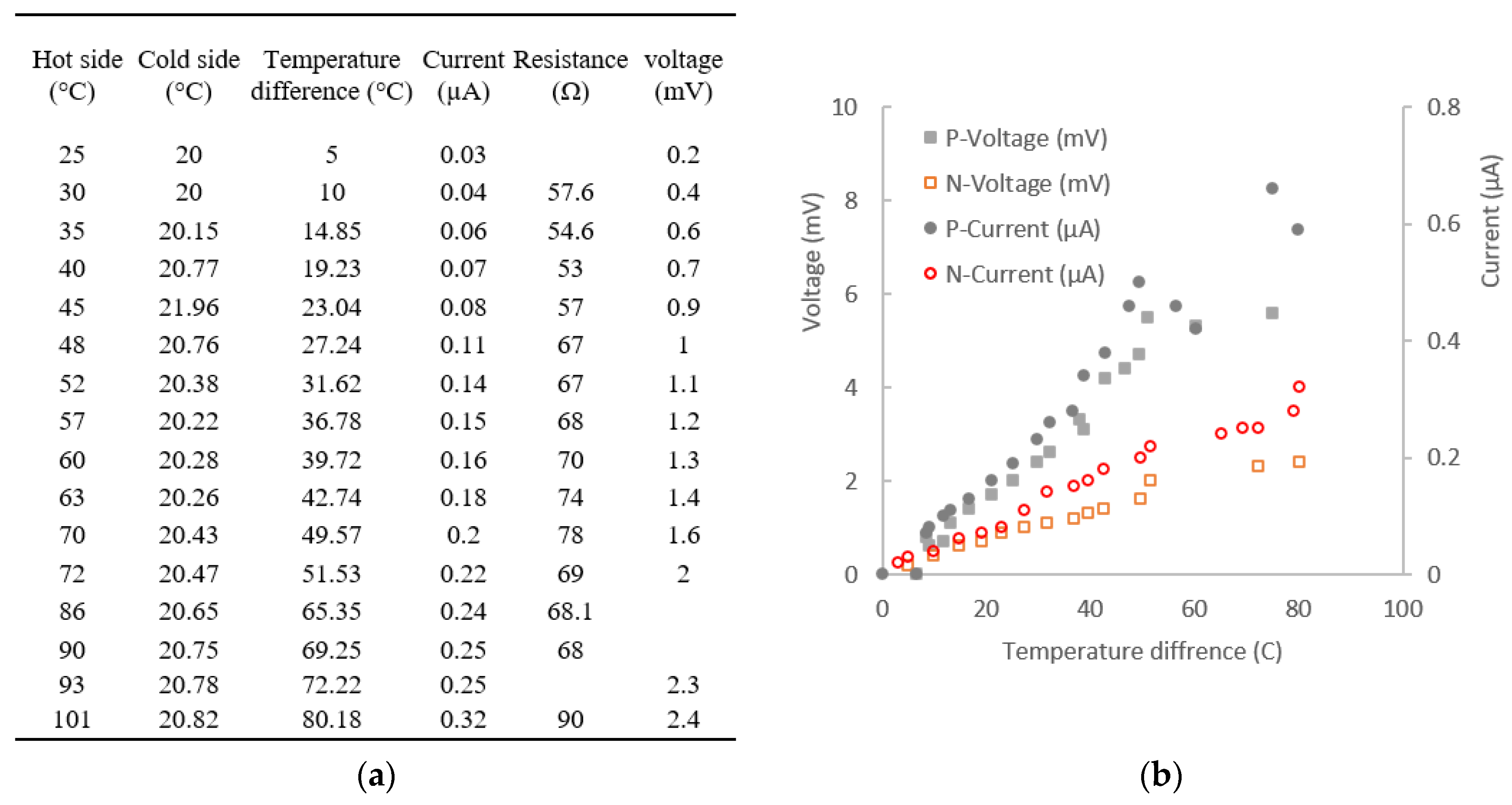
To assess the capability of the thin film in generating power, a thin film of the active layer was deposited on a glass slide of 26 × 76 mm, and the end of two sides was wrapped with copper tape to extract the energy. Part of the glass slide was put on a heating pan as a hot part, and the other side left outside the pan was cooled by air act as the cool side. When the heater was turned on, the temperature difference between the hot side and cold side produced voltage and current, which were recorded by a multi-meter, as detailed in Figure 8a. The voltage increased with the growing temperature difference, as did the electric current (Figure 8b). This is in agreement with Francioso’s finding on RF-magnetron-sputtered SB2Te3 and Bi2Te3 thin film: the open circuit voltage and electrical power increase with increasing ∆T [35]. However, they reported a maximum output at ∆T = 40 °C, and we found the open circuit voltage increased further with the difference of temperature up to 80 °C. The resistance of the thin N-type film increased slightly with the increment in temperature. A similar change was observed on the P-type thin film on glass, and the open circuit voltage and current are higher for the P-type layer than those of the N-type layer. A follow-on test of thin film on the Kapton substrate shows a similar result—that the P-type layer has a higher open-circuit voltage and current than the N-type layer.
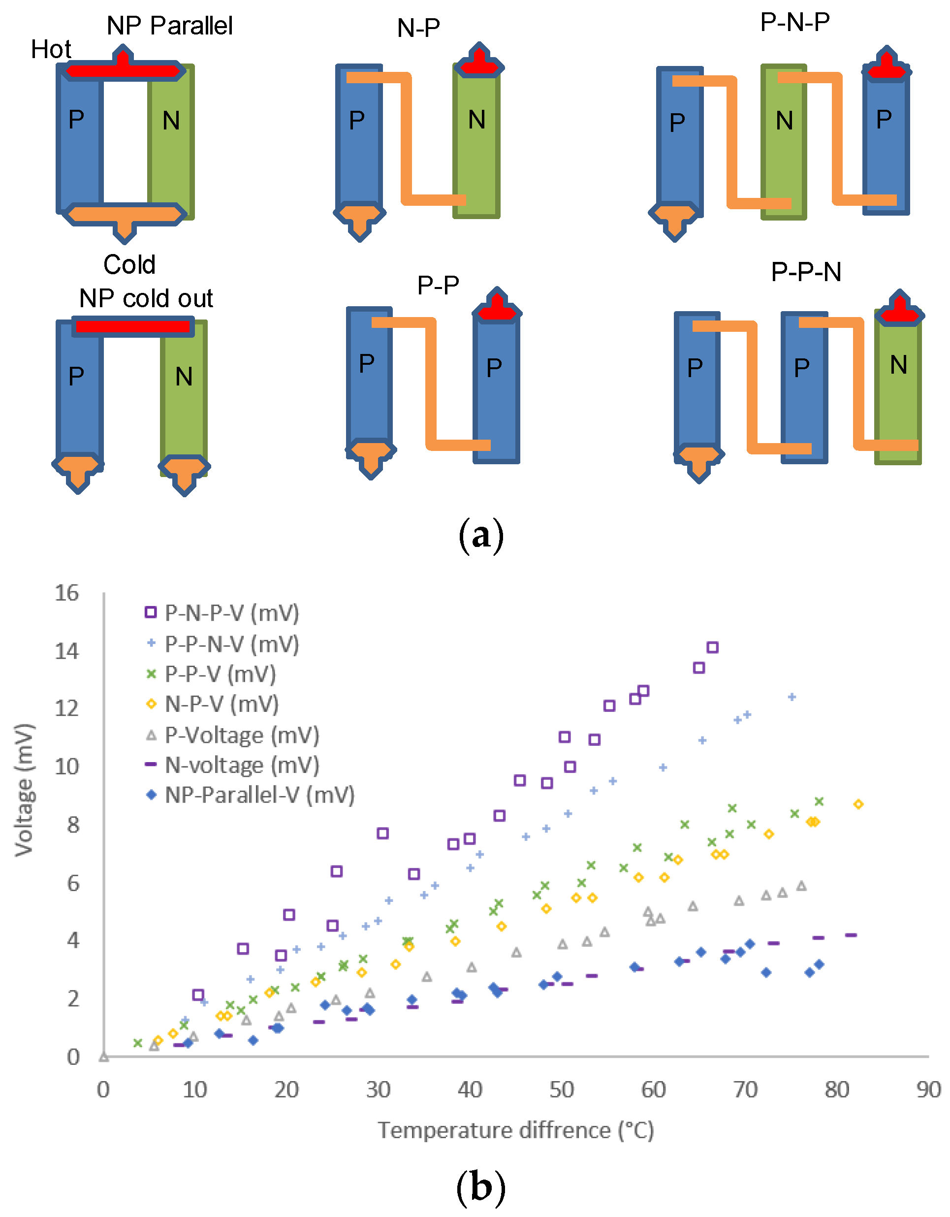
A different combination of the P-type and N-type layer (12 mm × 40 mm) on separated Kapton substrates was tested to investigate the effect of the power generation in different configurations such as P-N, P-P, N-N, PNP, PPN, etc. (Figure 9a). It was found that the hot-cold-hot-cold…series link generates most of the power; however, links such as hot side (N strip)–cold side (N strip)–cold side (P strip)–hot side (P strip) generate less power even less than one single P or N strip, as evidenced in Figure 9b.
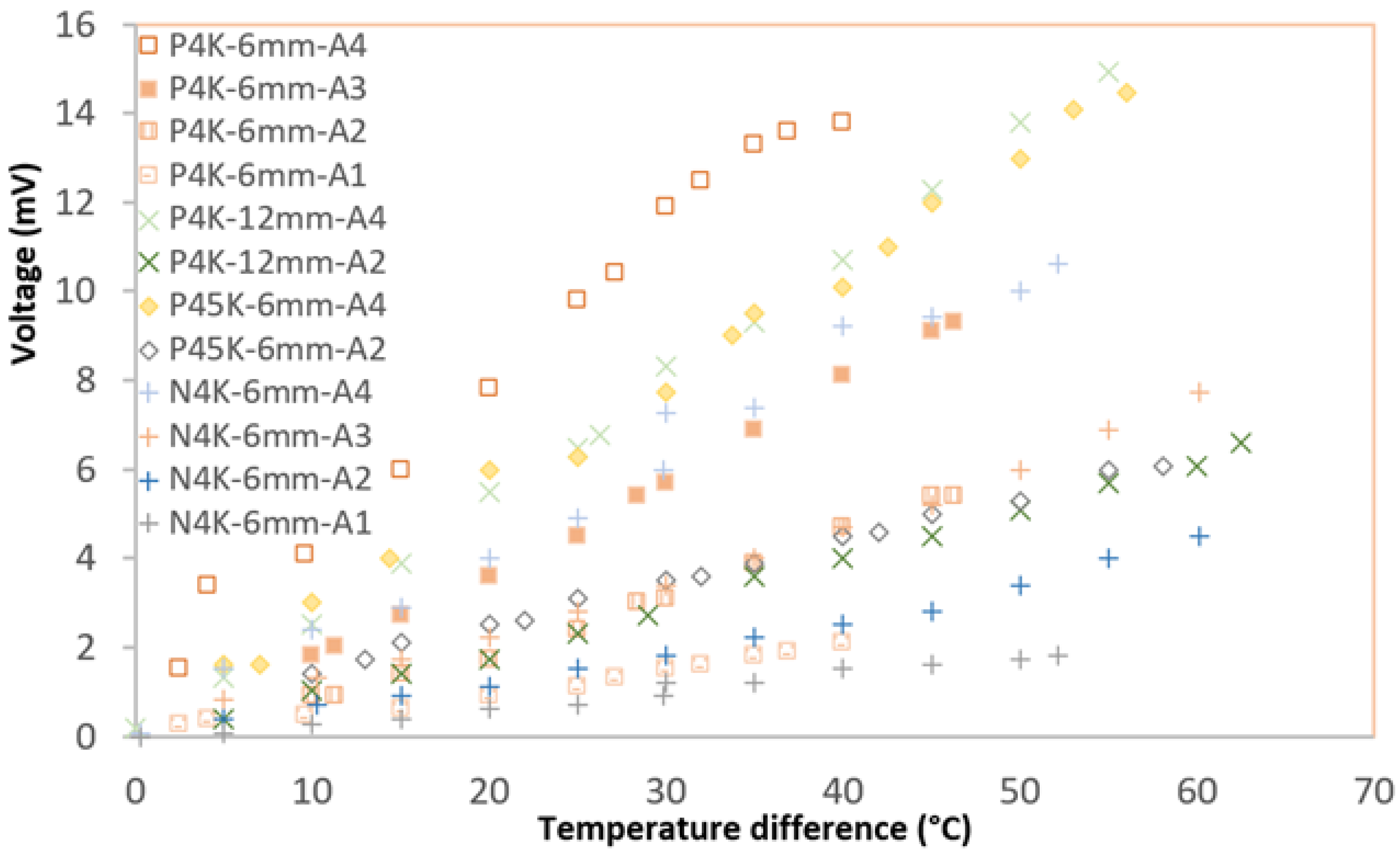
After testing different configurations of P-type and/or N-type layers, a series link of four P-type layers with different thicknesses and widths were used to assess the impact of thickness and width layer on the output of the power in the active layer (Figure 2a). Generally, when the amount of active layer was increased from one strip to four strips, the open circuit voltage increased proportionally for all of the active layers, and the same was true for the electric current output. As reported by Kwon, increasing the pair of the P-type Bi0.4Sb1.6Te3 and N-type Bi2Te3 layer grown by the metal organic vapor phase deposition can boost the power output [36]. Interestingly, the 6 mm wide and 40 mm long P-type layer (P4K-6mm) outperforms the thicker layer on Kapton for sample P45k-6 mm and a wide layer of 12 mm for P4K-12 mm in all of the strips as shown in Figure 10. In the meantime, the entire P-type layer has higher power output than the N-type layer on the Kapton substrate, i.e., N4k-6 mm.
4. Conclusions
The BiTe-based N-type and P-type thin films can be easily sputter deposited with a small target current on silicon, glass, and Kapton HN polyimide foil substrate using the DC magnetron sputtering mode. Fine columnar nano-sized grains were formed with a mixture phase of Bi2Te3 and Bi6Te7.2Se1.8 in the N-type thin film and a mixture of BiTe and Sb2Te3 in the P-type layer.
For all of the thin films, the thermal conductivity increased with the temperature. Generally, N-type layers have higher thermal conductivity and electrical conductivity in comparison with P-type layers, and both of the conductivity values have a trend of increase with elevated temperature, especially at a temperature above 0 °C. The Seebeck coefficient of P-type layers peaked at about 140 °C and was superior to that of the N-type layer, which grew steadily with temperature, while the N-type layer performed better at higher temperatures. The calculated ZT value has a similar trend to the Seebeck coefficient.
Power output tests on the different combinations of active layers suggest that a series link of active layers can maximize the output power. A series of four active layers suggests that the P-type layer has higher power output than the N-type layer on the Kapton substrate, and the longer the layer, the higher the output of current and the voltage. However, widening the strip or thickening the active layer did not improve the power output. Based on these findings, we will be able to design a device with optimized patterned thin-film strips on a flexible substrate to harvest the heat at a lower temperature range such as the photovoltaic solar cell for increasing efficiency.
Author Contributions
Conceptualization, Z.Z. and H.D.; methodology, Z.Z.; validation, Z.Z., M.G. and X.L.; formal analysis, Z.Z. and X.L.; investigation, Z.Z., H.-I.U. and M.G.; resources, Z.Z.; data curation, Z.Z.; writing—original draft preparation, Z.Z.; writing—review and editing, X.L. and H.D.; project administration, Z.Z. and H.D.; and funding acquisition, Y.Q. and H.D. All authors have read and agreed to the published version of the manuscript.
Funding
This research was funded by the EU H2020 Project ‘FAST and Nano-enabled SMART materials, Structure and System for Energy Harvesting’ (FAST-SMART) under Grant no. 862289, and supported by the Ministry of National Education of the Republic of Turkey. The Cambridge Royce facilities grant EP/P024947/1 and Sir Henry Royce Institute—recurrent grant EP/R00661X/1 are greatly appreciated.
Data Availability Statement
Not applicable.
Conflicts of Interest
The authors declare no conflict of interest.
Abbreviations
| ALD | Atomic layer deposition |
| CVD | Chemical vapor deposition |
| DC | Direct current |
| EDX | Energy dispersive X-ray spectroscopy |
| MBE | Molecular-beam epitaxy |
| MOCVD | Metalorganic chemical vapor deposition |
| PF | Power factor |
| RF | Radio frequency |
| SEM | Scanning electron microscope |
| TE | Thermoelectric |
| TPF | Thermoelectric power factor |
| TEM | Transition electron microscope |
| XRD | X-ray diffraction |
| ZT | Figure of merit |
References
- Jaldurgam, F.F.; Ahmad, Z.; Touati, F. Synthesis and Performance of Large-Scale Cost-Effective Environment-Friendly Nanostructured Thermoelectric Materials. Nanomaterials 2021, 11, 1091. [Google Scholar] [CrossRef] [PubMed]
- Liu, W.; Jie, Q.; Kim, H.S.; Ren, Z. Current progress and future challenges in thermoelectric power generation: From materials to devices. Acta Mater. 2015, 87, 357–376. [Google Scholar] [CrossRef] [Green Version]
- Ajiboye, T.O.; Onwudiwe, D.C. Bismuth sulfide based compounds: Properties, synthesis and applications. Results Chem. 2021, 3, 100151. [Google Scholar] [CrossRef]
- Yang, Z.-R.; Lin, F.-H.; Hung, P.-C.; Liu, C.-J. Type controlled thermoelectric properties in tin selenide fabricated using room-temperature synthesis and hot pressing. J. Alloys Compd. 2021, 889, 161639. [Google Scholar] [CrossRef]
- Pham, N.H.; Farahi, N.; Kamila, H.; Sankhla, A.; Ayachi, S.; Müller, E.; de Boor, J. Ni and Ag electrodes for magnesium silicide based thermoelectric generators. Mater. Today Energy 2019, 11, 97–105. [Google Scholar] [CrossRef]
- Chen, X.; Dai, W.; Wu, T.; Luo, W.; Yang, J.; Jiang, W.; Wang, L. Thin Film Thermoelectric Materials: Classification, Characterization, and Potential for Wearable Applications. Coatings 2018, 8, 244. [Google Scholar] [CrossRef] [Green Version]
- Hamawandi, B.; Mansouri, H.; Ballikaya, S.; Demirci, Y.; Orlovská, M.; Bolghanabadi, N.; Sajjadi, S.; Toprak, M. A Comparative Study on the Thermoelectric Properties of Bismuth Chalcogenide Alloys Synthesized through Mechanochemical Alloying and Microwave-Assisted Solution Synthesis Routes. Front. Mater. 2020, 7, 569723. [Google Scholar] [CrossRef]
- Tan, M.; Deng, Y.; Hao, Y. Improved thermoelectric performance of a film device induced by densely columnar Cu electrode. Energy 2014, 70, 143–148. [Google Scholar] [CrossRef]
- Peranio, N.; Winkler, M.; Bessas, D.; Aabdin, Z.; König, J.; Böttner, H.; Hermann, R.P.; Eibl, O. Room-temperature MBE deposition, thermoelectric properties, and advanced structural characterization of binary Bi2Te3 and Sb2Te3 thin films. J. Alloys Compd. 2012, 521, 163–173. [Google Scholar] [CrossRef]
- You, H.; Hyub Baek, S.; Kim, K.-C.; Kwon, O.J.; Kim, J.-S.; Park, C. Growth and thermoelectric properties of Bi2Te3 films deposited by modified MOCVD. J. Cryst. Growth 2012, 346, 17–21. [Google Scholar] [CrossRef]
- Amiri, L.; Narjis, A.; Nkhaili, L.; Bousseta, M.; Elmassi, S.; Tchenka, A.; Drissi, S.; Abali, A.; Somaily, H.H.; El Kissani, A.; et al. Spectroscopic study and thermoelectric properties of copper sulfide thin films prepared by the flash evaporation method. J. Alloys Compd. 2022, 924, 166479. [Google Scholar] [CrossRef]
- Khumtong, T.; Sukwisute, P.; Sakulkalavek, A.; Sakdanuphab, R. Microstructure and electrical properties of antimony telluride thin films deposited by RF magnetron sputtering on flexible substrate using different sputtering pressures. J. Electron. Mater. 2017, 46, 3166–3171. [Google Scholar] [CrossRef]
- Shen, S.; Zhu, W.; Deng, Y.; Zhao, H.; Peng, Y.; Wang, C. Enhancing thermoelectric properties of Sb2Te3 flexible thin film through microstructure control and crystal preferential orientation engineering. Appl. Surf. Sci. 2017, 414, 197–204. [Google Scholar] [CrossRef]
- Kim, D.-H.; Byon, E.; Lee, G.-H.; Cho, S. Effect of deposition temperature on the structural and thermoelectric properties of bismuth telluride thin films grown by co-sputtering. Thin Solid Film. 2006, 510, 148–153. [Google Scholar] [CrossRef]
- Kurokawa, T.; Mori, R.; Norimasa, O.; Chiba, T.; Eguchi, R.; Takashiri, M. Influences of substrate types and heat treatment conditions on structural and thermoelectric properties of nanocrystalline Bi2Te3 thin films formed by DC magnetron sputtering. Vacuum 2020, 179, 109535. [Google Scholar] [CrossRef]
- Jitthamapirom, P.; Wanarattikan, P.; Nuthongkum, P.; Sakdanuphab, R.; Sakulkalavek, A. Comparison of thermoelectric properties of flexible bismuth telluride thin films deposited via DC and RF magnetron sputtering. Ferroelectrics 2019, 552, 64–72. [Google Scholar] [CrossRef]
- Takayama, K.; Takashiri, M. Multi-layered-stack thermoelectric generators using p-type Sb2Te3 and n-type Bi2Te3 thin films by radio-frequency magnetron sputtering. Vacuum 2017, 144, 164–171. [Google Scholar] [CrossRef]
- Prainetr, N.; Vora-ud, A.; Thaowonkaew, S.; Horprathum, M.; Muthitamongkol, P.; Seetawan, T. Effect of substrates on thermoelectric properties of Ag–Sb–Te thin films within the temperature annealing. Phys. B Condens. 2020, 582, 411977. [Google Scholar] [CrossRef]
- Vora-ud, A.; Kumar, M.; bong Jin, S.; Muthitamongkol, P.; Horprathum, M.; Thaowonkaew, S.; Chao-moo, W.; Thanachayanont, C.; Thang, P.B.; Seetawan, T. Microstructural control by substrate heating in Pulse-DC sputtering induced thermoelectric Ge2Sb2Te5 thin films. J. Alloys Compd. 2018, 763, 430–435. [Google Scholar] [CrossRef]
- Fan, P.; Fan, W.-F.; Zheng, Z.-H.; Zhang, Y.; Luo, J.-T.; Liang, G.-X.; Zhang, D.-P. Thermoelectric properties of zinc antimonide thin film deposited on flexible polyimide substrate by RF magnetron sputtering. J. Mater. Sci. Mater. Electron. 2014, 25, 5060–5065. [Google Scholar] [CrossRef]
- Burmistrova, P.V.; Maassen, J.; Favaloro, T.; Saha, B.; Salamat, S.; Rui Koh, Y.; Lundstrom, M.S.; Shakouri, A.; Sands, T.D. Thermoelectric properties of epitaxial ScN films deposited by reactive magnetron sputtering onto MgO (001) substrates. J. Appl. Phys. 2013, 113, 153704. [Google Scholar] [CrossRef] [Green Version]
- Perez-Taborda, J.A.; Vera, L.; Caballero-Calero, O.; Lopez, E.O.; Romero, J.J.; Stroppa, D.G.; Briones, F.; Martin-Gonzalez, M. Pulsed hybrid reactive magnetron sputtering for high zT Cu2Se thermoelectric films. Adv. Mater. Technol. 2017, 2, 1700012. [Google Scholar] [CrossRef] [Green Version]
- Song, L.; Zhang, J.; Iversen, B.B. Enhanced thermoelectric properties of SnSe thin films grown by single-target magnetron sputtering. J. Mater. Chem. A 2019, 7, 17981–17986. [Google Scholar] [CrossRef]
- Chen, Z.; Shen, T.; Li, K.; Si, J. Effect of substrate temperature on structural and thermoelectric properties of RF magnetron sputtered SnSe thin film. Funct. Mater. Lett. 2019, 12, 1950040. [Google Scholar] [CrossRef]
- Tani, J.-I.; Ishikawa, H. Thermoelectric properties of Mg2Sn thin films fabricated using radio frequency magnetron sputtering. Thin Solid Film. 2019, 692, 137601. [Google Scholar] [CrossRef]
- Tani, J.-I.; Kido, H. Electrical properties of Mg2Si thin films on flexible polyimide substrates fabricated by radio-frequency magnetron sputtering. J. Ceram. Soc. Jpn. 2015, 123, 298–301. [Google Scholar] [CrossRef]
- Nowak, D.; Turkiewicz, M.; Solnica, N. Thermoelectric Properties of Thin Films of Germanium-Gold Alloy Obtained by Magnetron Sputtering. Coatings 2019, 9, 120. [Google Scholar] [CrossRef] [Green Version]
- Song, L.; Zhang, J.; Iversen, B.B. Microstructure and Thermoelectric Properties of Zn1–x Ag x Sb Thin Films Grown by Single-Target Magnetron Sputtering. ACS Appl. Energy Mater. 2020, 3, 2055–2062. [Google Scholar] [CrossRef]
- Matsuda, T.; Uenuma, M.; Kimura, M. Thermoelectric effects of amorphous Ga–Sn–O thin film. Jpn. J. Appl. Phys. 2017, 56, 070309. [Google Scholar] [CrossRef]
- Schaeuble, N.; Romanyuk, Y.; Aguirre, M.; Shkabko, A.; Yoon, S.; Weidenkaff, A. Aluminium-Substituted Zinc Oxide Thin Films: Thermoelectric Properties and Structural Characterisation. In Proceedings of the 8th European Conference on Thermoelectrics (ECT 2010), Como, Italy, 22–24 September 2010. [Google Scholar]
- Fan, P.; Zhang, Y.; Zheng, Z.-H.; Fan, W.-F.; Luo, J.-T.; Liang, G.-X.; Zhang, D.-P. Thermoelectric properties of cobalt antimony thin films deposited on flexible substrates by radio frequency magnetron sputtering. J. Electron. Mater. 2015, 44, 630–635. [Google Scholar] [CrossRef]
- Chen, R.; Lee, J.; Lee, W.; Li, D. Thermoelectrics of Nanowires. Chem. Rev. 2019, 119, 9260–9302. [Google Scholar] [CrossRef] [PubMed]
- Linseis, V.; Völklein, F.; Reith, H.; Nielsch, K.; Woias, P. Advanced platform for the in-plane ZT measurement of thin films. Rev. Sci. Instrum. 2018, 89, 015110. [Google Scholar] [CrossRef] [PubMed]
- He, Z.; Chen, Y.-X.; Zheng, Z.; Li, F.; Liang, G.; Luo, J.; Fan, P. Enhancement of thermoelectric performance of N-type Bi2Te3 based thin films via in situ annealing during magnetron sputtering. Ceram. Int. 2020, 46, 13365–13371. [Google Scholar] [CrossRef]
- Francioso, L.; De Pascali, C.; Farella, I.; Martucci, C.; Cret, P.; Siciliano, P.; Perrone, A. Flexible thermoelectric generator for ambient assisted living wearable biometric sensors. J. Power Sources 2011, 196, 3239–3243. [Google Scholar] [CrossRef]
- Kwon, S.-D.; Ju, B.-k.; Yoon, S.-J.; Kim, J.-S. Fabrication of Bismuth Telluride-Based Alloy Thin Film Thermoelectric Devices Grown by Metal Organic Chemical Vapor Deposition. J. Electron. Mater. 2009, 38, 920–924. [Google Scholar] [CrossRef]
Figure 1.
The preparation of thin film on chip: 1, the chip; 2, chip with attached shadow masks; 3, chips after deposition; and 4, chip with defined thin film ready for test.
Figure 1.
The preparation of thin film on chip: 1, the chip; 2, chip with attached shadow masks; 3, chips after deposition; and 4, chip with defined thin film ready for test.

Figure 2.
Setup for the measurement of the power output of thin film on Kapton substrate: (a) the film strips on Kapton substrate; (b) the sketch of the Kapton on a hot pan for test.
Figure 2.
Setup for the measurement of the power output of thin film on Kapton substrate: (a) the film strips on Kapton substrate; (b) the sketch of the Kapton on a hot pan for test.

Figure 3.
P-type BiSb2Te3 thin film deposited on silicon wafer: (a,d) P4, (b,e) P45, (c) P5, and (f) P6.
Figure 3.
P-type BiSb2Te3 thin film deposited on silicon wafer: (a,d) P4, (b,e) P45, (c) P5, and (f) P6.

Figure 4.
N-type (N4) Bi2Te3Se thin film deposited at 0.4A for 40 min: (a) cross-section; (b) surface; (c) EDX spectrum of Zone 4 in b; and (d) atomic composition of the film.
Figure 4.
N-type (N4) Bi2Te3Se thin film deposited at 0.4A for 40 min: (a) cross-section; (b) surface; (c) EDX spectrum of Zone 4 in b; and (d) atomic composition of the film.

Figure 5.
XRD comparison of different N-type and P-type layers on silicon substrate.

Figure 6.
TEM microstructure and corresponding SAD patterns of (a) N5 and (b) P4.

Figure 7.
Thermal electric property measurements of the N-type and P-type thin films within the temperature range −150 °C to 230 °C: (a) thermal conductivity; (b) electrical conductivity; (c) absolute value change of Seebeck coefficient; and (d) calculated ZT value.
Figure 7.
Thermal electric property measurements of the N-type and P-type thin films within the temperature range −150 °C to 230 °C: (a) thermal conductivity; (b) electrical conductivity; (c) absolute value change of Seebeck coefficient; and (d) calculated ZT value.

Figure 8.
The output of thin film for both P-type (P4-G) and N-type (N4-G) layer on glass slide: (a) detail of the temperature change and related power output and resistance change; (b) the change of open circuit voltage and current against temperature difference.
Figure 8.
The output of thin film for both P-type (P4-G) and N-type (N4-G) layer on glass slide: (a) detail of the temperature change and related power output and resistance change; (b) the change of open circuit voltage and current against temperature difference.

Figure 9.
(a) Configuration of P-type and N-type layer (12 mm × 30 mm) on Kapton substrate; (b) open-circuit voltage–output comparison.
Figure 9.
(a) Configuration of P-type and N-type layer (12 mm × 30 mm) on Kapton substrate; (b) open-circuit voltage–output comparison.

Figure 10.
Open circuit voltage output of P-type layer with different widths (P4k-6 mm and P4k-12 mm) and thicknesses (P4k:2 μm and P45k:2.5 μm) on Kapton substrate.
Figure 10.
Open circuit voltage output of P-type layer with different widths (P4k-6 mm and P4k-12 mm) and thicknesses (P4k:2 μm and P45k:2.5 μm) on Kapton substrate.


Table 1.
Thermoelectric films produced by magnetron-sputtering techniques.
| TE Film | Substrate | MS Parameters | Properties | Ref. |
|---|---|---|---|---|
| Sb2Te3 | Polyimide | RF | TPF: 1.07 × 10⁻⁴ Wm−1K−2 | [12] |
| Sb2Te3 | Polyimide | DC, deposited at 473 K | TPF: 6.0 × 10⁻⁴ Wm−1K−2 | [13] |
| Bi2Te3 | SiO2/Si | RF | TPF: 3 × 10⁻⁴Wm−1K−2 at 498 K | [14] |
| Bi2Te3 | Glass, alumina, sapphire, and polyimide | DC | S: maximum −1.63 × 10⁻⁴W/K on glass | [15] |
| Bi2Te3 | Polyimide | RF/DC | TPF: 3.5 × 10⁻³ Wm−1K−2 at 558 K with DC power | [16] |
| Sb2Te3 Bi2Te3 | Glass | RF | TPF: 1.27 × 10⁻³ Wm−1K−2 for Sb2Te3 at RT, and 1.02 × 10⁻³ Wm−1K−2 for Bi2Te3 at 573 K | [17] |
| Ag–Sb–Te (AST) | Soda-lime glass and SiO2/Si | DC | SiO2/Si wafer has better results with annealing at 773 K | [18] |
| Ge2Sb2Te5 | Soda-lime Glass (523 K–723 K) | Pulsed DC | TPF: 0.77 × 10⁻³ Wm−1K−2 at 673 K | [19] |
| ZnxSby | flexible polyimide | RF | TPF: 2.35 × 10⁻³ Wm−1K−2 | [20] |
| ScN | MgO (1123 K) | DC in Ar/N2 | TPF: 3.3 × 10⁻³ Wm−1K−2 at 800 K | [21] |
| Cu2Se | Copper (low-temperature) | Pulsed hybrid technique | TPF: 1.1 × 10⁻³ Wm−1K−2 κ = 0.8 ± 0.1 Wm−1K−1 | [22] |
| SnSe | Glass/fused silica | RF | TPF: 1.4 × 10⁻⁴ Wm−1K−2 at 575 K | [23,24] |
| Mg2Sn | Glass | RF | TPF: 8.5 × 10⁻⁴ Wm−1K−2 at 519 K | [25] |
| Mg2Si | Polyimide | RF | TPF: 3.3 × 10⁻⁵ Wm−1K−2 at 710 K | [26] |
| Ge–Au | Glass | Power of 320 W | Thermal conductivity: 1.1 Wm−1K−1 at 300 K | [27] |
| Zn1−xAgxSb | Fused silica | DC | TPF: 1.49 × 10⁻³ Wm−1K−2 at525 K | [28] |
| Amorphous Ga–Sn–O | Quartz | RF | TPF: 1.47 × 10⁻⁴ Wm−1K−2 at 397 K | [29] |
| Al-doped Zinc Oxide (AZO) | Soda-lime glass | RF | Maximum ZT value of 0.019 at 640 K | [30] |
| CoxSby | Polyimide | RF | Maximum TPF: 1.71 × 10⁻⁴ Wm−1K−2 | [31] |
DC: direct current, RF: radio frequency, TPF: thermoelectric power factor, PF: power factor, S: Seebeck coefficient, and κ: thermal conductivity.
Table 2.
Sample codes and deposition details.
| Sample Code | Substrate | Target Current (A) | Deposition Time (min) | Thickness (µm) |
|---|---|---|---|---|
| N4 | Si/Chip/Glass | 0.4 | 40 | 2.0 |
| N5 | Si/Chip/Glass | 0.5 | 40 | 2.5 |
| N45 | Si/Chip/Glass | 0.45 | 40 | 2.2 |
| P3 | Si/Glass | 0.3 | 65 | 2.0 |
| P3R | Si/Chip/Glass | 0.3 | 50 | 1.5 |
| P4 | Si/Chip/Glass | 0.4 | 50 | 1.8 |
| P45 | Si/Chip/Glass | 0.45 | 45 | 1.8 |
| P5 | Si/Glass | 0.5 | 45 | 1.9 |
| P6 | Si/Glass | 0.6 | 30 | 1.8 |
| P45K | Kapton | 0.45 | 60 | 2.5 |
| P4K-6mm | Kapton | 0.4 | 50 | 2.0 |
| P4K-12mm | Kapton | 0.4 | 50 | 2.0 |
| N4K-50m | Kapton | 0.4 | 50 | 2.4 |
N3-S, N3-G, and N3-K indicate N3 thin film on silicon, glass, and Kapton substrate separately.
Disclaimer/Publisher’s Note: The statements, opinions and data contained in all publications are solely those of the individual author(s) and contributor(s) and not of MDPI and/or the editor(s). MDPI and/or the editor(s) disclaim responsibility for any injury to people or property resulting from any ideas, methods, instructions or products referred to in the content. |
© 2023 by the authors. Licensee MDPI, Basel, Switzerland. This article is an open access article distributed under the terms and conditions of the Creative Commons Attribution (CC BY) license (https://creativecommons.org/licenses/by/4.0/).
Share and Cite
MDPI and ACS Style
Zhang, Z.; Gurtaran, M.; Li, X.; Un, H.-I.; Qin, Y.; Dong, H. Characterization of Magnetron Sputtered BiTe-Based Thermoelectric Thin Films. Nanomaterials 2023, 13, 208. https://0-doi-org.brum.beds.ac.uk/10.3390/nano13010208
AMA Style
Zhang Z, Gurtaran M, Li X, Un H-I, Qin Y, Dong H. Characterization of Magnetron Sputtered BiTe-Based Thermoelectric Thin Films. Nanomaterials. 2023; 13(1):208. https://0-doi-org.brum.beds.ac.uk/10.3390/nano13010208
Chicago/Turabian StyleZhang, Zhenxue, Mikdat Gurtaran, Xiaoying Li, Hio-Ieng Un, Yi Qin, and Hanshan Dong. 2023. "Characterization of Magnetron Sputtered BiTe-Based Thermoelectric Thin Films" Nanomaterials 13, no. 1: 208. https://0-doi-org.brum.beds.ac.uk/10.3390/nano13010208
Note that from the first issue of 2016, this journal uses article numbers instead of page numbers. See further details here.