

Fabrication of Li-Doped NiO Thin Films by Ultrasonic Spray Pyrolysis and Its Application in Light-Emitting Diodes

 and
and
Abstract
:1. Introduction
2. Materials and Methods
3. Results and Discussion
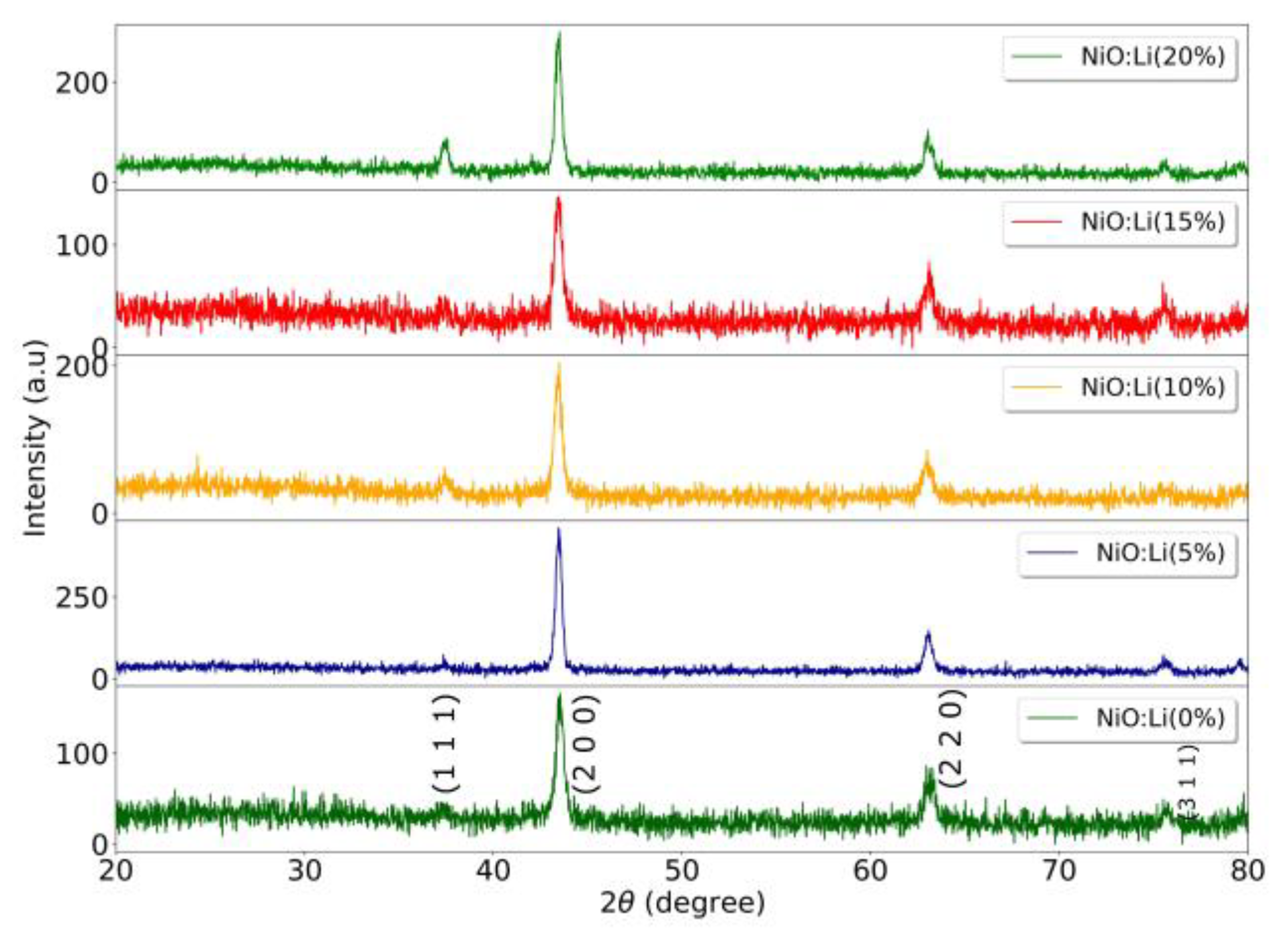
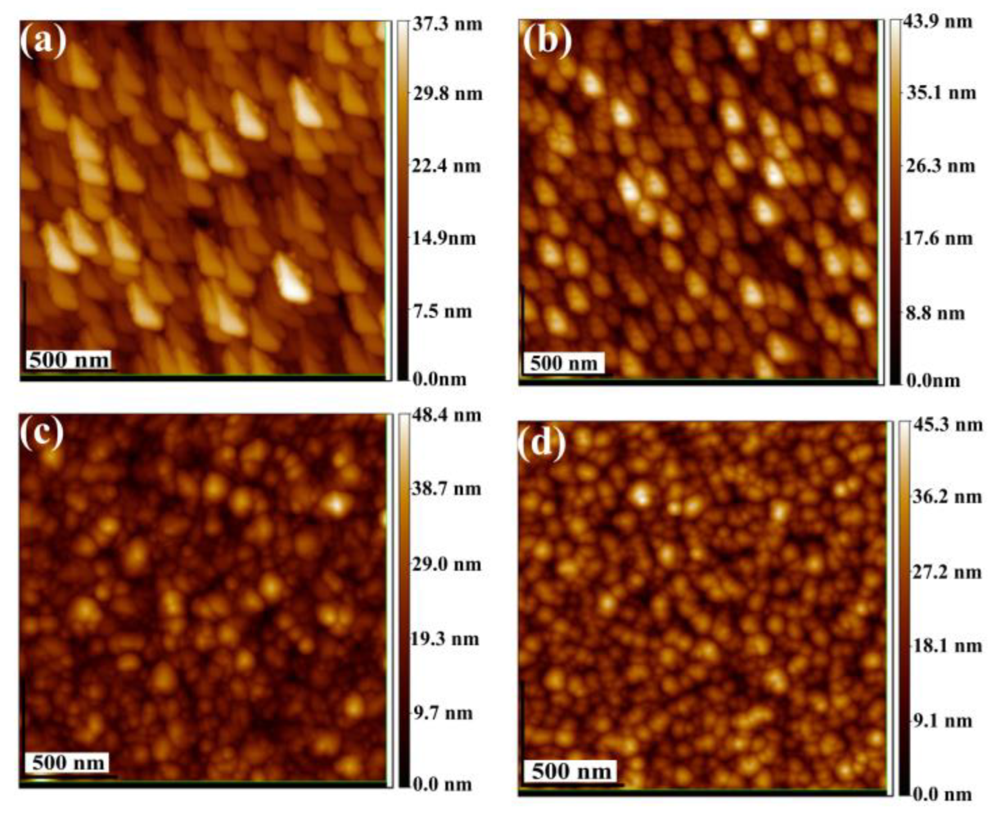
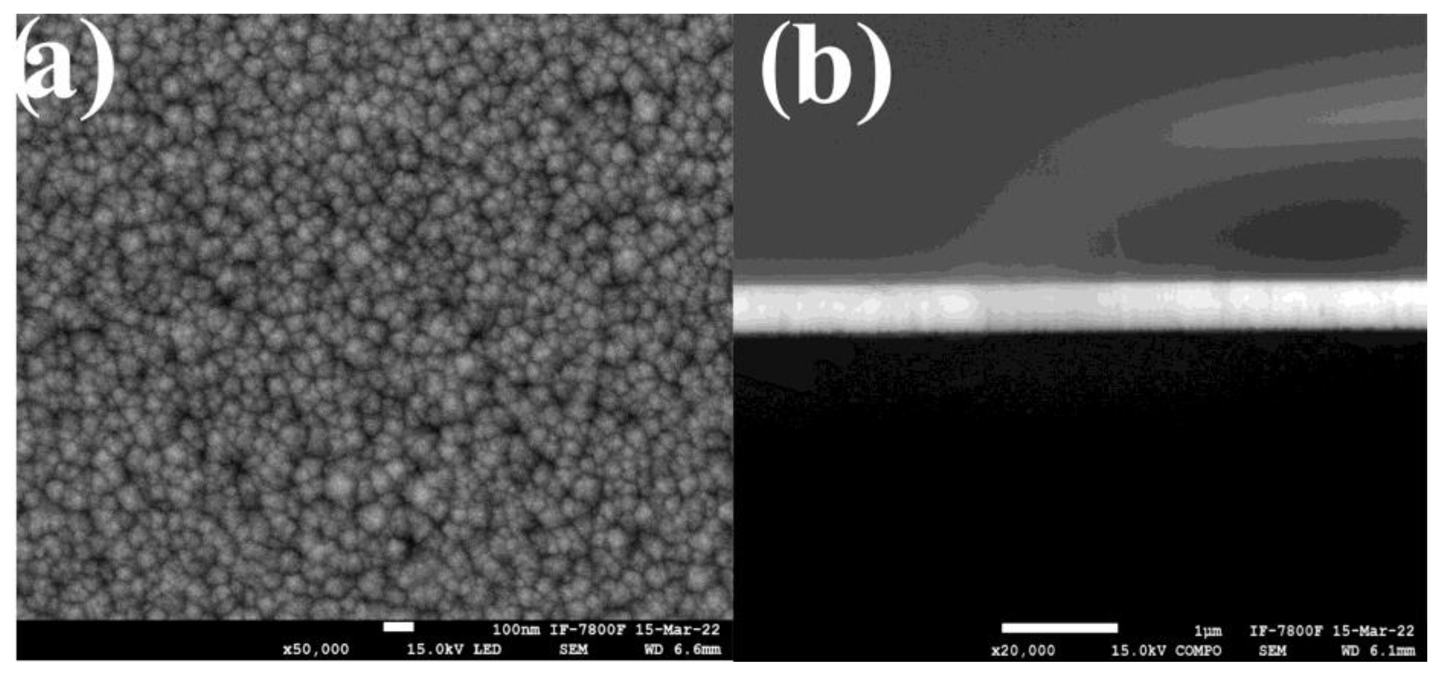
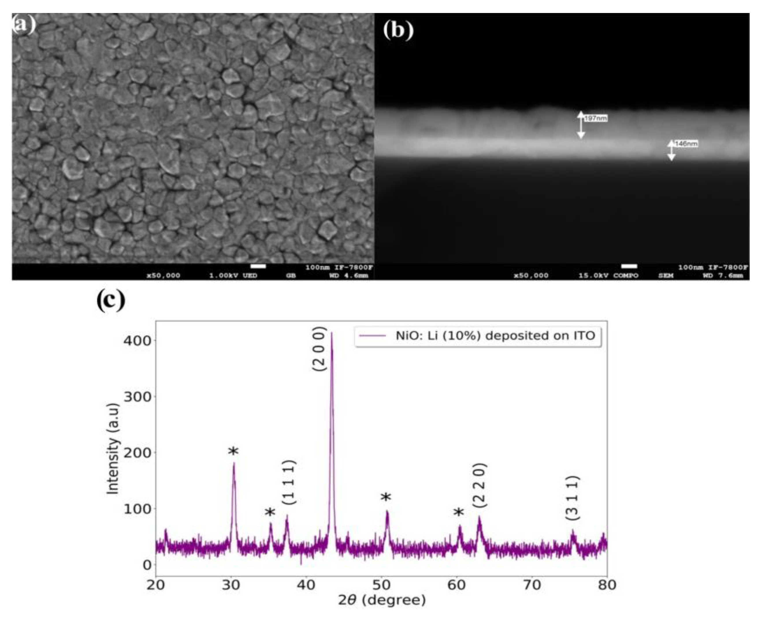
3.1. Structure and Morphology
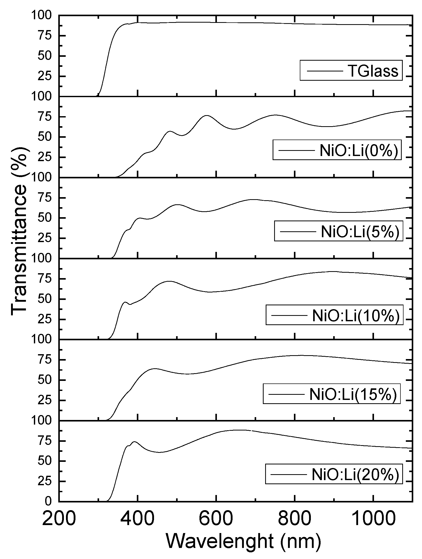
3.2. Optical and Electrical Properties
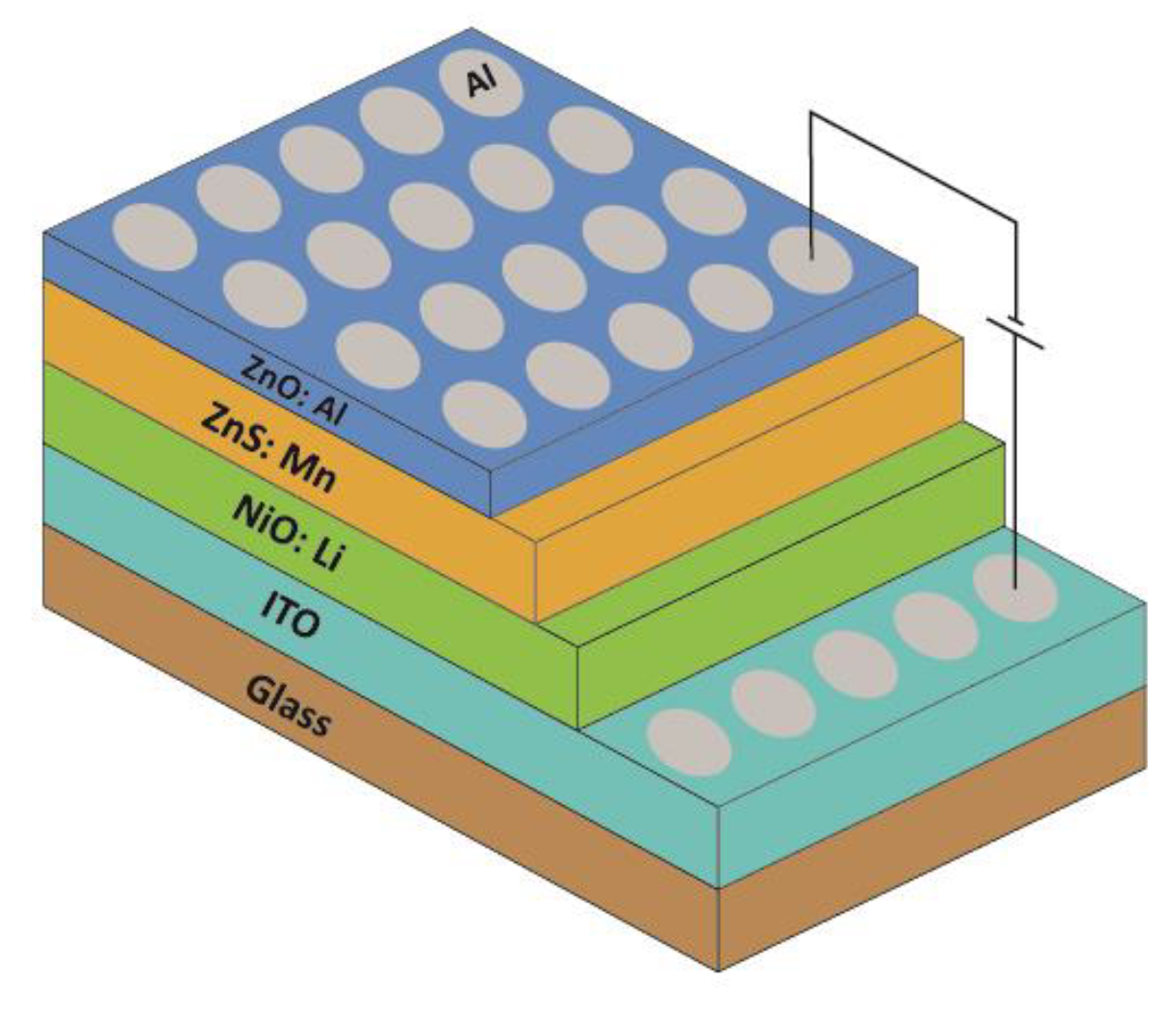
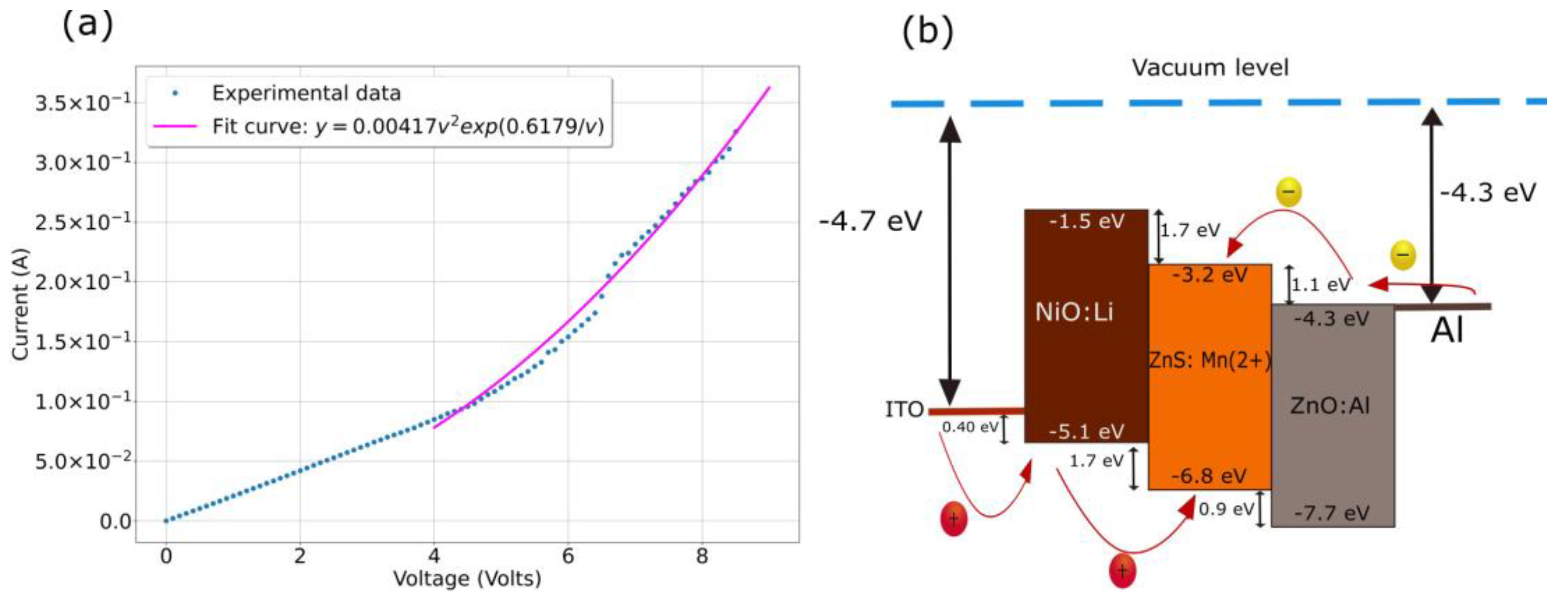
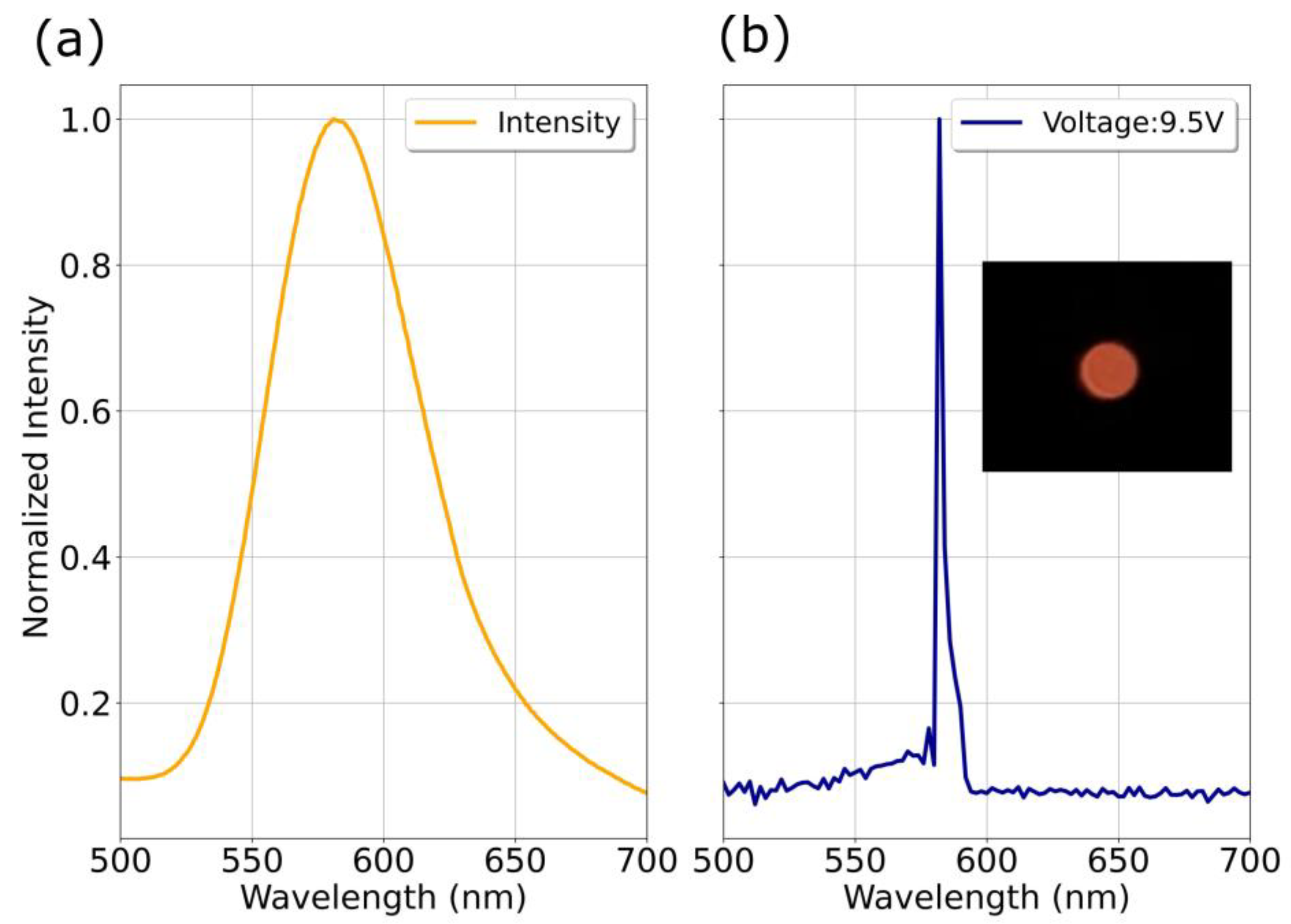
3.3. NiO: Li in a LED Structure
4. Conclusions
Author Contributions
Funding
Data Availability Statement
Acknowledgments
Conflicts of Interest
References
- Tan, G.; Tang, D.; Wang, X.; He, L.; Mu, T.; Li, G. Preparation of NiO Thin Films and Their Application for NO2 Gas Detection. Int. J. Electrochem. Sci. 2022, 17, 220551. [Google Scholar] [CrossRef]
- Gomaa, M.M.; Sayed, M.H.; Patil, V.L.; Boshta, M.; Patil, P.S. Gas Sensing Performance of Sprayed NiO Thin Films toward NO2 Gas. J. Alloys Compd. 2021, 885, 160908. [Google Scholar] [CrossRef]
- Garduño-Wilches, I.; Alonso, J.C. Hydrogen Sensors Fabricated with Sprayed NiO, NiO:Li and NiO:Li, Pt Thin Films. Int. J. Hydrogen Energy 2013, 38, 4213–4219. [Google Scholar] [CrossRef]
- Zhao, X.; Zhang, X.; Yin, Z.; Li, W.; Yang, C.; Sun, W.; Zhang, H.; Yao, L. Enhanced Electrochromic Performance of All-Solid-State Electrochromic Device Based on W-Doped NiO Films. Coatings 2022, 12, 118. [Google Scholar] [CrossRef]
- Parmar, K.H.; Manjunath, V.; Bimli, S.; Chikate, P.R.; Patil, R.A.; Ma, Y.R.; Devan, R.S. Stable and Reversible Electrochromic Behaviors in Anodic NiO Thin Films. Chinese J. Phys. 2022, 77, 143–150. [Google Scholar] [CrossRef]
- Steirer, K.X.; Chesin, J.P.; Widjonarko, N.E.; Berry, J.J.; Miedaner, A.; Ginley, D.S.; Olson, D.C. Solution Deposited NiO Thin-Films as Hole Transport Layers in Organic Photovoltaics. Org. Electron. 2010, 11, 1414–1418. [Google Scholar] [CrossRef]
- Liu, M.-H.; Zhou, Z.-J.; Zhang, P.-P.; Tian, Q.-W.; Zhou, W.-H.; Kou, D.-X.; Wu, S.-X. P-Type Li, Cu-Codoped NiOx Hole-Transporting Layer for Efficient Planar Perovskite Solar Cells. Opt. Express 2016, 24, A1349. [Google Scholar] [CrossRef]
- Islam, M.B.; Yanagida, M.; Shirai, Y.; Nabetani, Y.; Miyano, K. NiOx Hole Transport Layer for Perovskite Solar Cells with Improved Stability and Reproducibility. ACS Omega 2017, 2, 2291–2299. [Google Scholar] [CrossRef] [Green Version]
- Zhumagali, S.; Isikgor, F.H.; Maity, P.; Yin, J.; Ugur, E.; De Bastiani, M.; Subbiah, A.S.; Mirabelli, A.J.; Azmi, R.; Harrison, G.T.; et al. Linked Nickel Oxide/Perovskite Interface Passivation for High-Performance Textured Monolithic Tandem Solar Cells. Adv. Energy Mater. 2021, 11, 2101662. [Google Scholar] [CrossRef]
- Haider, M.I.; Fakhruddin, A.; Ahmed, S.; Sultan, M.; Schmidt-Mende, L. Modulating Defect Density of NiO Hole Transport Layer via Tuning Interfacial Oxygen Stoichiometry in Perovskite Solar Cells. Sol. Energy 2022, 233, 326–336. [Google Scholar] [CrossRef]
- Caruge, J.; Halpert, J.E.; Bulovic, V. NiO as an Inorganic Hole-Transporting Layer in Quantum-Dot Light-Emitting Devices. Nano Lett. 2006, 6, 2991–2994. [Google Scholar] [CrossRef] [PubMed]
- Bhaumik, S.; Pal, A.J. All-Inorganic Light-Emitting Diodes Based on Solution-Processed Nontoxic and Earth-Abundant Nanocrystals. IEEE J. Quantum Electron. 2013, 49, 325–330. [Google Scholar] [CrossRef]
- Lee, S.; Kim, D.B.; Hamilton, I.; Daboczi, M.; Nam, Y.S.; Lee, B.R.; Zhao, B.; Jang, C.H.; Friend, R.H.; Kim, J.S.; et al. Control of Interface Defects for Efficient and Stable Quasi-2D Perovskite Light-Emitting Diodes Using Nickel Oxide Hole Injection Layer. Adv. Sci. 2018, 5, 1801350. [Google Scholar] [CrossRef]
- Wang, Z.; Luo, Z.; Zhao, Z.; Guo, Q.; Wang, Y.; Wang, F.; Bian, X.; Ahmed, A.; Tasawar, H.; Tan, Z. Efficient and Stable Pure Green All-Inorganic Perovskite CsPbBr 3 Light-E Ffi Cient and Stable Pure Green All-Inorganic Perovskite CsPbBr 3 Light-Emitting Diodes with a Solution-Processed NiO x Interlayer. J. Phys. Chem. C 2017, 121, 28132–28138. [Google Scholar] [CrossRef]
- Gangishetty, M.K.; Hou, S.; Quan, Q.; Congreve, D.N. Reducing Architecture Limitations for Efficient Blue Perovskite Light-Emitting Diodes. Adv. Mater. 2018, 30, 1706226. [Google Scholar] [CrossRef]
- Wang, L.; Shi, Z.; Ma, Z.; Yang, D.; Zhang, F.; Ji, X.; Wang, M.; Chen, X.; Na, G.; Chen, S.; et al. Colloidal Synthesis of Ternary Copper Halide Nanocrystals for High- E Ffi Ciency Deep-Blue Light-Emitting Diodes with a Half-Lifetime above 100 H. Nano Lett. 2020, 20, 3568–3576. [Google Scholar] [CrossRef]
- Jeong, J.E.; Park, J.H.; Jang, C.H.; Song, M.H.; Woo, H.Y. Multifunctional Charge Transporting Materials for Perovskite Light-Emitting Diodes. Adv. Mater. 2020, 32, 2002176. [Google Scholar] [CrossRef] [PubMed]
- Wang, H.; Yuan, H.; Yu, J.; Zhang, C.; Li, K.; You, M.; Li, W.; Shao, J.; Wei, J.; Zhang, X.; et al. Boosting the Efficiency of NiOx-Based Perovskite Light-Emitting Diodes by Interface Engineering. ACS Appl. Mater. Interfaces 2020, 12, 53528–53536. [Google Scholar] [CrossRef]
- Salunkhe, P.; Muhammed, M.A.; Kekuda, D. Structural, Spectroscopic and Electrical Properties of Dc Magnetron Sputtered NiO Thin Films and an Insight into Different Defect States. Appl. Phys. A Mater. Sci. Process. 2021, 127, 390. [Google Scholar] [CrossRef]
- Nandy, S.; Saha, B.; Mitra, M.K. Effect of Oxygen Partial Pressure on the Electrical and Optical Properties of Highly (200) Oriented p-Type Ni1−xO Films by DC Sputtering Effect of Oxygen Partial Pressure on the Electrical and Optical Properties of Highly (200) Oriented p-Type Ni 1. J. Mater. Sci. 2007, 42, 5766–5772. [Google Scholar] [CrossRef]
- Sahu, D.R.; Wu, T.J.; Wang, S.C.; Huang, J.L. Electrochromic Behavior of NiO Film Prepared by E-Beam Evaporation. J. Sci. Adv. Mater. Devices 2017, 2, 225–232. [Google Scholar] [CrossRef]
- Hameed, M.A.; Ali, O.A.; Al-Awadi, S.S.M. Optical Properties of Ag-Doped Nickel Oxide Thin Films Prepared by Pulsed-Laser Deposition Technique. Optik (Stuttg) 2020, 206, 164352. [Google Scholar] [CrossRef]
- Franta, D.; Negulescu, B.; Thomas, L.; Richard, P.; Mistrı, J.; Guyot, M.; Ohlı, I. Optical Properties of NiO Thin Films Prepared by Pulsed Laser Deposition Technique. Appl. Surf. Sci. 2005, 244, 426–430. [Google Scholar] [CrossRef]
- Raza, M.H.; Movlaee, K.; Wu, Y.; El-Refaei, S.M.; Karg, M.; Leonardi, S.G.; Neri, G.; Pinna, N. Tuning the NiO Thin Film Morphology on Carbon Nanotubes by Atomic Layer Deposition for Enzyme-Free Glucose Sensing. ChemElectroChem 2019, 6, 383–392. [Google Scholar] [CrossRef]
- Kondrateva, A.S.; Mishin, M.V.; Alexandrov, S.E. TOF MS Investigation of Nickel Oxide CVD. J. Am. Soc. Mass Spectrom. 2017, 28, 2352–2360. [Google Scholar] [CrossRef]
- Yu, J.H.; Nam, S.H.; Gil, Y.E.; Boo, J.H. The Effect of Ammonia Concentration on the Microstructure and Electrochemical Properties of NiO Nanoflakes Array Prepared by Chemical Bath Deposition. Appl. Surf. Sci. 2020, 532, 147441. [Google Scholar] [CrossRef]
- Abdelghani, L.; Said, L.; Said, B.; Okba, B. Spin Coating Method Deposited Nickel Oxide Thin Films with Various Film Thicknesses. J. Chem. Res. 2022, 46, 17475198211066535. [Google Scholar] [CrossRef]
- Ivanova, T.; Harizanova, A.; Shipochka, M.; Vitanov, P. Nickel Oxide Films Deposited by Sol-Gel Method: Effect of Annealing Temperature on Structural, Optical, and Electrical Properties. Materials 2022, 15, 1742. [Google Scholar] [CrossRef]
- Akaltun, Y.; Çayır, T. Fabrication and Characterization of NiO Thin Films Prepared by SILAR Method. J. Alloys Compd. 2015, 625, 144–148. [Google Scholar] [CrossRef]
- Ukoba, K.O.; Eloka-Eboka, A.C.; Inambao, F.L. Review of Nanostructured NiO Thin Film Deposition Using the Spray Pyrolysis Technique. Renew. Sustain. Energy Rev. 2018, 82, 2900–2915. [Google Scholar] [CrossRef]
- Sharma, R.; Acharya, A.D.; Shrivastava, S.B.; Shripathi, T.; Ganesan, V. Optik Preparation and Characterization of Transparent NiO Thin Films Deposited by Spray Pyrolysis Technique. Opt.—Int. J. Light Electron Opt. 2014, 125, 6751–6756. [Google Scholar] [CrossRef]
- Rahemi Ardekani, S.; Sabour Rouh Aghdam, A.; Nazari, M.; Bayat, A.; Yazdani, E.; Saievar-Iranizad, E. A Comprehensive Review on Ultrasonic Spray Pyrolysis Technique: Mechanism, Main Parameters and Applications in Condensed Matter. J. Anal. Appl. Pyrolysis 2019, 141, 104631. [Google Scholar] [CrossRef]
- Ohta, H.; Kamiya, M.; Kamiya, T.; Hirano, M.; Hosono, H. UV-Detector Based on Pn-Heterojunction Diode Composed of Transparent Oxide Semiconductors, p-NiO/n-ZnO. Thin Solid Films 2003, 445, 317–321. [Google Scholar] [CrossRef]
- Dutta, T.; Gupta, P.; Gupta, A.; Narayan, J. Effect of Li Doping in NiO Thin Films on Its Transparent and Conducting Properties and Its Application in Heteroepitaxial P-n Junctions. J. Appl. Phys. 2010, 083715, 083715. [Google Scholar] [CrossRef]
- Zhang, J.Y.; Li, W.W.; Hoye, R.L.Z.; Macmanus-driscoll, J.L.; Budde, M. Electronic and Transport Properties of Li-Doped NiO Epitaxial Thin Films. J. Mater. Chem. C 2018, 6, 2275–2282. [Google Scholar] [CrossRef]
- Arunodaya, J.; Sahoo, T. Effect of Li Doping on Conductivity and Band Gap of Nickel Oxide Thin Film Deposited by Spin Coating Technique. Mater. Res. Express 2019, 7, 016405. [Google Scholar] [CrossRef]
- Azimi Juybari, H.; Bagheri-mohagheghi, M.; Shokooh-saremi, M. Nickel—Lithium Oxide Alloy Transparent Conducting Films Deposited by Spray Pyrolysis Technique. J. Alloys Compd. 2011, 509, 2770–2775. [Google Scholar] [CrossRef]
- Chia-Ching, W.; Cheng-Fu, Y. Investigation of the Properties of Nanostructured Li-Doped NiO Films Using the Modified Spray Pyrolysis Method. Nanoscale Res. Lett. 2013, 8, 33. [Google Scholar] [CrossRef] [Green Version]
- Yang, C.F.; Wu, C.C. Effect of Annealing Temperature on the Characteristics of the Modified Spray Deposited Li-Doped NiO Films and Their Applications in Transparent Heterojunction Diode. Sol. Energy Mater. Sol. Cells 2015, 132, 492–498. [Google Scholar] [CrossRef]
- Dawood, M.O.; Chiad, S.S.; Ghazai, A.J.; Habubi, N.F.; Abdulmunem, O.M. Effect of Li Doping on Structure and Optical Properties of NiO Nano Thin-Films by SPT. AIP Conf. Proc. 2020, 2213, 020102. [Google Scholar] [CrossRef]
- Falcony, C.; Aguilar-Frutis, M.A.; García-Hipólito, M. Spray Pyrolysis Technique; High-K Dielectric Films and Luminescent Materials: A Review. Micromachines 2018, 9, 414. [Google Scholar] [CrossRef] [PubMed] [Green Version]
- Jung, K.Y.; Kang, Y.C.; Park, Y.K. DMF Effect on the Morphology and the Luminescence Properties of Y2O3:Eu3+ Red Phosphor Prepared by Spray Pyrolysis. J. Ind. Eng. Chem. 2008, 14, 224–229. [Google Scholar] [CrossRef]
- Menaka, S.M.; Umadevi, G. Concentration Dependent Structural, Morphological, Spectral, Optical and Electrical Properties of Spray Pyrolyzed NiO Thin Films. Silicon 2018, 10, 2023–2029. [Google Scholar] [CrossRef]
- Rivera, M.J.; Ramírez, E.B.; Juárez, B.; González, J.; García-León, J.M.; Escobar-Alarcón, L.; Alonso, J.C. Low Temperature-Pyrosol-Deposition of Aluminum-Doped Zinc Oxide Thin Films for Transparent Conducting Contacts. Thin Solid Films 2016, 605, 108–115. [Google Scholar] [CrossRef]
- Shannon, R.D. Revised effective ionic radii and systematic studies of interatomic distances in halides and chalcogenides. Acta Cryst. A 1976, 32, 751–767. [Google Scholar] [CrossRef]
- Sta, I.; Jlassi, M.; Hajji, M.; Ezzaouia, H. Structural, Optical and Electrical Properties of Undoped and Li-Doped NiO Thin Films Prepared by Sol-Gel Spin Coating Method. Thin Solid Films 2014, 555, 131–137. [Google Scholar] [CrossRef]
- Iida, Y.; Hayashi, N. A Note on the Solid Chemisty of the NiO-Li 2 O Solid Solution. Bull. Chem. Soc. Jpn. 1964, 37, 659–662. [Google Scholar] [CrossRef] [Green Version]
- Garduño, I.A.; Alonso, J.; Bizarro, M.; Ortega, R.; Rodríguez-Fernández, L.; Ortiz, A. Optical and Electrical Properties of Lithium Doped Nickel Oxide Films Deposited by Spray Pyrolysis onto Alumina Substrates. J. Cryst. Growth 2010, 312, 3276–3281. [Google Scholar] [CrossRef]
- Swanepoel, R. Determination of the Thickness and Optical Constants of Amorphous Silicon. J. Phys. E Sci. Instrum. 1983, 16, 1214–1222. [Google Scholar] [CrossRef] [Green Version]
- Márquez, E.; Ruíz-Pérez, J.J.; Ballester, M.; Márquez, A.P.; Blanco, E.; Minkov, D.; Fernández Ruano, S.M.; Saugar, E. Optical Characterization of H-Free a-Si Layers Grown by Rf-Magnetron Sputtering by Inverse Synthesis Using Matlab: Tauc–Lorentz–Urbach Parameterization. Coatings 2021, 11, 1324. [Google Scholar] [CrossRef]
- Juárez-García, B.; González-Gutiérrez, J.; Rivera-Medina, M.J.; García-Valenzuela, A.; Alonso-Huitrón, J.C. Requirements and Applications of Accurate Modeling of the Optical Transmission of Transparent Conducting Coatings. Appl. Opt. 2019, 58, 5179. [Google Scholar] [CrossRef] [PubMed]
- Chakrabarty, D.K.; Raju, V.B. Solid State Properties of Lithium Doped Nickel Oxide and Its Catalytic Activity towards Dehydrogenation of Isopropanol. Proc. Indian Acad. Sci.—Sect. A Chem. Sci. 1978, 87, 133–139. [Google Scholar] [CrossRef]
- Matsubara, K.; Huang, S.; Iwamoto, M.; Pan, W. Enhanced Conductivity and Gating Effect of P-Type Li-Doped NiO Nanowires. Nanoscale 2014, 6, 688–692. [Google Scholar] [CrossRef] [PubMed]
- Huang, H.; Fang, G.; Mo, X.; Long, H.; Wang, H.; Li, S.; Li, Y.; Zhang, Y.; Pan, C.; Carroll, D.L. Improved and Orange Emission from an N-ZnO/p-Si Heterojunction Light Emitting Device with NiO as the Intermediate Layer. Appl. Phys. Lett. 2012, 101, 223504. [Google Scholar] [CrossRef]
- Fang, X.; Bando, Y.; Gautam, U.K.; Ye, C.; Golberg, D. Inorganic Semiconductor Nanostructures and Their Field-Emission Applications. J. Mater. Chem. 2008, 18, 509–522. [Google Scholar] [CrossRef]
- Ramírez, E.B.; Bizarro, M.; Alonso, J.C. Synthesis and Characterization of Thin Film Electroluminescent Devices All-Prepared by Ultrasonic Spray Pyrolysis. Thin Solid Films 2013, 548, 255–258. [Google Scholar] [CrossRef]
- Kang, T.W.; Park, K.W.; Deressa, G.; Kim, J.S. Drastic Enhancement of Blue-to-Orange Color Conversion Efficiency in Heavily-Doped ZnS:Mn2+ Phosphor and Its Application in White LEDs. J. Lumin. 2018, 194, 551–556. [Google Scholar] [CrossRef]
- Jung, B.O.; Kwon, Y.H.; Seo, D.J.; Lee, D.S.; Cho, H.K. Ultraviolet Light Emitting Diode Based on P-NiO/n-ZnO Nanowire Heterojunction. J. Cryst. Growth 2013, 370, 314–318. [Google Scholar] [CrossRef]


| Film | Grain Size (nm) | |||
|---|---|---|---|---|
| NiO (20%) | 43.446 | 2.081 | 24.3 | 4.162 |
| NiO (15%) | 43.450 | 2.081 | 21.7 | 4.162 |
| NiO (10%) | 43.442 | 2.081 | 22.6 | 4.163 |
| NiO (5%) | 43.475 | 2.080 | 25.2 | 4.160 |
| NiO (0%) | 43.540 | 2.077 | 22.1 | 4.1538 |
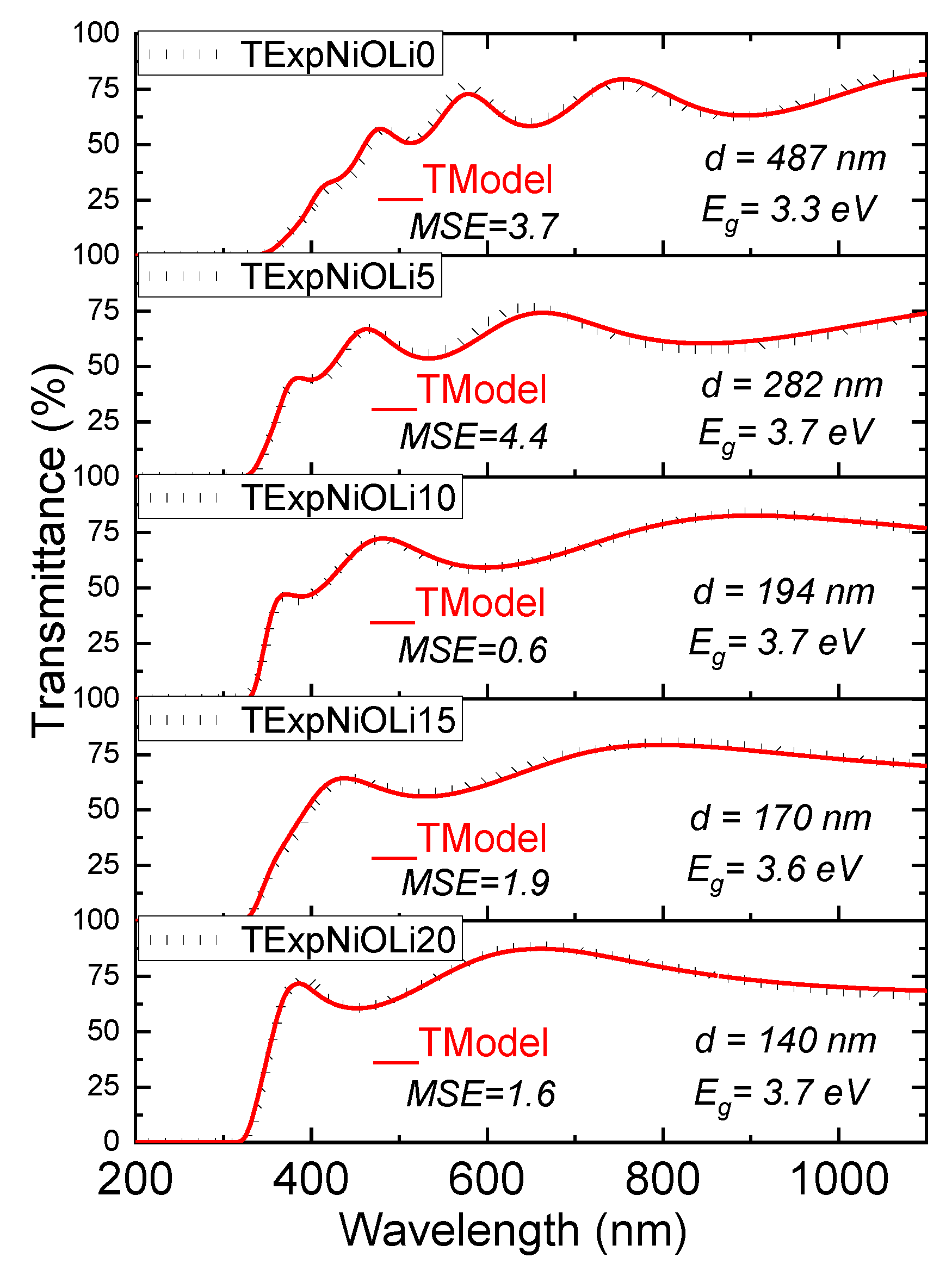
| Film | Average Transmittance (%) | Thickness (nm) | Eg(eV) |
|---|---|---|---|
| NiO:Li (20%) | 77.6 | 140 | 3.7 |
| NiO:Li (15%) | 67.1 | 170 | 3.6 |
| NiO:Li (10%) | 65.4 | 194 | 3.7 |
| NiO:Li (5%) | 63.8 | 282 | 3.7 |
| NiO:Li (0%) | 60.9 | 487 | 3.3 |
| Film | ρ (Resistivity) [Ohm—cm] | ||
|---|---|---|---|
| NiO: Li (0%) | --------------- | ------------------- | -------------------- |
| NiO: Li (5%) | 2.5 × 10³ | 3.3 × 10¹⁴ | 1.6 |
| NiO: Li (10%) | 4.4 × 10² | 4.9 × 10¹⁵ | 2.9 |
| NiO: Li (15%) | 2.8 × 10² | 2.1 × 10¹⁸ | 1.1 |
| NiO: Li (20%) | 2.3 × 10² | 1.4 × 10¹⁷ | 0.2 |
Disclaimer/Publisher’s Note: The statements, opinions and data contained in all publications are solely those of the individual author(s) and contributor(s) and not of MDPI and/or the editor(s). MDPI and/or the editor(s) disclaim responsibility for any injury to people or property resulting from any ideas, methods, instructions or products referred to in the content. |
© 2023 by the authors. Licensee MDPI, Basel, Switzerland. This article is an open access article distributed under the terms and conditions of the Creative Commons Attribution (CC BY) license (https://creativecommons.org/licenses/by/4.0/).
Share and Cite
López-Lugo, V.H.; García-Hipólito, M.; Rodríguez-Gómez, A.; Alonso-Huitrón, J.C. Fabrication of Li-Doped NiO Thin Films by Ultrasonic Spray Pyrolysis and Its Application in Light-Emitting Diodes. Nanomaterials 2023, 13, 197. https://0-doi-org.brum.beds.ac.uk/10.3390/nano13010197
López-Lugo VH, García-Hipólito M, Rodríguez-Gómez A, Alonso-Huitrón JC. Fabrication of Li-Doped NiO Thin Films by Ultrasonic Spray Pyrolysis and Its Application in Light-Emitting Diodes. Nanomaterials. 2023; 13(1):197. https://0-doi-org.brum.beds.ac.uk/10.3390/nano13010197
Chicago/Turabian StyleLópez-Lugo, Víctor Hugo, Manuel García-Hipólito, Arturo Rodríguez-Gómez, and Juan Carlos Alonso-Huitrón. 2023. "Fabrication of Li-Doped NiO Thin Films by Ultrasonic Spray Pyrolysis and Its Application in Light-Emitting Diodes" Nanomaterials 13, no. 1: 197. https://0-doi-org.brum.beds.ac.uk/10.3390/nano13010197