

Laser Ablation of Silicon Nanoparticles and Their Use in Charge-Coupled Devices for UV Light Sensing via Wavelength-Shifting Properties
 , , , and
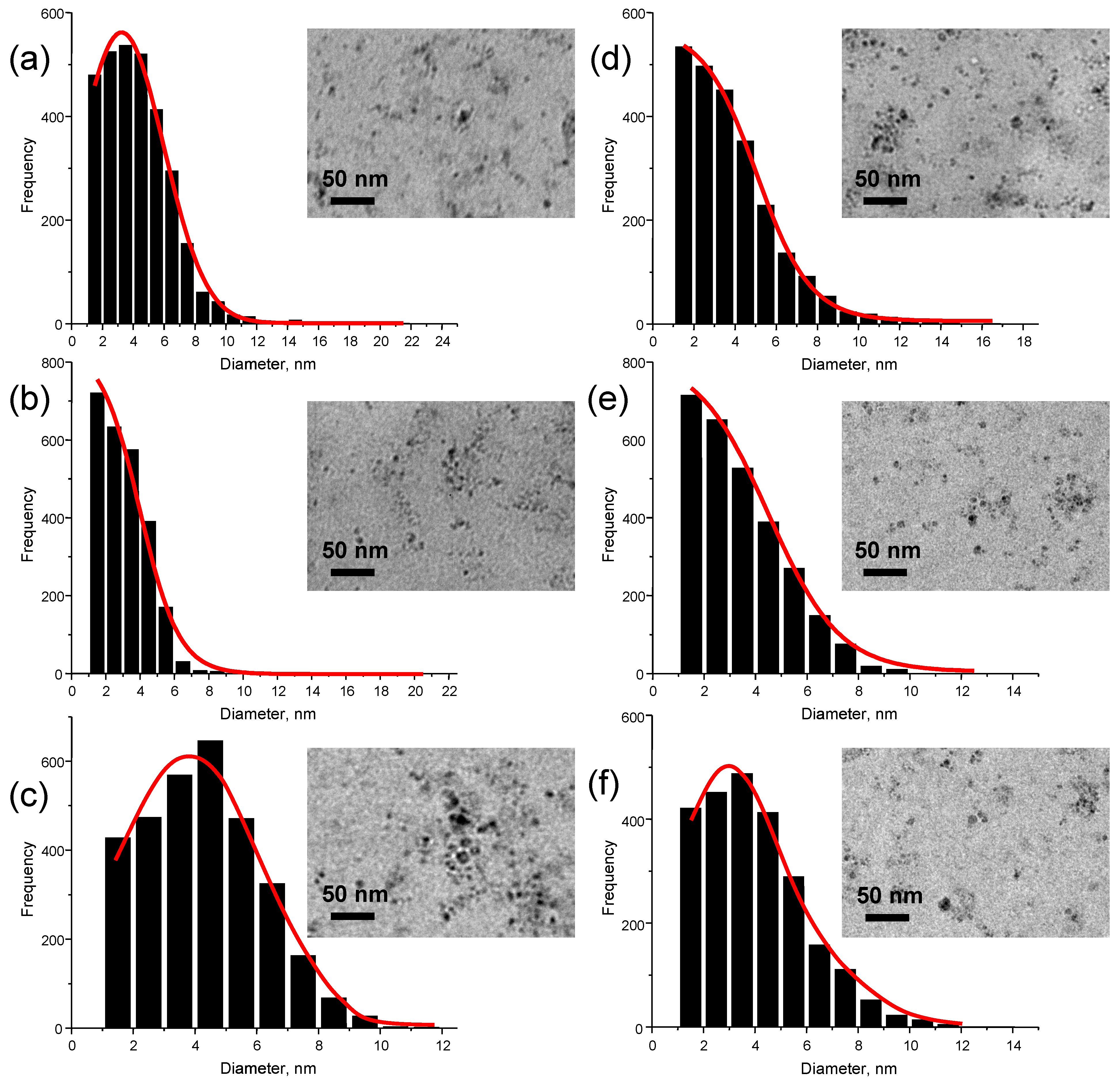
Abstract
:1. Introduction
2. Materials and Methods
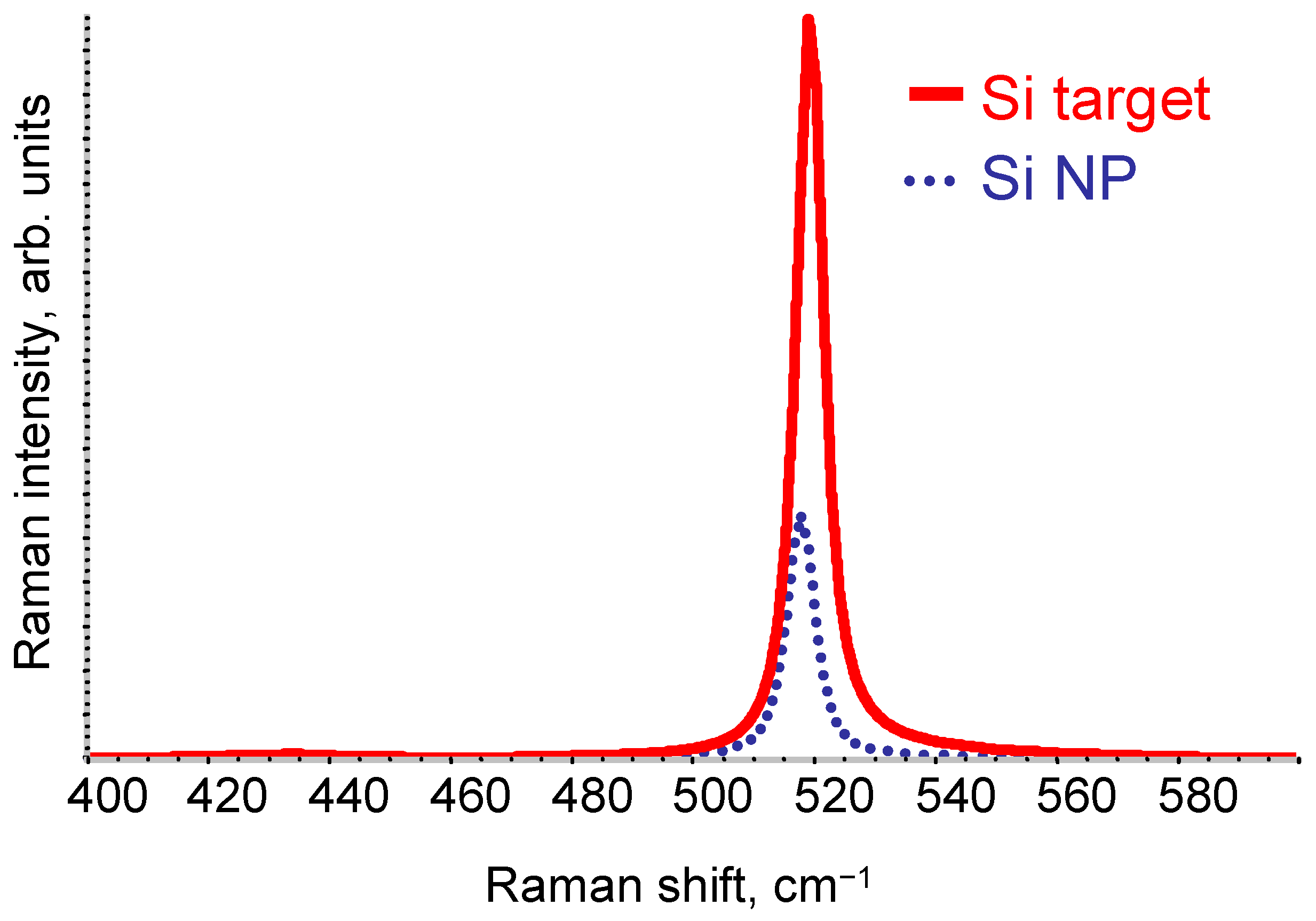
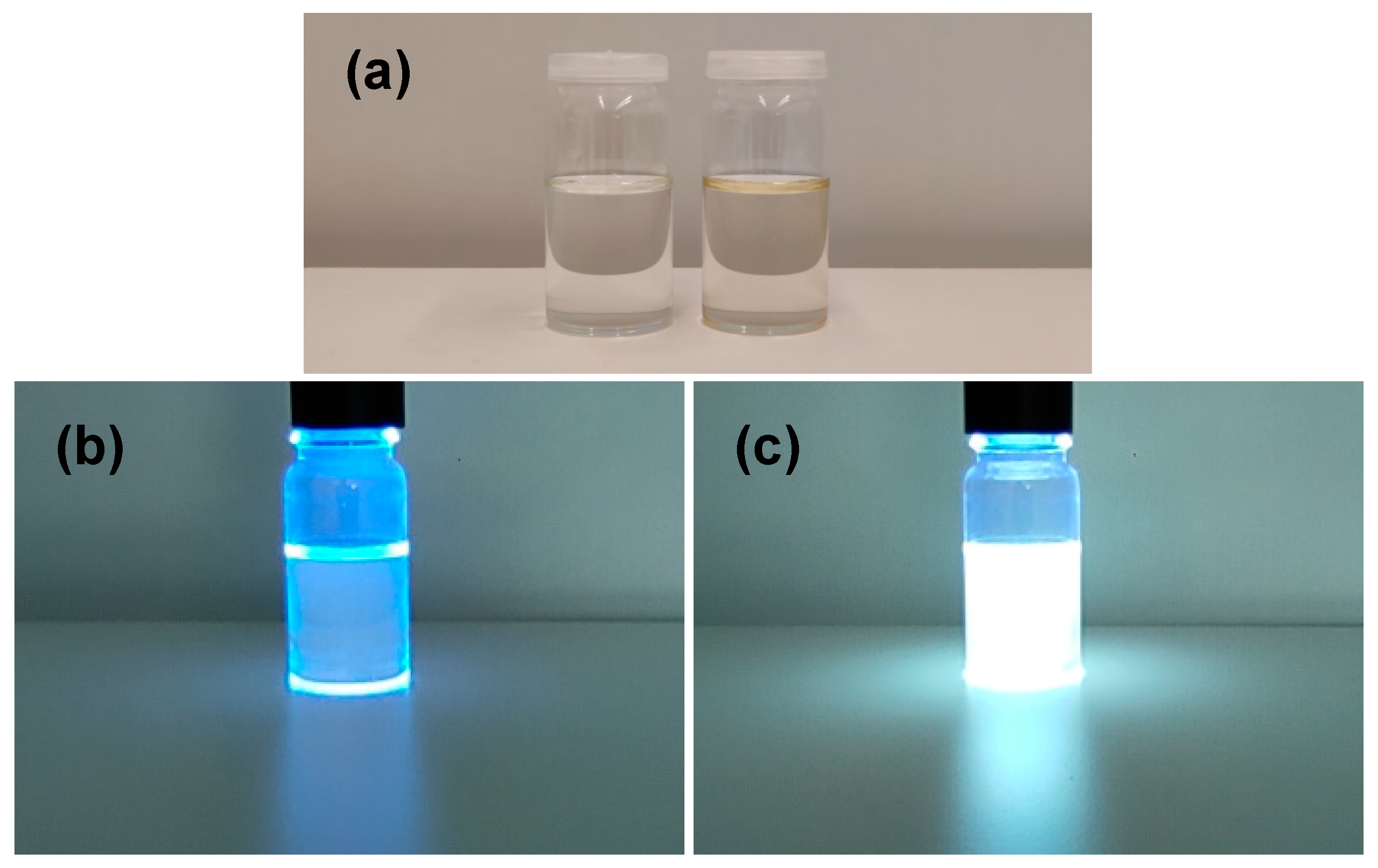
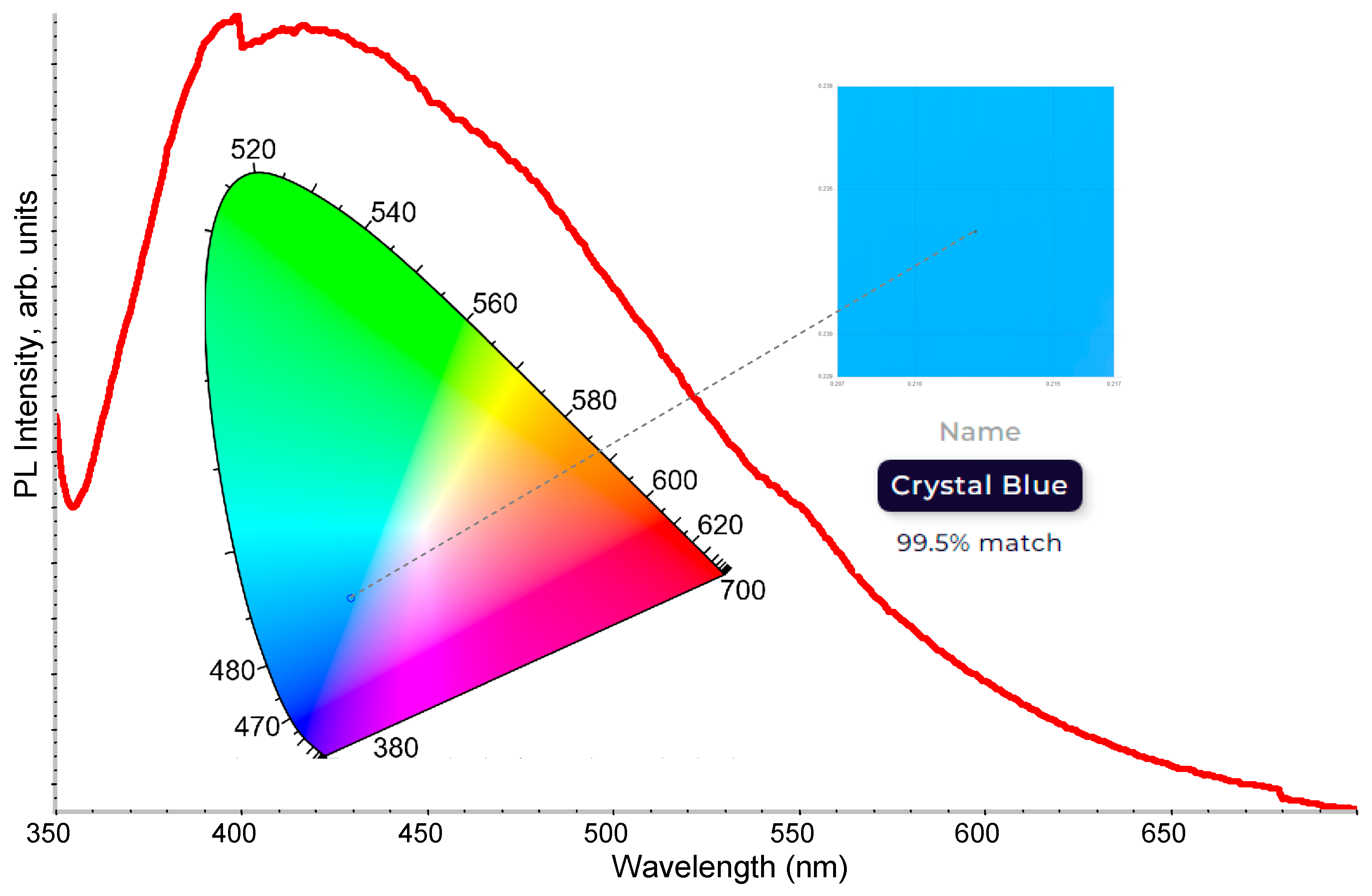
3. Results and Discussion
4. Conclusions
Author Contributions
Funding
Data Availability Statement
Acknowledgments
Conflicts of Interest
References
- Latella, R.; Gonzalez, A.J.; Bonifacio, D.A.; Kovylina, M.; Griol, A.; Benlloch, J.M.; Lecoq, P.; Konstantinou, G. Exploiting Cherenkov radiation with BGO-based metascintillators. IEEE Trans. Radiat. Plasma Med. Sci. 2023, 7, 810–818. [Google Scholar] [CrossRef]
- Korotchenko, K.; Eikhorn, Y.; Dabagov, S. Ultraviolet Cherenkov-Channeling Radiation by Protons. Radiat. Phys. Chem. 2020, 171, 108719. [Google Scholar] [CrossRef]
- Adriani, O.; Albergo, S.; D’Alessandro, R.; Lenzi, P.; Sciuto, A.; Starodubtsev, O.; Tricomi, A. CLASSiC: Cherenkov light detection with silicon carbide. Nucl. Instrum. Methods Phys. Res. Sect. A Accel. Spectrometers Detect. Assoc. Equip. 2017, 845, 439–442. [Google Scholar] [CrossRef]
- Cabrera, B.; Clarke, R.; Miller, A.; Nam, S.W.; Romani, R.; Saab, T.; Young, B. Cryogenic detectors based on superconducting transition-edge sensors for time-energy-resolved single-photon counters and for dark matter searches. Phys. B Condens. Matter 2000, 280, 509–514. [Google Scholar] [CrossRef]
- Kurinsky, N.; Yu, T.C.; Hochberg, Y.; Cabrera, B. Diamond detectors for direct detection of sub-GeV dark matter. Phys. Rev. D 2019, 99, 123005. [Google Scholar] [CrossRef]
- Gaitskell, R.J. Direct detection of dark matter. Annu. Rev. Nucl. Part. Sci. 2004, 54, 315–359. [Google Scholar] [CrossRef]
- Ota, R. Photon counting detectors and their applications ranging from particle physics experiments to environmental radiation monitoring and medical imaging. Radiol. Phys. Technol. 2021, 14, 134–148. [Google Scholar] [CrossRef]
- Grupen, C. Physics of particle detection. AIP Conf. Proc. 2000, 536, 3–34. [Google Scholar]
- Bader, N.; Kasim, S. Preparation and Investigation of TiO2, SnSx, and SnO2 Thin Film Properties for Use as UV Detectors. Basrah J. Sci. 2022, 40, 400–423. [Google Scholar] [CrossRef]
- Park, H.L.; Kim, H.; Lim, D.; Zhou, H.; Kim, Y.H.; Lee, Y.; Park, S.; Lee, T.W. Retina-inspired carbon nitride-based photonic synapses for selective detection of UV light. Adv. Mater. (Weinh. Ger.) 2020, 32, 1906899. [Google Scholar] [CrossRef]
- Meng, J.; Li, Z. Schottky-contacted nanowire sensors. Adv. Mater. (Weinh. Ger.) 2020, 32, 2000130. [Google Scholar] [CrossRef] [PubMed]
- Zhang, X.-Y.; Yang, Y.-S.; Wang, W.; Jiao, Q.-C.; Zhu, H.-L. Fluorescent sensors for the detection of hydrazine in environmental and biological systems: Recent advances and future prospects. Coord. Chem. Rev. 2020, 417, 213367. [Google Scholar] [CrossRef]
- Rachman, F.Z.; Hendrantoro, G. Optimization of A Fire Detection System Based on Radial Sector Scanning Using An UV Sensor. IEEE Sens. Lett. 2022, 7, 1–4. [Google Scholar] [CrossRef]
- Truong, C.T.; Nguyen, T.H.; Vu, V.Q.; Do, V.H.; Nguyen, D.T. Enhancing fire detection technology: A UV-based system utilizing fourier spectrum analysis for reliable and accurate fire detection. Appl. Sci. 2023, 13, 7845. [Google Scholar] [CrossRef]
- Khan, F.; Xu, Z.; Sun, J.; Khan, F.M.; Ahmed, A.; Zhao, Y. Recent advances in sensors for fire detection. Sensors 2022, 22, 3310. [Google Scholar] [CrossRef] [PubMed]
- Kinefuchi, K.; Koga, K.; Kusawake, H.; Tsuchiya, Y.; Kubota, K.; Cho, S.; Sano, T.; Fukatsu, T.; Terakado, Y.; Hatta, S. On-board Plasma Plume Diagnostics for ETS-9 All-electric Satellite. In Proceedings of the 36th International Electric Propulsion Conference, University of Vienna, Vienna, Austria, 15–20 September 2019. [Google Scholar]
- Béquin, P.; Nanda Tonlio, A.; Durand, S. Air plasma sensor for the measurement of sound pressure using millimetric and micrometric discharges. J. Appl. Phys. 2020, 127, 034502. [Google Scholar] [CrossRef]
- Velásquez-García, L.F.; Izquierdo-Reyes, J.; Kim, H. Review of in-space plasma diagnostics for studying the Earth’s ionosphere. J. Phys. D Appl. Phys. 2022, 55, 263001. [Google Scholar] [CrossRef]
- Blumenthal, D.J. Photonic integration for UV to IR applications. APL Photonics 2020, 5, 020903. [Google Scholar] [CrossRef]
- Li, Z.; Yan, T.; Fang, X. Low-dimensional wide-bandgap semiconductors for UV photodetectors. Nat. Rev. Mater. 2023, 8, 587–603. [Google Scholar] [CrossRef]
- Kang, C.H.; Trichili, A.; Alkhazragi, O.; Zhang, H.; Subedi, R.C.; Guo, Y.; Mitra, S.; Shen, C.; Roqan, I.S.; Ng, T.K. Ultraviolet-to-blue color-converting scintillating-fibers photoreceiver for 375-nm laser-based underwater wireless optical communication. Opt. Express 2019, 27, 30450–30461. [Google Scholar] [CrossRef]
- Li, Y.; Zheng, W.; Huang, F. All-silicon photovoltaic detectors with deep ultraviolet selectivity. PhotoniX 2020, 1, 15. [Google Scholar] [CrossRef]
- Klas, R.; Kirsche, A.; Gebhardt, M.; Buldt, J.; Stark, H.; Hädrich, S.; Rothhardt, J.; Limpert, J. Ultra-short-pulse high-average-power megahertz-repetition-rate coherent extreme-ultraviolet light source. PhotoniX 2021, 2, 4. [Google Scholar] [CrossRef]
- Zhang, D.; Zheng, W.; Lin, R.; Li, Y.; Huang, F. Ultrahigh EQE (15%) solar-blind UV photovoltaic detector with organic–inorganic heterojunction via dual built-in fields enhanced photogenerated carrier separation efficiency mechanism. Adv. Funct. Mater. 2019, 29, 1900935. [Google Scholar] [CrossRef]
- Capasso, M.; Acerbi, F.; Borghi, G.; Ficorella, A.; Furlan, N.; Mazzi, A.; Merzi, S.; Mozharov, V.; Regazzoni, V.; Zorzi, N. FBK VUV-sensitive Silicon Photomultipliers for cryogenic temperatures. Nucl. Instrum. Methods Phys. Res. Sect. A Accel. Spectrometers Detect. Assoc. Equip. 2020, 982, 164478. [Google Scholar] [CrossRef]
- Acerbi, F.; Paternoster, G.; Capasso, M.; Marcante, M.; Mazzi, A.; Regazzoni, V.; Zorzi, N.; Gola, A. Silicon photomultipliers: Technology optimizations for ultraviolet, visible and near-infrared range. Instruments 2019, 3, 15. [Google Scholar] [CrossRef]
- Moisello, E.; Malcovati, P.; Bonizzoni, E. Thermal sensors for contactless temperature measurements, occupancy detection, and automatic operation of appliances during the COVID-19 pandemic: A review. Micromachines 2021, 12, 148. [Google Scholar] [CrossRef]
- Huang, C.-Y.; Huang, C.-P.; Chen, H.; Pai, S.-W.; Wang, P.-J.; He, X.-R.; Chen, J.-C. A self-powered ultraviolet photodiode using an amorphous InGaZnO/p-silicon nanowire heterojunction. Vacuum 2020, 180, 109619. [Google Scholar] [CrossRef]
- Liu, Z.; Tang, W. A review of Ga2O3 deep-ultraviolet metal-semiconductor Schottky photodiodes. J. Phys. D Appl. Phys. 2023, 56, 093002. [Google Scholar] [CrossRef]
- Jerram, P.; Stefanov, K. CMOS and CCD image sensors for space applications. In High Performance Silicon Imaging; Elsevier: Amsterdam, The Netherlands, 2020; pp. 255–287. [Google Scholar]
- Onaka-Masada, A.; Kadono, T.; Okuyama, R.; Hirose, R.; Kobayashi, K.; Suzuki, A.; Koga, Y.; Kurita, K. Reduction of dark current in CMOS image sensor pixels using hydrocarbon-molecular-ion-implanted double epitaxial Si wafers. Sensors 2020, 20, 6620. [Google Scholar] [CrossRef]
- Aggarwal, N.; Gupta, G. Enlightening gallium nitride-based UV photodetectors. J. Mater. Chem. C 2020, 8, 12348–12354. [Google Scholar] [CrossRef]
- Hessel, C.M.; Reid, D.; Panthani, M.G.; Rasch, M.R.; Goodfellow, B.W.; Wei, J.; Fujii, H.; Akhavan, V.; Korgel, B.A. Synthesis of ligand-stabilized silicon nanocrystals with size-dependent photoluminescence spanning visible to near-infrared wavelengths. Chem. Mater. 2012, 24, 393–401. [Google Scholar] [CrossRef]
- Li, Q.; Jin, R. Photoluminescence from colloidal silicon nanoparticles: Significant effect of surface. Nanotechnol. Rev. 2017, 6, 601–612. [Google Scholar] [CrossRef]
- Miyano, M.; Kitagawa, Y.; Wada, S.; Kawashima, A.; Nakajima, A.; Nakanishi, T.; Ishioka, J.; Shibayama, T.; Watanabe, S.; Hasegawa, Y. Photophysical properties of luminescent silicon nanoparticles surface-modified with organic molecules via hydrosilylation. Photochem. Photobiol. Sci. 2016, 15, 99–104. [Google Scholar] [CrossRef] [PubMed]
- Park, N.-M.; Choi, C.-J.; Seong, T.-Y.; Park, S.-J. Quantum confinement in amorphous silicon quantum dots embedded in silicon nitride. Phys. Rev. Lett. 2001, 86, 1355. [Google Scholar] [CrossRef]
- Kumar, M.J.; Singh, T.V. Quantum confinement effects in strained silicon mosfets. Int. J. Nanosci. 2008, 7, 81–84. [Google Scholar] [CrossRef]
- Mastronardi, M.L.; Maier-Flaig, F.; Faulkner, D.; Henderson, E.J.; Kübel, C.; Lemmer, U.; Ozin, G.A. Size-dependent absolute quantum yields for size-separated colloidally-stable silicon nanocrystals. Nano Lett. 2012, 12, 337–342. [Google Scholar] [CrossRef]
- Baldwin, R.K.; Pettigrew, K.A.; Ratai, E.; Augustine, M.P.; Kauzlarich, S.M. Solution reduction synthesis of surface stabilized silicon nanoparticles. Chem. Commun. 2002, 2022, 1822–1823. [Google Scholar] [CrossRef]
- Kobayashi, H.; Chewchinda, P.; Ohtani, H.; Odawara, O.; Wada, H. Effects of laser energy density on silicon nanoparticles produced using laser ablation in liquid. J. Phys. Conf. Ser. 2013, 441, 012035. [Google Scholar] [CrossRef]
- Tan, D.; Ma, Z.; Xu, B.; Dai, Y.; Ma, G.; He, M.; Jin, Z.; Qiu, J. Surface passivated silicon nanocrystals with stable luminescence synthesized by femtosecond laser ablation in solution. Phys. Chem. Chem. Phys. 2011, 13, 20255–20261. [Google Scholar] [CrossRef]
- Heintz, A.S.; Fink, M.J.; Mitchell, B.S. Mechanochemical synthesis of blue luminescent alkyl/alkenyl-passivated silicon nanoparticles. Adv. Mater. (Weinh. Ger.) 2007, 19, 3984–3988. [Google Scholar] [CrossRef]
- Lam, C.; Zhang, Y.; Tang, Y.; Lee, C.; Bello, I.; Lee, S. Large-scale synthesis of ultrafine Si nanoparticles by ball milling. J. Cryst. Growth 2000, 220, 466–470. [Google Scholar] [CrossRef]
- Zhang, X.; Min, B.-I.; Wang, Y.; Hayashida, R.; Tanaka, M.; Watanabe, T. Preparation of carbon-coated silicon nanoparticles with different hydrocarbon gases in induction thermal plasma. J. Phys. Chem. C 2021, 125, 15551–15559. [Google Scholar] [CrossRef]
- Kramer, N.; Anthony, R.; Mamunuru, M.; Aydil, E.; Kortshagen, U. Plasma-induced crystallization of silicon nanoparticles. J. Phys. D Appl. Phys. 2014, 47, 075202. [Google Scholar] [CrossRef]
- Choi, J.; Kim, K.; Han, H.-s.; Hwang, M.P.; Lee, K.H. Electrochemical synthesis of red fluorescent silicon nanoparticles. Bull. Korean Chem. Soc. 2014, 35, 35–38. [Google Scholar] [CrossRef]
- Zhou, J.; Jiang, Z.; Cai, W.; Liu, X.; Zhu, Y.; Lan, Y.; Ma, K.; Qian, Y. Solvothermal synthesis of a silicon hierarchical structure composed of 20 nm Si nanoparticles coated with carbon for high performance Li-ion battery anodes. Dalton Trans. 2016, 45, 13667–13670. [Google Scholar] [CrossRef] [PubMed]
- Bhat, J.A.; Rajora, N.; Raturi, G.; Sharma, S.; Dhiman, P.; Sanand, S.; Shivaraj, S.; Sonah, H.; Deshmukh, R. Silicon nanoparticles (SiNPs) in sustainable agriculture: Major emphasis on the practicality, efficacy and concerns. Nanoscale Adv. 2021, 3, 4019–4028. [Google Scholar] [CrossRef]
- Keshavarz, M.; Tan, B.; Venkatakrishnan, K. Functionalized stress component onto bio-template as a pathway of cytocompatibility. Sci. Rep. 2016, 6, 35425. [Google Scholar] [CrossRef]
- Keshavarz, M.; Tan, B.; Venkatakrishnan, K. Multiplex photoluminescent silicon nanoprobe for diagnostic bioimaging and intracellular analysis. Adv. Sci. 2018, 5, 1700548. [Google Scholar] [CrossRef]
- Semaltianos, N.; Logothetidis, S.; Perrie, W.; Romani, S.; Potter, R.; Edwardson, S.; French, P.; Sharp, M.; Dearden, G.; Watkins, K. Silicon nanoparticles generated by femtosecond laser ablation in a liquid environment. J. Nanopart. Res. 2010, 12, 573–580. [Google Scholar] [CrossRef]
- Amoruso, S.; Bruzzese, R.; Spinelli, N.; Velotta, R.; Vitiello, M.; Wang, X.; Ausanio, G.; Iannotti, V.; Lanotte, L. Generation of silicon nanoparticles via femtosecond laser ablation in vacuum. Appl. Phys. Lett. 2004, 84, 4502–4504. [Google Scholar] [CrossRef]
- Berg, S.; Kutra, D.; Kroeger, T.; Straehle, C.N.; Kausler, B.X.; Haubold, C.; Schiegg, M.; Ales, J.; Beier, T.; Rudy, M. Ilastik: Interactive machine learning for (bio) image analysis. Nat. Methods 2019, 16, 1226–1232. [Google Scholar] [CrossRef]
- Faraci, G.; Gibilisco, S.; Pennisi, A.R.; Faraci, C. Quantum size effects in Raman spectra of Si nanocrystals. J. Appl. Phys. 2011, 109, 074311. [Google Scholar] [CrossRef]
- Faraci, G.; Gibilisco, S.; Russo, P.; Pennisi, A.R.; La Rosa, S. Modified Raman confinement model for Si nanocrystals. Phys. Rev. B 2006, 73, 033307. [Google Scholar] [CrossRef]
- Lee, S.; Cho, W.J.; Han, I.K.; Choi, W.J.; Lee, J.I. White light emitting silicon nanocrystals as nanophosphor. Phys. Status Solidi B 2004, 241, 2767–2770. [Google Scholar] [CrossRef]
- Li, Q.; Luo, T.-Y.; Zhou, M.; Abroshan, H.; Huang, J.; Kim, H.J.; Rosi, N.L.; Shao, Z.; Jin, R. Silicon nanoparticles with surface nitrogen: 90% quantum yield with narrow luminescence bandwidth and the ligand structure based energy law. ACS Nano 2016, 10, 8385–8393. [Google Scholar] [CrossRef] [PubMed]
- Ruan, J.; Fauchet, P.; Dal Negro, L.; Cazzanelli, M.; Pavesi, L. Stimulated emission in nanocrystalline silicon superlattices. Appl. Phys. Lett. 2003, 83, 5479–5481. [Google Scholar] [CrossRef]
- Pavesi, L.; Dal Negro, L.; Mazzoleni, C.; Franzo, G.; Priolo, D.F. Optical gain in silicon nanocrystals. Nature 2000, 408, 440–444. [Google Scholar] [CrossRef]
- Sun, W.; Qian, C.; Wang, L.; Wei, M.; Mastronardi, M.L.; Casillas, G.; Breu, J.; Ozin, G.A. Switching-on quantum size effects in silicon nanocrystals. Adv. Mater. (Weinh. Ger.) 2015, 27, 746–749. [Google Scholar] [CrossRef]
- Sahi, S.; Magill, S.; Ma, L.; Xie, J.; Chen, W.; Jones, B.; Nygren, D. Wavelength-shifting properties of luminescence nanoparticles for high energy particle detection and specific physics process observation. Sci. Rep. 2018, 8, 10515. [Google Scholar] [CrossRef]
- Chen, W.; Li, G.; Malm, J.-O.; Huang, Y.; Wallenberg, R.; Han, H.; Wang, Z.; Bovin, J.-O. Pressure dependence of Mn2+ fluorescence in ZnS: Mn2+ nanoparticles. J. Lumin. 2000, 91, 139–145. [Google Scholar] [CrossRef]
- Hossu, M.; Schaeffer, R.O.; Ma, L.; Chen, W.; Zhu, Y.; Sammynaiken, R.; Joly, A.G. On the luminescence enhancement of Mn2+ by co-doping of Eu2+ in ZnS: Mn, Eu. Opt. Mater. 2013, 35, 1513–1519. [Google Scholar] [CrossRef]
- Chen, W.; Grouquist, D.; Roark, J. Voltage tunable electroluminescence of CdTe nanoparticle light-emitting diodes. J. Nanosci. Nanotechnol. 2002, 2, 47–53. [Google Scholar] [CrossRef] [PubMed]
- Ma, L.; Chen, W.; Schatte, G.; Wang, W.; Joly, A.G.; Huang, Y.; Sammynaiken, R.; Hossu, M. A new Cu–cysteamine complex: Structure and optical properties. J. Mater. Chem. C 2014, 2, 4239–4246. [Google Scholar] [CrossRef]
- Liu, Y.; Chen, W.; Wang, S.; Joly, A.G.; Westcott, S.; Woo, B.K. X-ray luminescence of LaF3: Tb3+ and LaF3: Ce3+, Tb3+ water-soluble nanoparticles. J. Appl. Phys. 2008, 103, 063105. [Google Scholar] [CrossRef]
- Magill, S.; Nayfeh, M.; Fizari, M.; Malloy, J.; Maximenko, Y.; Xie, J.; Yu, H. Enhanced UV light detection using wavelength-shifting properties of Silicon nanoparticles. J. Instrum. 2015, 10, P05008. [Google Scholar] [CrossRef]


Disclaimer/Publisher’s Note: The statements, opinions and data contained in all publications are solely those of the individual author(s) and contributor(s) and not of MDPI and/or the editor(s). MDPI and/or the editor(s) disclaim responsibility for any injury to people or property resulting from any ideas, methods, instructions or products referred to in the content. |
© 2023 by the authors. Licensee MDPI, Basel, Switzerland. This article is an open access article distributed under the terms and conditions of the Creative Commons Attribution (CC BY) license (https://creativecommons.org/licenses/by/4.0/).
Share and Cite
Lazauskas, A.; Gimžauskaitė, D.; Ilickas, M.; Marcinauskas, L.; Aikas, M.; Abakevičienė, B.; Volyniuk, D. Laser Ablation of Silicon Nanoparticles and Their Use in Charge-Coupled Devices for UV Light Sensing via Wavelength-Shifting Properties. Nanomaterials 2023, 13, 2915. https://0-doi-org.brum.beds.ac.uk/10.3390/nano13222915
Lazauskas A, Gimžauskaitė D, Ilickas M, Marcinauskas L, Aikas M, Abakevičienė B, Volyniuk D. Laser Ablation of Silicon Nanoparticles and Their Use in Charge-Coupled Devices for UV Light Sensing via Wavelength-Shifting Properties. Nanomaterials. 2023; 13(22):2915. https://0-doi-org.brum.beds.ac.uk/10.3390/nano13222915
Chicago/Turabian StyleLazauskas, Algirdas, Dovilė Gimžauskaitė, Mindaugas Ilickas, Liutauras Marcinauskas, Mindaugas Aikas, Brigita Abakevičienė, and Dmytro Volyniuk. 2023. "Laser Ablation of Silicon Nanoparticles and Their Use in Charge-Coupled Devices for UV Light Sensing via Wavelength-Shifting Properties" Nanomaterials 13, no. 22: 2915. https://0-doi-org.brum.beds.ac.uk/10.3390/nano13222915