Article

Ultraviolet-Ozone Treatment: An Effective Method for Fine-Tuning Optical and Electrical Properties of Suspended and Substrate-Supported MoS2

1
School of Physics, Engineering and Technology, University of York, Heslington, York YO10 5DD, UK
2
Department of Physics, Faculty of Science, Istanbul University, Vezneciler, Istanbul 34134, Turkey
3
Institut d’Electronique, Microelectronique & Nanotechnologie IEMN CNRS UMR 8520, Université Polytechnique Hauts de France, 59313 Valenciennes, France
*
Authors to whom correspondence should be addressed.
Nanomaterials 2023, 13(23), 3034; https://0-doi-org.brum.beds.ac.uk/10.3390/nano13233034
Submission received: 21 October 2023 / Revised: 23 November 2023 / Accepted: 24 November 2023 / Published: 27 November 2023

Abstract

:
Ultraviolet-ozone (UV-O3) treatment is a simple but effective technique for surface cleaning, surface sterilization, doping, and oxidation, and is applicable to a wide range of materials. In this study, we investigated how UV-O3 treatment affects the optical and electrical properties of molybdenum disulfide (MoS2), with and without the presence of a dielectric substrate. We performed detailed photoluminescence (PL) measurements on 1–7 layers of MoS2 with up to 8 min of UV-O3 exposure. Density functional theory (DFT) calculations were carried out to provide insight into oxygen-MoS2 interaction mechanisms. Our results showed that the influence of UV-O3 treatment on PL depends on whether the substrate is present, as well as the number of layers. Additionally, 4 min of UV-O3 treatment was found to be optimal to produce p-type MoS2, while maintaining above 80% of the PL intensity and the emission wavelength, compared to pristine flakes (intrinsically n-type). UV-O3 treatment for more than 6 min not only caused a reduction in the electron density but also deteriorated the hole-dominated transport. It is revealed that the substrate plays a critical role in the manipulation of the electrical and optical properties of MoS2, which should be considered in future device fabrication and applications.

1. Introduction

In recent years, semiconducting two-dimensional transition metal dichalcogenides (2D-TMDs) have become a group of highly demanded materials for next-generation optoelectronic devices such as photodetectors and light emitters [1,2,3,4] because of their unique optical, electronic, and structural properties. Despite many advantages of these semiconducting materials, there are some drawbacks such as low carrier concentration and mobility, which result in low electrical conductivity [5,6] compared to the materials already widely used in electronic/optoelectronic technologies, such as Si and GaAs. To realize high-performance optoelectronic devices, both n-type and p-type semiconducting 2D-TMDs are required [7,8]. Conventional doping techniques used for semiconductors are not suitable for 2D materials because they modify their crystal structures and result in a significant deterioration of their optoelectrical properties [9]. On the other hand, thanks to the atomic thickness of 2D-TMDs, their optical and structural properties as well as carrier dynamics can be efficiently engineered using different post-growth methods [10]. Surface charge transfer-based doping [11], substitutional doping [12], interstitial doping [13], and vacancy-based doping [14] are the main post-growth doping mechanisms for 2D-TMDs [15]. Based on these mechanisms, there are several reported doping techniques such as chemical treatment [13], ion implantation [16], plasma doping [17], thermal annealing [18], electron beam irradiation [19], and ultraviolet-ozone (UV-O3) treatment [20], which aim to achieve n- and/or p-type doping. Due to the high sensitivity of 2D materials’ properties, the main challenge in post-growth doping is to maintain their superb optoelectrical properties for device applications, while controlling the doping concentration with consistency. In this study, we focus on the effect of UV-O3 treatment on the optical and electrical properties of MoS2, which leads to p-type doping of the TMD material.
UV-O3 treatment is a useful process for a wide range of materials for surface modification [21]. It has been employed as an effective tool for defect engineering and doping in graphene and 2D TMDs. There are a few studies in the literature on UV-O3-induced p-type doping on graphene [22,23,24]. Liang et al. presented controllable p-type doping in a range of semiconducting TMDs (MoTe2, WSe2, MoSe2, and PtSe2) and proposed three mechanisms for UV-O3-induced hole doping: (1) charge transfer due to the interaction with oxygen molecules, (2) isoelectronic substitution of chalcogen atoms with oxygen atoms, and (3) charge transport over the oxide surface due to the transition metal oxide formation (MoO3, WO3 etc.) [20]. Zheng et al. showed that UV-O3 treatment is an effective method for p-type doping of MoTe2 field-effect transistors and it enhances its electrical performance enormously. The hole concentration and mobility are enhanced by nearly two orders of magnitude, and the conductivity by five orders of magnitude [25]. These promising studies are focused on the effect of UV-O3 treatment on the electrical properties of TMDs only. In 2D-TMD optoelectronic devices, the effect of UV-O3 treatment on their optical properties is also critical. There are only a few studies about the effect of UV-O3 treatment on the optical properties of semiconducting TMDs. Yang et al. reported that PL intensity of pristine exfoliated MoS2 decreased and was eventually quenched as UV-O3 exposure time increased from 0 to 10 min, which was attributed to the structural degradation [26]. The quenching of PL was also observed on chemical vapour deposited and exfoliated monolayer MoS2 [27] and on exfoliated monolayer WS2 and WSe2 as a result of 6 min of UV-O3 treatment due to oxidation [28]. On the other hand, Zheng et al. showed a 37-fold increment in the PL intensity by converting trilayer MoSe2 to monolayer with 7 min of UV-O3 treatment [29]. While the effect of UV-O3 on the electrical properties is consistent from one study to another, there is a contradiction about the effect of UV-O3 treatment on the optical properties of 2D-TMDs. More importantly, there is no systematic study on the effect of UV-O3 treatment on suspended, or multi-layer TMDs. Although monolayer (ML) TMDs have the strongest emission, the effect on few-layer TMDs is also important for the potential electronic and optoelectronic devices.
In this paper, we reveal that the effect of UV-O3 treatment does not only depend on the type of materials but also the number of layers and the substrate (the environment). To investigate the layer and substrate dependency of the UV-O3 treatment on the optical properties of semiconducting TMDs, we fabricated suspended and substrate-supported MoS2 samples with different numbers of layers from monolayer to seven layers. PL spectroscopy was carried out to investigate the effect on their optical properties with a range of UV-O3 exposure time. Density functional theory (DFT) calculations were performed to understand which oxygen-related mechanism during the UV-O3 exposure could cause p-type doping via charge trapping, as well as the role of intrinsic sulphur defects. Further electrical characterisation was performed on a 4L-MoS2 transistor to investigate how the carrier dynamics can be modified using the UV-O3 treatment.

2. Experimental Methods

E-beam lithography was used to pattern the squares (4 μm × 4 μm) on Polymethyl methacrylate (PMMA)-coated Si3N4 (150 nm)-on-SiO2 substrates. Patterned squares were etched 300 nm in depth with a Reactive Ion Etcher, using a mixture gas of CHF3 and O2. Resist was removed with a resist remover (1165) and acetone, and the substrate was rinsed in isopropyl alcohol (IPA) before drying. Bulk single-crystal MoS2 was purchased from HQ Graphene, which was intrinsically n-doped. Scotch tape and polydimethylsiloxane (PDMS)-assisted mechanical exfoliation method was used to obtain MoS2 flakes with different numbers of layers. The flakes larger than 10 μm × 10 μm were transferred either onto the etched squares to be suspended or the flat area of the Si3N4-on-SiO2 substrates.
The PL spectra of the flakes were measured using a microPL setup equipped with an Andor iDus detector and a 532 nm excitation laser, before and after UV-O3 treatment. The laser beam was focused to be a spot of ~1.5 μm in diameter, fitting inside the suspended areas. The UV-O3 treatment was performed (Jelight, 30 mW/cm2 at a wavelength of 254 nm) for different periods of time.
DFT calculations were undertaken on four-layer MoS2 using a plane wave basis set, as implemented in the VASP package [30,31,32]. A gamma-centred Monkhorst-Pack grid of 2 × 2 × 1 k points was used to sample the Brillouin zone for all calculations, with geometry optimizations performed to a force tolerance of 0.01 eV/Å. Ideal values of D3 parameters for HSE06 are still an open area of research and could therefore not be sourced from the literature, so in this study, we used parameters quoted for the related hybrid functional PBE0 for calculations. Version 5.2 PBE plane wave potentials (PAW) were used for all calculations, with a plane wave cut-off value of 520 eV.
Preliminary geometry optimizations were undertaken with the Perdew–Burke–Ernzerhof (PBE) functional [33], including Grimme’s D3 van der Waals corrections [34] to determine the lowest energy adsorption site and adsorbate bond orientations. Further calculations of the band structures, including substitutional defects, were undertaken using the HSE06 functional with D3 corrections, ensuring more accurate energy levels to fully capture any charge-trapping levels [35]. These calculations were initially optimized with one extra electron added to capture the geometry of the charged structure, then reoptimized for the neutral case. This enabled Bader charge analysis to be conducted on both neutral and charged cases to identify if the charged case differed greatly at the defect site, which would be indicative of charge trapping. To reduce the defect density and prevent bands forming from the defect levels, the unit cell used was double the size of the primitive cell in the a and b directions. A vacuum gap of 20 Å was employed to minimize interaction between periodically repeated slabs.
The band structure was also calculated for a pristine four-layer MoS2 system at the HSE06 level, with the parameters described above and a high symmetry k-point path generated using the sumo package [36]. This was necessary to determine where the defect levels were relative to these bands. We note here that spin-orbit coupling was not included in any of these calculations; however, previous calculations on MoS2 have shown this to result in a 0.1 eV shift in the band gap—significantly lower than the energy difference between the CBM and defect levels found in this work—hence it would be unlikely to change any conclusions [37].
Defect formation energies were calculated for each defect as a function of the chemical potential of sulphur to determine which defects were most stable under different conditions—from sulphur-poor to sulphur-rich. These energies were calculated using Equation (1), where μi are the chemical potentials of species removed or added to the system and ni is the change in the number of these atoms, i = Mo, S or O.
Efdef = Edef − Ebulk − ∑niμi
Both sulphur-rich and sulphur-poor limits were considered at a constant oxygen chemical potential—with only 2 points necessary due to the clear linear nature of these energies with respect to one chemical potential. These limits were defined as the sulphur chemical potential, where μS = 1/2 ES2 and μMo = EMo for the sulphur-rich and sulphur-poor cases, respectively, as either of these conditions uniquely defines both μS and μMo according to Equation (2).
EMoS2 = μMo + 2µS
All energies used were calculated at PBE + D3 level of theory and the formation energies for O2 defects were halved to calculate per oxygen atom and ensure these energies are comparable between the different systems.
Electronic states with enhanced localization on oxygen-related defects were identified by examining coefficients in the projection of one-electron wavefunctions onto atoms. To ensure the corresponding band energies were consistent between different supercells, the lowest energy molybdenum core state in the pristine surface was a reference for aligning electronic structures. The densities of states were calculated on a grid of 2000 points and plotted using the sumo package [36].
In order to monitor the doping effect with different UV-O3 exposure times, a 4L-MoS2 field-effect transistor was fabricated. A 4L MoS2 flake was transferred on SiO2/Si wafer and e-beam lithography was used to pattern a Transfer Length Method (TLM) structure on the flake. Cr/Au (10 nm/60 nm) were deposited in a thermal evaporator, followed by a lift-off process. Electrical characterisation was carried out using an Agilent B2902A double-channel source-meter unit.

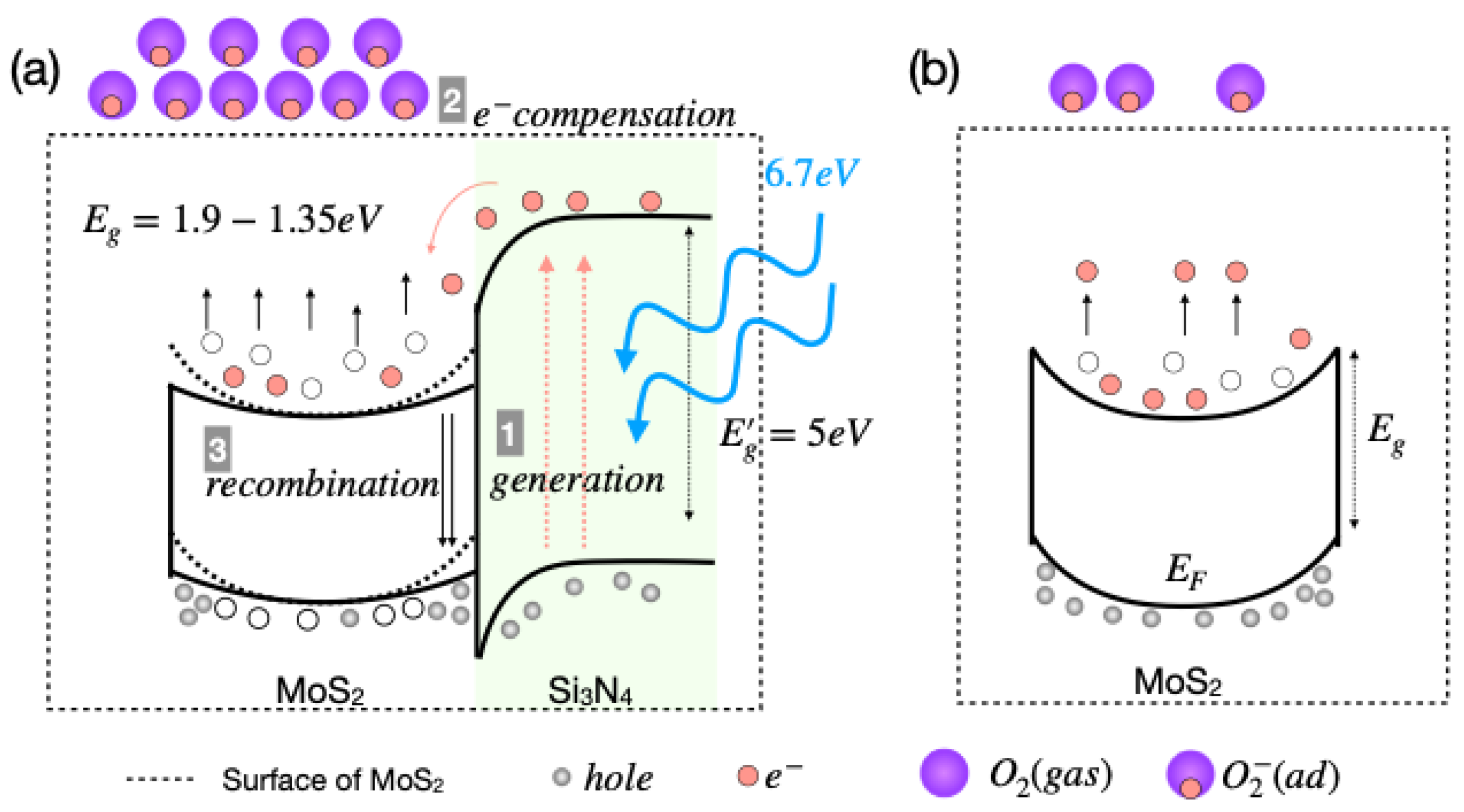
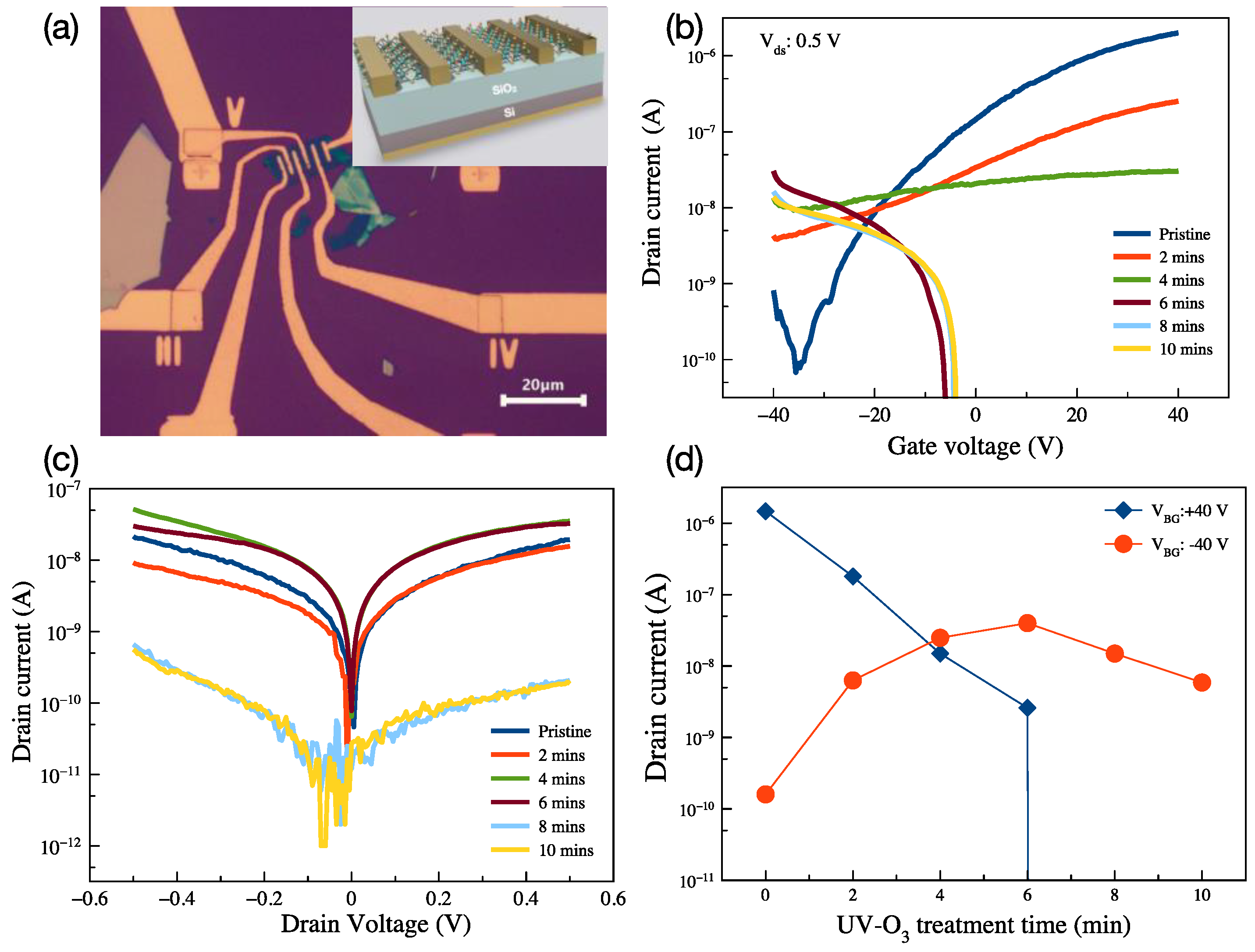
3. Results and Discussion

It is well known that the electronic band structure and energy bandgap of TMDs depend on the number of layers. The number of layers in MoS2 flakes can be precisely determined using the PL peak wavelength/energy. Flakes with different layer numbers were selectively transferred to the pre-patterned Si3N4 substrates. Figure 1a,b show a microscope image of the 4L MoS2 flake on the Si3N4 substrate, and a schematic drawing of the sample structure, respectively.
Optical properties of suspended and supported MoS2 flakes on Si3N4 were investigated using micro-PL spectroscopy. As a function of the number of layers (from a single layer to seven layers) the bandgap of the suspended MoS2 varies from ~1.90 eV to ~1.35 eV (Figure 1e). Up to 45 meV blueshifts in the PL peak energy were observed in the thicker supported flakes compared to the suspended flakes [38]. There are several studies on the substrate effect on the optical properties of 2D TMDs in the literature [39,40,41], although most of these studies were focused on the substrate effect on monolayer TMDs. The weaker, broader, and red-shifted PL from the TMDs transferred onto dielectric substrates can be attributed to the amount of moisture at the interface and/or interlayer charge transfer, which results in charge doping [41,42,43]. In Figure 1, we observe a consistent reduction in PL intensity for all layer numbers, and a small redshift of the peak energy in the thicker supported flakes compared to the suspended flakes. This can be explained by the possibility of more charge transfer in the thicker layers due to their lower energy bandgap [44].
Next, the effect of UV-O3 treatment on suspended and supported MoS2 as a function of number of layers and exposure time was investigated. The main purpose of our study is to understand the layer and substrate dependency of the UV-O3 treatment time on the optical properties of the 2D TMDs, ideally maintaining their photoluminescence. We chose the UV-O3 treatment times of 1, 4, 6, and 8 min on each sample. Each sample was exposed separately. Figure 2 shows the PL spectra of pristine and UV-O3-treated flakes. As UV-O3 treatment time increases, the PL intensity decreases for all samples. The intensity of the PL emission from the supported MoS2 decreases significantly with UV-O3 treatment time and is eventually fully quenched after 8 min., while the suspended flakes are less affected by the treatment. Figure 3 shows that there are clear differences in the trend between the suspended and supported flakes. In general, the thinner flakes are more sensitive to UV-O3 treatment for both cases, which is expected; however, for suspended flakes, up to 4 min of exposure for all thicknesses does not degrade the PL intensity significantly. We note that in some layers, the PL intensities after 4 min treatment are even higher than after 1 min treatment time, which is likely due to the small variation in PL intensities between consecutive measurements. The overall trend of above 4 min exposure time is, however, clear.
We use DFT calculations to understand the effect of UV-O3 on suspended TMDs. Conventional UV-O3 cleaners have two dominant UV peaks, at 184 nm and 254 nm. Upon irradiation, molecular oxygen (O2) present in the air is dissociated by radiation at 184 nm. This results in the formation of two radicals of singlet oxygen (O). These radicals continue to react with molecular oxygens forming molecules of ozone (O3). The simulations were carried out for these three species. Sulphur substitutional defects involving these species, as well as surface adsorption onto various non-symmetrically equivalent high symmetry sites, were considered. Both substitution and adsorption of O3 resulted in dissociation into an O defect and a free O2 molecule in the vacuum gap, which is therefore equivalent to the O defects. The formation energies were calculated with a constant oxygen chemical potential of half the energy of an oxygen atom, plotted in Figure 4a, which represents the stability of each type of defect as a function of sulphur chemical potential. In both the sulphur-rich and sulphur-poor extremes, no O2 defects were stable as their formation energies were above zero for all chemical potentials, hence O defects can be concluded to be the most likely defect to form in this system. In the sulphur-poor region, O2/S substitution is the most stable, and for all chemical potentials, O adsorption is the most stable scenario. Figure 4b shows that the unoccupied electronic states introduced by all these defects are higher in energy than the conduction band minimum (CBM) of pristine monolayer MoS2, meaning no PL shift should be induced by the defects. The O2 defects have higher formation energy than the O defects, which indicates that they are likely to be short-lived; however, these short-lived O2 defects could be relevant for providing mechanisms to form O defects. In Figure 4c, the excess Bader charge was shown as a function of the vertical position of each atom in the unit cell in the case of O adsorption and with one added electron. Low localization can be seen at both top and bottom surfaces, with the most localization on the sulphur atom closest to the adsorbed O atom. Even this larger localization is only 0.08 e, suggesting this localization is extremely weak and unlikely to trap enough charge to cause p-type doping. One singlet O adsorption between the TMD layers was also investigated at the PBE level (the lower level of theory) for both neutral and +1 electron systems. This gave similar charge densities and defect levels compared to O adsorption on the surface. We also note here that our DFT model reflects the substitution of one sulphur atom in the unit cell (Figure 4c), and the adsorption of one of the three oxygen species (O, O2, and O3) in the suspended 4L MoS2 system; it does not reflect multiple species adsorption or substitution of multiple sulphur atoms, which potentially happens with longer UV-O3 treatment time. The PL results from short-time UV-O3 treatment (1 to 4 min) show no significant reduction in the intensity nor any peak wavelength shift, which is consistent with our DFT results.
Inclusion of the substrate in the DFT calculations is too computationally time-consuming using the hybrid level of theory and requires taking into account extra parameters, such as surface roughness, optical interferences specifically on dielectric substrates, defects, and impurities on the interface, etc., which is considered to be future work.
To understand the effect of UV-O3 on the substrate-supported flakes, we analyzed the PL spectra of the 2L and 6L flakes in depth. The reduction in the PL intensities starts from higher energy on the supported 2L and 6L flakes with up to 6 min of UV-O3 treatment (see Figure 2a,c). This can be explained by carrier dynamics involving the presence of the Si3N4 substrate. The bandgap and photogenerated charge carriers of the substrate under UV irritation play a key role in this process. The bandgap of the Si3N4 is ~5 eV. During the UV-O3 exposure, the 184 nm characteristic radiation of the UV source can generate free electrons and holes in the substrate. The generated free electrons diffuse to MoS2, which has a lower energy level than that of the conduction band of Si3N4 in the heterostructure (illustrated in Figure 5a). Such diffusion compensates for the decreased electron density caused by the oxygen adsorption and allows more oxygen defect formation on the MoS2 surface. The transferred electrons also recombine with free holes in MoS2, resulting in non-radiative recombination at the interfaces of the flake and the substrate, hence further reduction in the PL intensity of the supported MoS2. Moreover, we observed an 11 meV redshift in the PL peak energy of the 4L supported flakes, compared to the suspended 4L flakes, which supports the substrate-induced charge carrier dynamics interpretation. Such substrate-dependent carrier dynamics have been observed previously in graphene [24].
Finally, we fabricated a substrate-supported field effect transistor with a TLM structure using 4L MoS2 to investigate the doping effect of the UV-O3 treatment. The optical microscope image and illustrations of the fabricated device are presented in Figure 6a. The structure includes five transistors with different channel lengths from 2 μm to 4 μm in 0.5 μm step, and the consecutive two electrodes can be used as source and drain. The channel width of the transistors is 12 μm. All transistors (with different channel lengths) exhibit the same trend of the input and output characteristics against UV-O3 treatment. We present the 4 μm length device in detail, in Figure 6b–d, as a function of UV-O3 treatment time. Figure 6b shows the input characteristic of the transistor.
The pristine MoS2 transistor shows n-type dominant ambipolar characteristics; with increasing the UV-O3 treatment time, the n-type dominancy reduces and eventually, the characteristic changes from electron dominant to hole dominant, as seen in Figure 6b,c. With 6 min treatment time, the on/off ratio for the n-type dominant reduced from 104 to zero, while that of the p-type dominant increased from 1 to 103 under 0.5 V bias. On the other hand, when above 6 min of UV-O3 treatment, not only is the electron density reduced but so is the hole density, and the drain-source current is two orders of magnitude lower after 8- and 10-min of treatment (Figure 6d).

4. Conclusions

The effect of UV-O3 treatment on the optical and electrical properties of mono- and multi-layer MoS2 is presented. The PL intensity from substrate-supported MoS2 decreases significantly with UV-O3 treatment time and is fully quenched after 8 min of treatment. The PL of suspended flakes is, however, less affected by the UV-O3 treatment. Our DFT results suggest that no significant charge trapping or PL peak energy shift should be expected from the substitution and adsorption of O, O2, and O3 on the surface of a suspended MoS2 flake. We conclude that the substrate plays a critical role in the UV-O3-induced manipulation of the electrical and optical properties of MoS2. The effect of UV-O3 treatment is also layer-thickness dependent; while the thinner flakes could experience a 90% reduction in the PL intensity, the thicker suspended flakes remain above 60% of their original intensity. Our electrical measurements show that above 6 min of UV-O3 treatment not only causes a reduction in the electron density but it also deteriorates the hole transport. Our work suggests that 4 min UV-O3 treatment is the optimum time to produce p-type MoS2 and maintain above 80% of PL intensity without any shift in emission wavelength. Longer than 4 min leads to deterioration of both optical and electrical properties, which should be taken into consideration in future device fabrication processes.

Author Contributions

F.S. and Y.W. fabricated the samples and performed the photoluminescence measurements. A.J.A. performed the DFT calculations, supervised by K.P.M., F.S., Y.K.B. and E.K. fabricated the sample for the electrical characterisation and performed the measurements. F.S., A.J.A., Y.W., K.P.M. and A.E. analyzed the results. F.S., A.E, K.P.M. and Y.W. managed various aspects and funded the project. F.S., A.J.A. and Y.W. wrote the manuscript with contributions from all co-authors. Y.W. oversaw the entire project. All authors have read and agreed to the published version of the manuscript.

Funding

This research was funded by the Royal Academy of Engineering (Research Fellowship awarded to Y.W., RF\201718\17131), the Scientific Research Projects Coordination Unit of Istanbul University (FBA-2023-39412, FBG-2022-38573, FBG-2021-37896), the Scientific and Technological Research Council of Turkey (TUBITAK) project (121F169), and EPSRC (EP/R029431 and EP/X035859).

Data Availability Statement

The authors declare that all the data and code supporting the findings of this study are available within the article, or upon request from the corresponding author.

Acknowledgments

A.J.A. and K.P.M. acknowledge the grant of computing time on ARCHER2 via our membership of the UK’s HEC Materials Chemistry Consortium.

Conflicts of Interest

The authors declare no conflict of interest.

References

  1. Fang, H.; Liu, J.; Li, H.; Zhou, L.; Liu, L.; Li, J.; Wang, X.; Krauss, T.F.; Wang, Y. 1305 nm Few-Layer MoTe2 -on-Silicon Laser-Like Emission. Laser Photon. Rev. 2018, 12, 1800015. [Google Scholar] [CrossRef]
  2. Withers, F.; Del Pozo-Zamudio, O.; Mishchenko, A.; Rooney, A.P.; Gholinia, A.; Watanabe, K.; Taniguchi, T.; Haigh, S.J.; Geim, A.K.; Tartakovskii, A.I.; et al. Light-emitting diodes by band-structure engineering in van der Waals heterostructures. Nat. Mater. 2015, 14, 301–306. [Google Scholar] [CrossRef] [PubMed]
  3. Dong, T.; Simões, J.; Yang, Z. Flexible Photodetector Based on 2D Materials: Processing, Architectures, and Applications. Adv. Mater. Interfaces 2020, 7, 1901657. [Google Scholar] [CrossRef]
  4. Datta, I.; Chae, S.H.; Bhatt, G.R.; Tadayon, M.A.; Li, B.; Yu, Y.; Park, C.; Park, J.; Cao, L.; Basov, D.N.; et al. Low-loss composite photonic platform based on 2D semiconductor monolayers. Nat. Photon. 2020, 14, 256–262. [Google Scholar] [CrossRef]
  5. Allain, A.; Kis, A. Electron and Hole Mobilities in Single-Layer WSe2. ACS Nano 2014, 8, 7180–7185. [Google Scholar] [CrossRef]
  6. Qu, D.; Liu, X.; Huang, M.; Lee, C.; Ahmed, F.; Kim, H.; Ruoff, R.S.; Hone, J.; Yoo, W.J. Carrier-Type Modulation and Mobility Improvement of Thin MoTe2. Adv. Mater. 2017, 29, 1606433. [Google Scholar] [CrossRef]
  7. Pham, V.P.; Yeom, G.Y. Recent Advances in Doping of Molybdenum Disulfide: Industrial Applications and Future Prospects. Adv. Mater. 2016, 28, 9024–9059. [Google Scholar] [CrossRef]
  8. Ji, H.G.; Solís-Fernández, P.; Yoshimura, D.; Maruyama, M.; Endo, T.; Miyata, Y.; Okada, S.; Ago, H. Chemically Tuned p- and n-Type WSe2 Monolayers with High Carrier Mobility for Advanced Electronics. Adv. Mater. 2019, 31, 1903613. [Google Scholar] [CrossRef]
  9. Allain, A.; Kang, J.; Banerjee, K.; Kis, A. Electrical contacts to two-dimensional semiconductors. Nat. Mater. 2015, 14, 1195–1205. [Google Scholar] [CrossRef]
  10. Sarcan, F.; Fairbairn, N.J.; Zotev, P.; Severs-Millard, T.; Gillard, D.J.; Wang, X.; Conran, B.; Heuken, M.; Erol, A.; Tartakovskii, A.I.; et al. Understanding the impact of heavy ions and tailoring the optical properties of large-area monolayer WS2 using focused ion beam. Npj 2D Mater. Appl. 2023, 7, 23. [Google Scholar] [CrossRef]
  11. Luo, W.; Zhu, M.; Peng, G.; Zheng, X.; Miao, F.; Bai, S.; Zhang, X.; Qin, S. Carrier Modulation of Ambipolar Few-Layer MoTe2 Transistors by MgO Surface Charge Transfer Doping. Adv. Funct. Mater. 2018, 28, 1704539. [Google Scholar] [CrossRef]
  12. Loh, L.; Zhang, Z.; Bosman, M.; Eda, G. Substitutional doping in 2D transition metal dichalcogenides. Nano Res. 2021, 14, 1668–1681. [Google Scholar] [CrossRef]
  13. Iqbal, M.; Elahi, E.; Amin, A.; Hussain, G.; Aftab, S. Chemical doping of transition metal dichalcogenides (TMDCs) based field effect transistors: A review. Superlattices Microstruct. 2020, 137, 106350. [Google Scholar] [CrossRef]
  14. Xu, K.; Zhao, Y.; Lin, Z.; Long, Y.; Wang, Y.; Chan, M.; Chai, Y. Doping of two-dimensional MoS2 by high energy ion implantation. Semicond. Sci. Technol. 2017, 32, 124002. [Google Scholar] [CrossRef]
  15. Luo, P.; Zhuge, F.; Zhang, Q.; Chen, Y.; Lv, L.; Huang, Y.; Li, H.; Zhai, T. Doping engineering and functionalization of two-dimensional metal chalcogenides. Nanoscale Horiz. 2019, 4, 26–51. [Google Scholar] [CrossRef] [PubMed]
  16. Chen, R.; Liu, Q.; Liu, J.; Zhao, X.; Liu, J.; He, L.; Wang, J.; Li, W.; Xiao, X.; Jiang, C. Design of high performance MoS 2 -based non-volatile memory via ion beam defect engineering. 2D Mater. 2019, 6, 034002. [Google Scholar] [CrossRef]
  17. Yang, W.; Sun, Q.-Q.; Geng, Y.; Chen, L.; Zhou, P.; Ding, S.-J.; Zhang, D.W. The Integration of Sub-10 nm Gate Oxide on MoS2 with Ultra Low Leakage and Enhanced Mobility. Sci. Rep. 2015, 5, 11921. [Google Scholar] [CrossRef]
  18. Iacovella, F.; Koroleva, A.; Rybkin, A.G.; Fouskaki, M.; Chaniotakis, N.; Savvidis, P.; Deligeorgis, G. Impact of thermal annealing in forming gas on the optical and electrical properties of MoS2 monolayer. J. Phys. Condens. Matter 2021, 33, 035001. [Google Scholar] [CrossRef]
  19. Luo, T.; Pan, B.; Zhang, K.; Dong, Y.; Zou, C.; Gu, Z.; Zhang, L. Electron beam lithography induced doping in multilayer MoTe2. Appl. Surf. Sci. 2021, 540, 148276. [Google Scholar] [CrossRef]
  20. Liang, Q.; Gou, J.; Arramel; Zhang, Q.; Zhang, W.; Wee, A.T.S. Oxygen-induced controllable p-type doping in 2D semiconductor transition metal dichalcogenides. Nano Res. 2020, 13, 3439–3444. [Google Scholar] [CrossRef]
  21. Vig, J.R. UV/ozone cleaning of surfaces. J. Vac. Sci. Technol. A 1985, 3, 1027–1034. [Google Scholar] [CrossRef]
  22. Li, W.; Liang, Y.; Yu, D.; Peng, L.; Pernstich, K.P.; Shen, T.; Walker, A.R.H.; Cheng, G.; Hacker, C.A.; Richter, C.A.; et al. Ultraviolet/ozone treatment to reduce metal-graphene contact resistance. Appl. Phys. Lett. 2013, 102, 183110. [Google Scholar] [CrossRef]
  23. Chen, C.W.; Ren, F.; Chi, G.-C.; Hung, S.-C.; Huang, Y.P.; Kim, J.; Kravchenko, I.I.; Pearton, S.J. UV ozone treatment for improving contact resistance on graphene. J. Vac. Sci. Technol. B 2012, 30, 060604. [Google Scholar] [CrossRef]
  24. Liu, L.; Cao, Z.; Wang, W.; Wang, E.; Cao, Y.; Zhan, Z. Substrate-dependent resistance decrease of graphene by ultraviolet-ozone charge doping. RSC Adv. 2016, 6, 62091–62098. [Google Scholar] [CrossRef]
  25. Zheng, X.; Zhang, X.; Wei, Y.; Liu, J.; Yang, H.; Zhang, X.; Wang, S.; Xie, H.; Deng, C.; Gao, Y.; et al. Enormous enhancement in electrical performance of few-layered MoTe2 due to Schottky barrier reduction induced by ultraviolet ozone treatment. Nano Res. 2020, 13, 952–958. [Google Scholar] [CrossRef]
  26. Yang, H.I.; Park, S.; Choi, W. Modification of the optoelectronic properties of two-dimensional MoS2 crystals by ultraviolet-ozone treatment. Appl. Surf. Sci. 2018, 443, 91–96. [Google Scholar] [CrossRef]
  27. Jung, C.; Yang, H.I.; Choi, W. Effect of Ultraviolet-Ozone Treatment on MoS2 Monolayers: Comparison of Chemical-Vapor-Deposited Polycrystalline Thin Films and Mechanically Exfoliated Single Crystal Flakes. Nanoscale Res. Lett. 2019, 14, 2788. [Google Scholar] [CrossRef]
  28. Kang, M.; Yang, H.I.; Choi, W. Oxidation of WS2 and WSe2 monolayers by ultraviolet-ozone treatment. J. Phys. D Appl. Phys. 2019, 52, 505105. [Google Scholar] [CrossRef]
  29. Zheng, X.; Wei, Y.; Liu, J.; Wang, S.; Shi, J.; Yang, H.; Peng, G.; Deng, C.; Luo, W.; Zhao, Y.; et al. A homogeneous p–n junction diode by selective doping of few layer MoSe2 using ultraviolet ozone for high-performance photovoltaic devices. Nanoscale 2019, 11, 13469–13476. [Google Scholar] [CrossRef]
  30. Kresse, G.; Hafner, J. Ab initio molecular dynamics for liquid metals. Phys. Rev. B 1993, 47, 558–561. [Google Scholar] [CrossRef]
  31. Kresse, G.; Furthmüller, J. Efficiency of ab-initio total energy calculations for metals and semiconductors using a plane-wave basis set. Comput. Mater. Sci. 1996, 6, 15–50. [Google Scholar] [CrossRef]
  32. Kresse, G.; Furthmüller, J. Efficient iterative schemes for ab initio total-energy calculations using a plane-wave basis set. Phys. Rev. B 1996, 54, 11169–11186. [Google Scholar] [CrossRef]
  33. Perdew, J.P.; Levy, M. Physical Content of the Exact Kohn-Sham Orbital Energies: Band Gaps and Derivative Discontinuities. Phys. Rev. Lett. 1983, 51, 1884–1887. [Google Scholar] [CrossRef]
  34. Grimme, S.; Antony, J.; Ehrlich, S.; Krieg, H. A consistent and accurate ab initio parametrization of density functional dispersion correction (DFT-D) for the 94 elements H-Pu. J. Chem. Phys. 2010, 132, 154104. [Google Scholar] [CrossRef]
  35. Peralta, J.E.; Heyd, J.; Scuseria, G.E.; Martin, R.L. Spin-orbit splittings and energy band gaps calculated with the Heyd-Scuseria-Ernzerhof screened hybrid functional. Phys. Rev. B 2006, 74, 073101. [Google Scholar] [CrossRef]
  36. Ganose, A.M.; Jackson, A.J.; Scanlon, D.O. sumo: Command-line tools for plotting and analysis of periodic ab initio calculations. J. Open Source Softw. 2018, 3, 717. [Google Scholar] [CrossRef]
  37. Armstrong, A.; McKenna, K.; Wang, Y. Directional dependence of band gap modulation via uniaxial strain in MoS2 and TiS3. Nanotechnology 2023, 35, 015704. [Google Scholar] [CrossRef]
  38. Mak, K.F.; Lee, C.; Hone, J.; Shan, J.; Heinz, T.F. Atomically ThinMoS2: A New Direct-Gap Semiconductor. Phys. Rev. Lett. 2010, 105, 136805. [Google Scholar] [CrossRef]
  39. Lippert, S.; Schneider, L.M.; Renaud, D.; Kang, K.N.; Ajayi, O.; Kuhnert, J.; Halbich, M.-U.; Abdulmunem, O.M.; Lin, X.; Hassoon, K.; et al. Influence of the substrate material on the optical properties of tungsten diselenide monolayers. D Mater. 2017, 4, 025045. [Google Scholar] [CrossRef]
  40. Buscema, M.; Steele, G.A.; van der Zant, H.S.J.; Castellanos-Gomez, A. The effect of the substrate on the Raman and photoluminescence emission of single-layer MoS2. Nano Res. 2014, 7, 561–571. [Google Scholar] [CrossRef]
  41. Chae, W.H.; Cain, J.D.; Hanson, E.D.; Murthy, A.A.; Dravid, V.P. Substrate-induced strain and charge doping in CVD-grown monolayer MoS2. Appl. Phys. Lett. 2017, 111, 143106. [Google Scholar] [CrossRef]
  42. Amani, M.; Chin, M.L.; Mazzoni, A.L.; Burke, R.A.; Najmaei, S.; Ajayan, P.M.; Lou, J.; Dubey, M. Growth-substrate induced performance degradation in chemically synthesized monolayer MoS2 field effect transistors. Appl. Phys. Lett. 2014, 104, 203506. [Google Scholar] [CrossRef]
  43. Kung, Y.; Hosseini, N.; Dumcenco, D.; Fantner, G.E.; Kis, A. Air and Water-Stable n-Type Doping and Encapsulation of Flexible MoS2 Devices with SU8. Adv. Electron. Mater. 2019, 5, 1800492. [Google Scholar] [CrossRef]
  44. Iqbal, M.W.; Shahzad, K.; Akbar, R.; Hussain, G. A review on Raman finger prints of doping and strain effect in TMDCs. Microelectron. Eng. 2019, 219, 111152. [Google Scholar] [CrossRef]
Figure 1. (a) Microscope image of the 4L MoS2 on Si3N4, (b) the schematic of the sample, PL spectra of (c) suspended and (d) supported MoS2 on Si3N4, and (e) PL peak energy and (f) intensity as a function of layer numbers.
Nanomaterials 13 03034 g001
Figure 2. PL spectra of (a) two-layer, (b) four-layer, and (c) six-layer MoS2 flakes with different UV-O3 treatment times: 1, 4, 6, 8 min.
Nanomaterials 13 03034 g002
Figure 3. PL intensity ratio as a function of UV-O3 exposure time.
Nanomaterials 13 03034 g003
Figure 4. (a) Defect formation energies for O (yellow line) and O2 (green line) adsorption and S (blue and red lines) substitutional defects as a function of sulphur chemical potential; (b) defect energy level offsets for each stable defect mechanism, with respect to the conduction band minimum (CBM, black line) in the pristine 4L-MoS2 system; (c) excess Bader charge for each atomic site (right), with sites aligned vertically with unit cell (left) for the O adsorption case with the presence of one added electron.
Nanomaterials 13 03034 g004
Figure 5. Illustrations of UV-O3 treatment effect on (a) supported and (b) suspended MoS2.
Nanomaterials 13 03034 g005
Figure 6. (a) Optical microscope image with 20 μm of a scale bar and illustration (inserted) of the MoS2 FET, drain-source current as a function of (b) applied gate voltage, (c) applied drain-source voltage, and (d) UV-O3 treatment time.
Nanomaterials 13 03034 g006
Disclaimer/Publisher’s Note: The statements, opinions and data contained in all publications are solely those of the individual author(s) and contributor(s) and not of MDPI and/or the editor(s). MDPI and/or the editor(s) disclaim responsibility for any injury to people or property resulting from any ideas, methods, instructions or products referred to in the content.

