A Nano-Power 0.5 V Event-Driven Digital-LDO with Fast Start-Up Burst Oscillator for SoC-IoT


Abstract
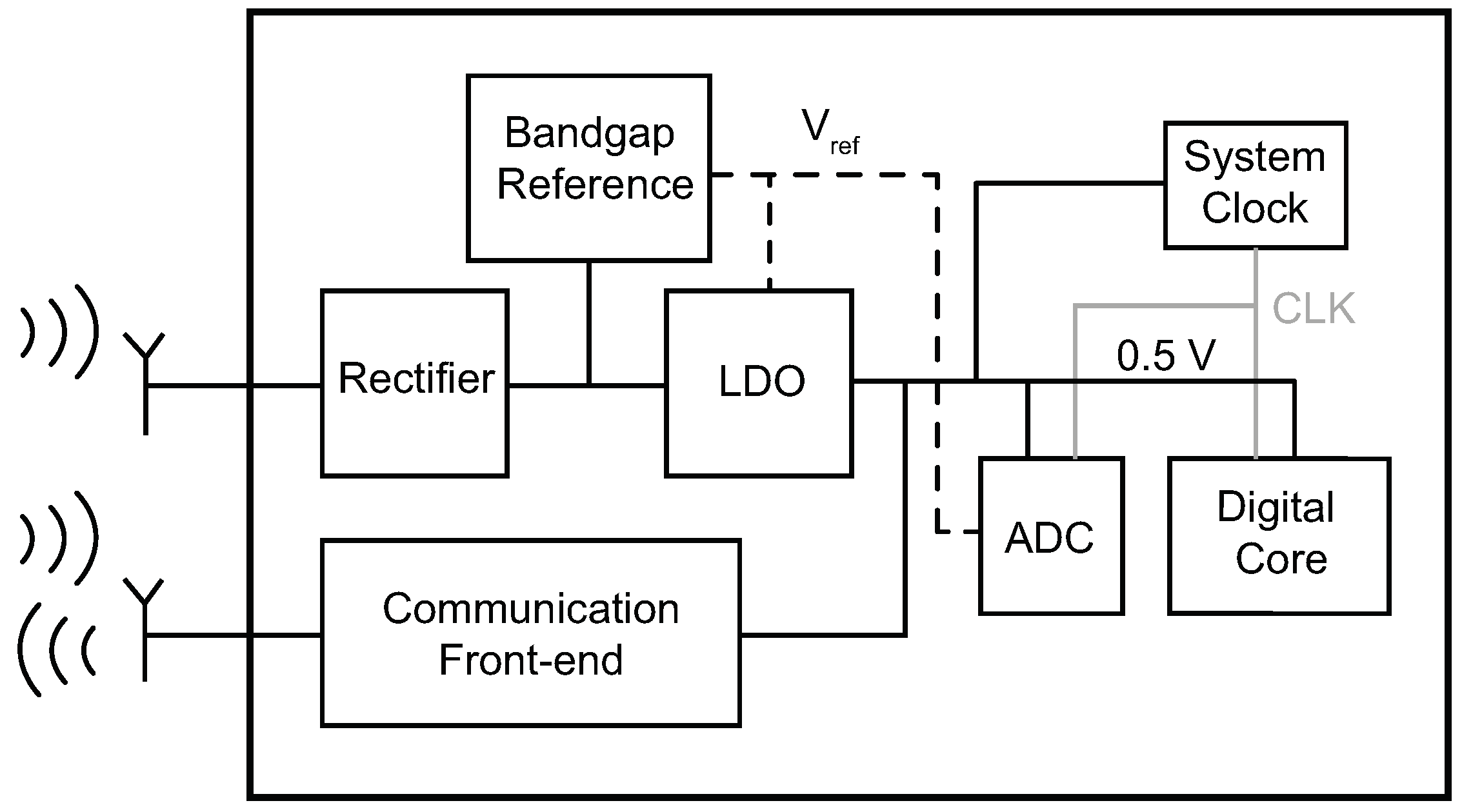
:1. Introduction
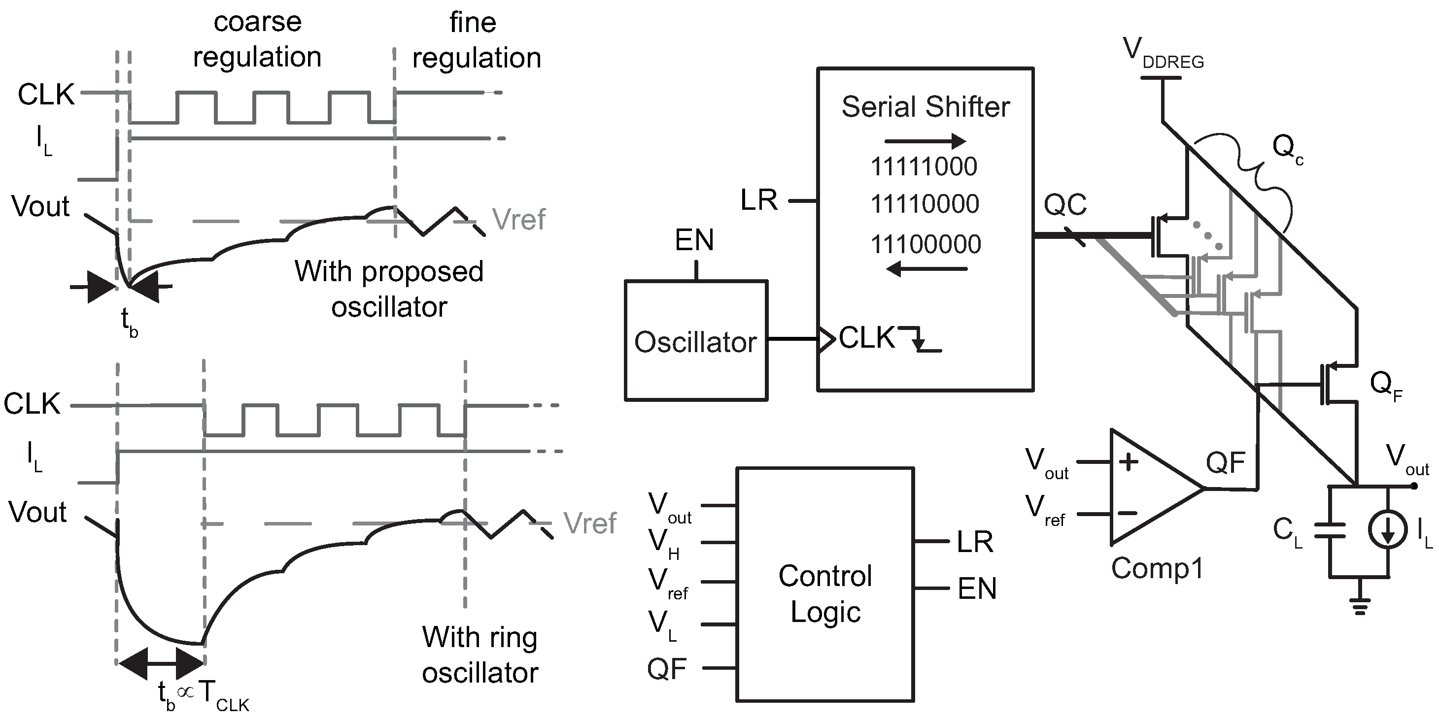
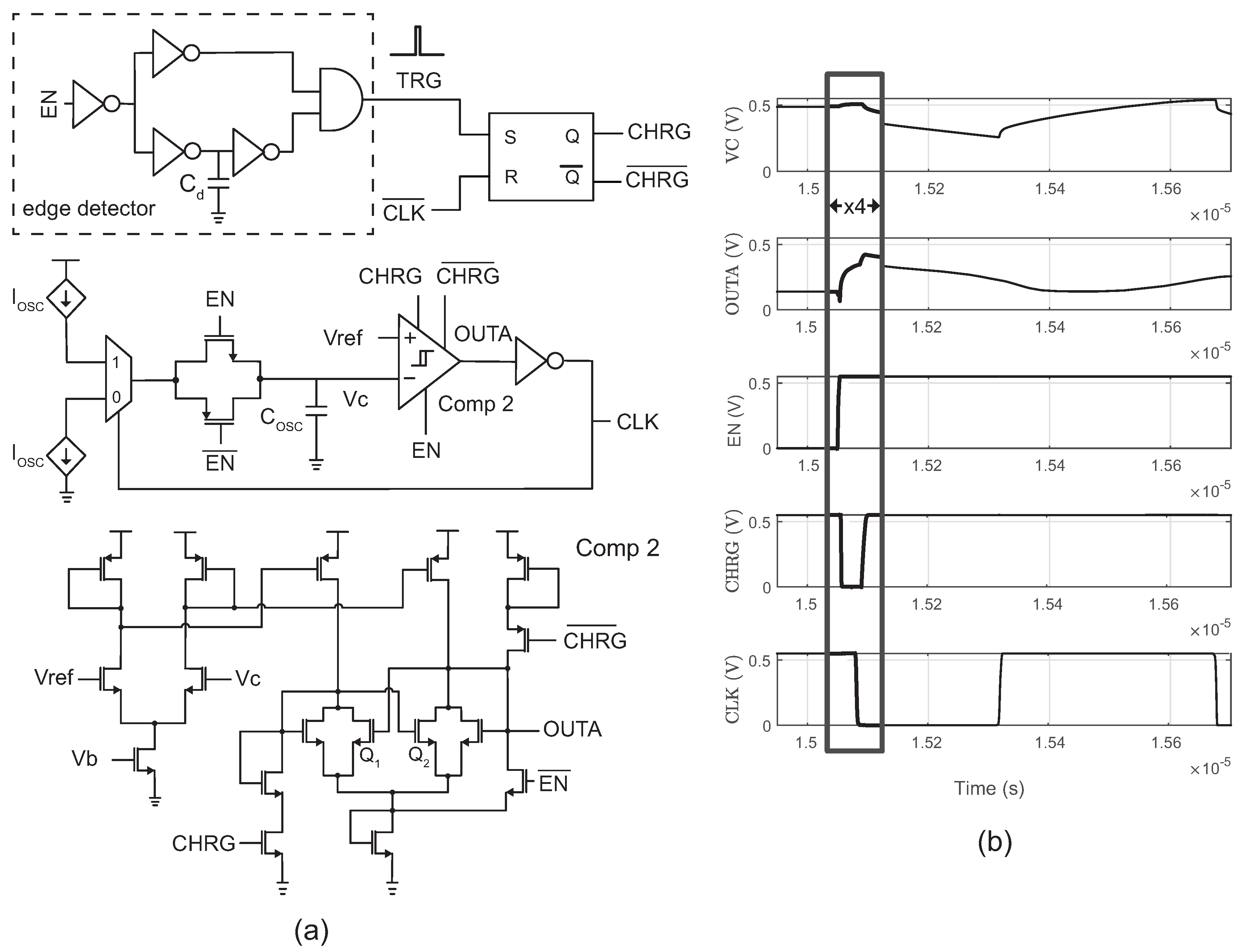
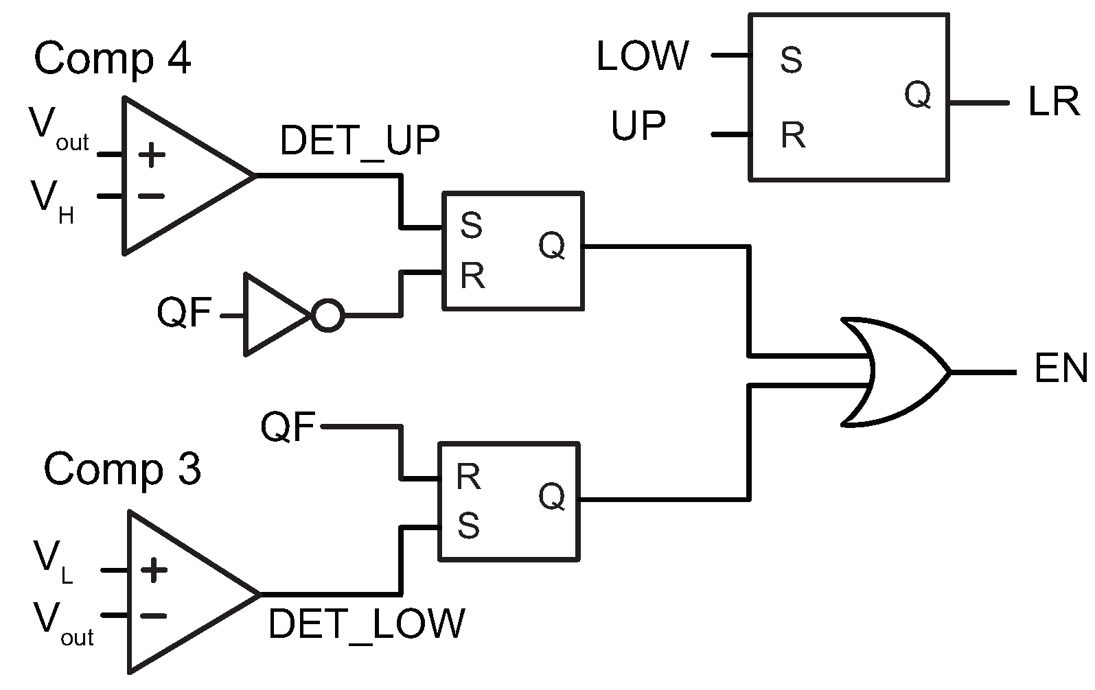
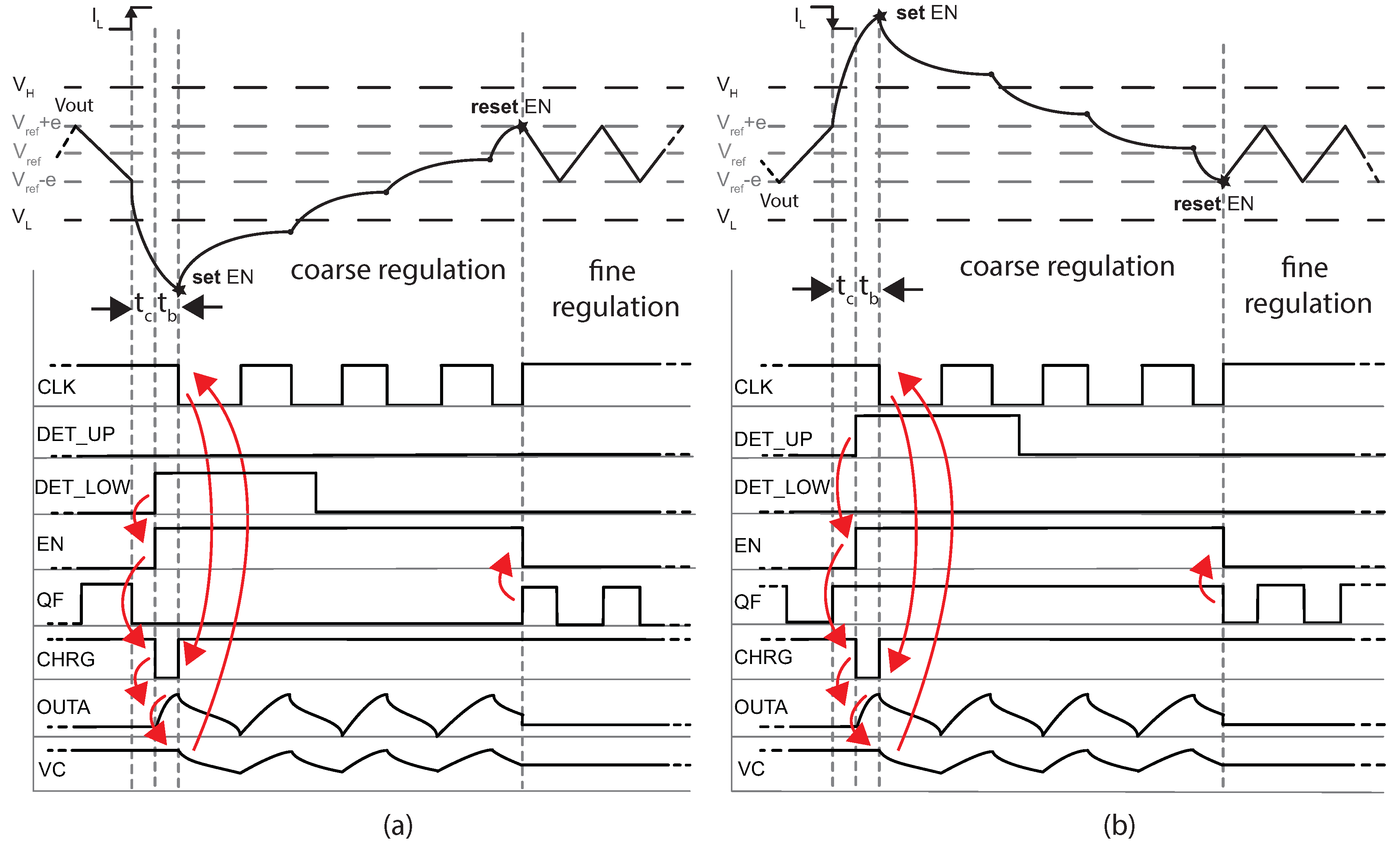
2. Proposed Architecture
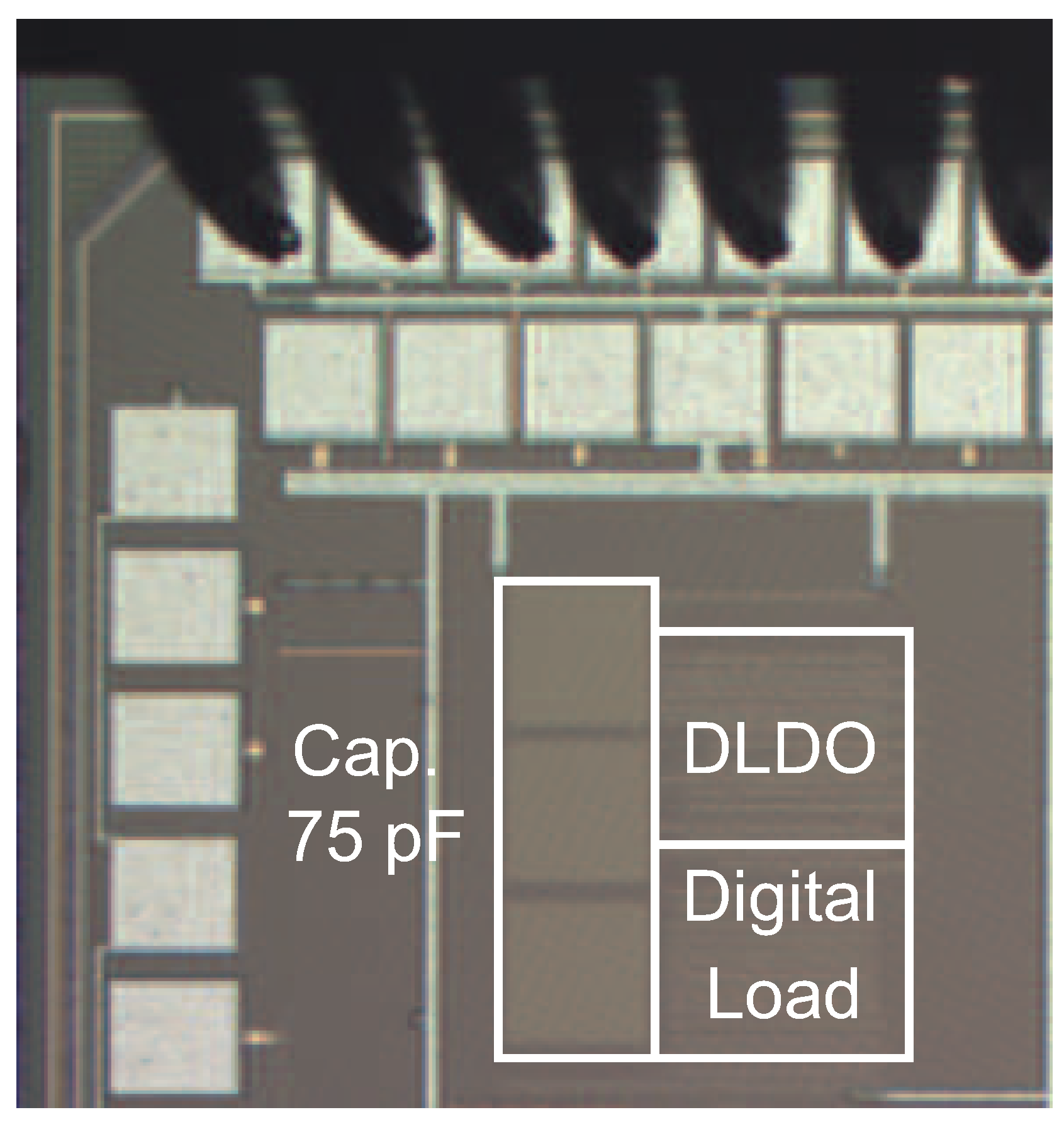
3. Implementation and Methodology
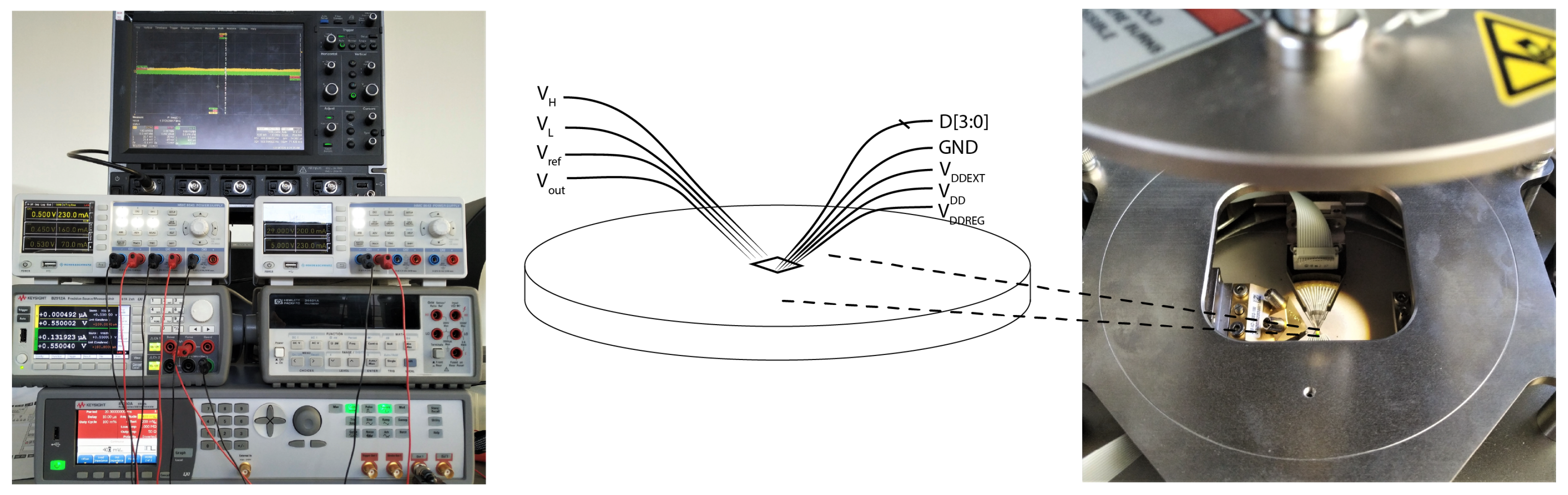
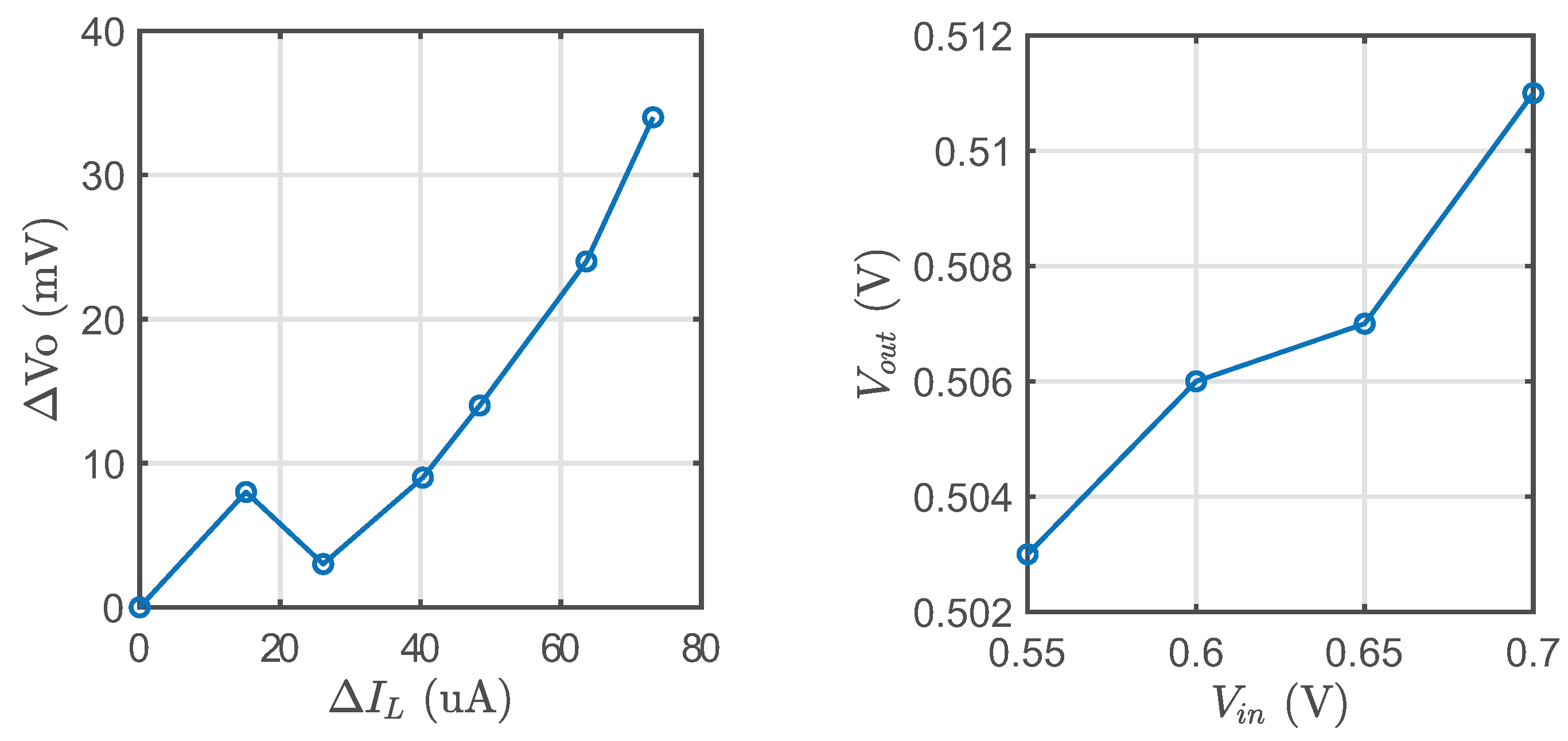
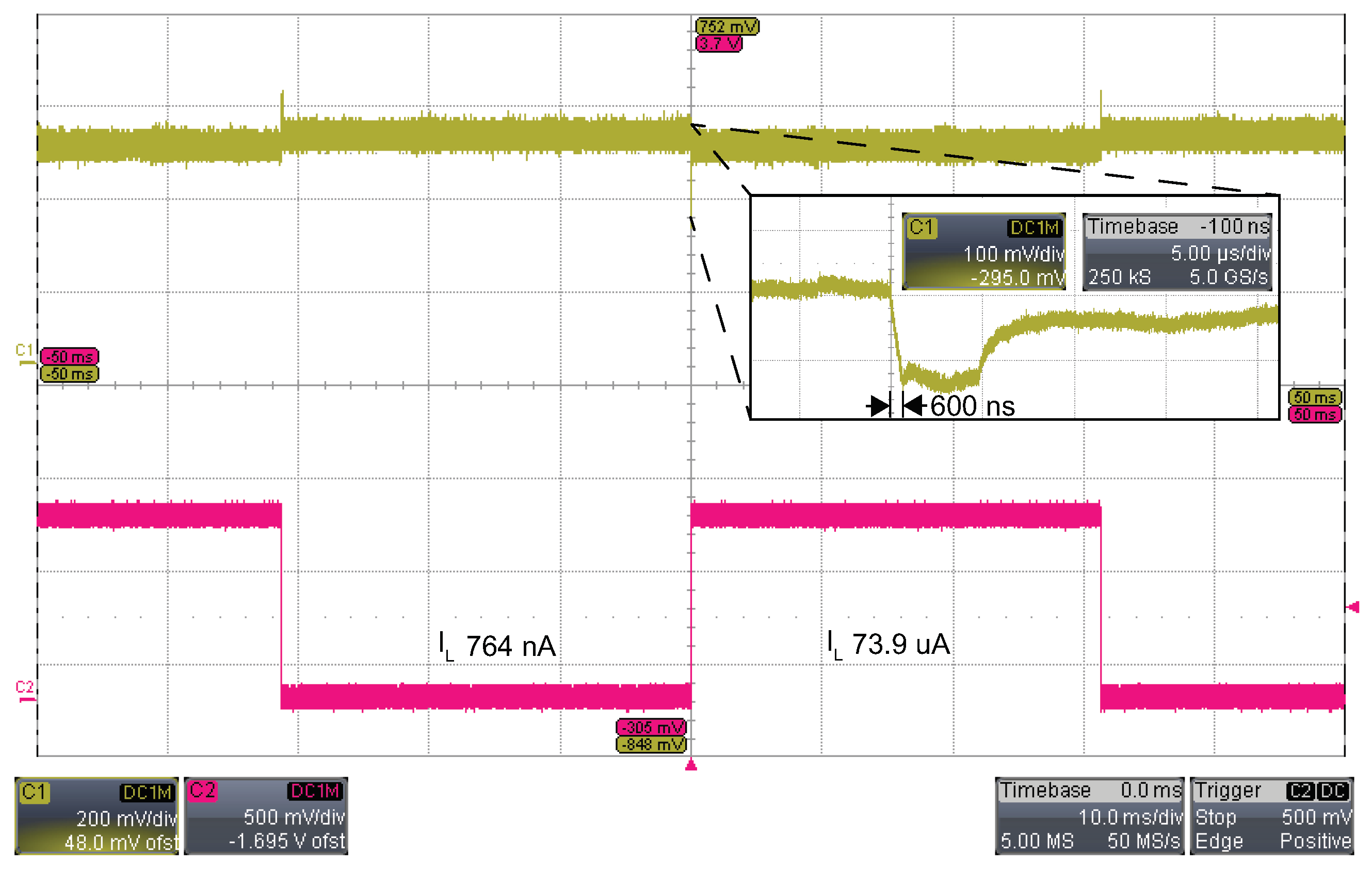
4. Measurements Results
5. Conclusions
Author Contributions
Funding
Acknowledgments
Conflicts of Interest
References
- Yahya, F.B.; Lukas, C.J.; Calhoun, B.H. A Top-Down Approach to Building Battery-Less Self-Powered Systems for the Internet-of-Things. J. Low Power Electron. Appl. 2018, 8, 21. [Google Scholar]
- Chua, A.; Maestro, R.J.; Jardin, J.C.; Monisit, K.; Nuestro, R.; Fabay, K.B.; Pelayo, B.R.; Lofamia, W.V.; Ortiz, J.R.; Madamba, J.A.; et al. Smart-wire: A 0.5 V 44 μW 0 °C to 100 °C power-line energy harvesting sensor node. In Proceedings of the 2017 IEEE Custom Integrated Circuits Conference (CICC), Austin, TX, USA, 30 April–3 May 2017; pp. 1–4. [Google Scholar] [CrossRef]
- Zangi, U.; Feldman, N.; Hadas, T.; Dayag, N.; Shor, J.; Fish, A. 0.45 v and 18 μA/MHz MCU SOC with Advanced Adaptive Dynamic Voltage Control (ADVC). J. Low Power Electron. Appl. 2018, 8, 14. [Google Scholar] [CrossRef] [Green Version]
- Quelen, A.; Badets, F.; Pillonnet, G. A sub-100 nW power supply unit embedding untrimmed timing and voltage references for duty-cycled μW-range load in FDSOI 28 nm. In Proceedings of the ESSCIRC 2017—43rd IEEE European Solid State Circuits Conference, Leuven, Belgium, 11–14 September 2017; pp. 279–282. [Google Scholar]
- Mu, J.; Liu, L.; Zhu, Z.; Yang, Y. A 58-ppm/°C 40-nW BGR at Supply From 0.5 V for Energy Harvesting IoT Devices. IEEE Trans. Circuits Syst. II Express Briefs 2017, 64, 752–756. [Google Scholar] [CrossRef]
- Mu, J.; Liu, L.; Zhu, Z.; Yang, Y. A 0.5 V, 40 nW voltage reference for WBAN devices. In Proceedings of the 2016 IEEE Biomedical Circuits and Systems Conference (BioCAS), Shanghai, China, 17–19 October 2016; pp. 504–507. [Google Scholar] [CrossRef]
- Shrivastava, A.; Craig, K.; Roberts, N.E.; Wentzloff, D.D.; Calhoun, B.H. 5.4 A 32 nW bandgap reference voltage operational from 0.5 V supply for ultra-low power systems. In Proceedings of the 2015 IEEE International Solid-State Circuits Conference—(ISSCC) Digest of Technical Papers, San Francisco, CA, USA, 22–26 February 2015; pp. 1–3. [Google Scholar] [CrossRef]
- Lahiri, A.; Badrathwal, P.; Jain, N.; Chatterjee, K. A 0.5 V supply, 49 nW band-gap reference and crystal oscillator in 40 nm CMOS. In Proceedings of the 2017 IEEE Custom Integrated Circuits Conference (CICC), Austin, TX, USA, 30 April–3 May 2017; pp. 1–4. [Google Scholar] [CrossRef]
- Ahmed, K.Z.; Krishnamurthy, H.K.; Augustine, C.; Liu, X.; Weng, S.; Ravichandran, K.; Tschanz, J.W.; De, V. A Variation-Adaptive Integrated Computational Digital LDO in 22-nm CMOS With Fast Transient Response. IEEE J. Solid State Circuits 2020, 55, 977–987. [Google Scholar] [CrossRef]
- Salem, L.G.; Warchall, J.; Mercier, P.P. A Successive Approximation Recursive Digital Low-Dropout Voltage Regulator with PD Compensation and Sub-LSB Duty Control. IEEE J. Solid State Circuits 2018, 53, 35–49. [Google Scholar] [CrossRef]
- Otsuga, K.; Onouchi, M.; Igarashi, Y.; Ikeya, T.; Morita, S.; Ishibashi, K.; Yanagisawa, K. An on-chip 250 mA 40 nm CMOS digital LDO using dynamic sampling clock frequency scaling with offset-free TDC-based voltage sensor. In Proceedings of the 2012 IEEE International SOC Conference, Niagara Falls, NY, USA, 25–28 September 2012; pp. 11–14. [Google Scholar]
- Lee, Y.H.; Peng, S.Y.; Chiu, C.C.; Wu, A.C.H.; Chen, K.H.; Lin, Y.H.; Wang, S.-W.; Tsai, T.-Y.; Huang, C.-C.; Lee, C.C. A Low Quiescent Current Asynchronous Digital-LDO With PLL-Modulated Fast-DVS Power Management in 40 nm SoC for MIPS Performance Improvement. IEEE J. Solid State Circuits 2013, 48, 1018–1030. [Google Scholar] [CrossRef]
- Nasir, S.B.; Gangopadhyay, S.; Raychowdhury, A. All-digital low-dropout regulator with adaptive control and reduced dynamic stability for digital load circuits. IEEE Trans. Power Electron. 2016, 31, 8293–8302. [Google Scholar] [CrossRef]
- Kim, D.; Kim, S.; Seok, M.; Ham, H.; Kim, J. 0.5 V—Vin, 165-mA/mm2 fully-integrated digital LDO based on event-driven self-triggering control. In Proceedings of the 2018 IEEE Symposium on VLSI Circuits, Madurai, India, 28–30 June 2018; pp. 109–110. [Google Scholar]
- Li, S.; Calhoun, B.H. 14.6 a 745 pA hybrid asynchronous binary-searching and synchronous linear-searching digital ldo with 3.8 105 dynamic load range, 99.99% current efficiency, and 2 mV output voltage ripple. In Proceedings of the 2019 IEEE International Solid- State Circuits Conference—(ISSCC), San Francisco, CA, USA, 17–21 February 2019; pp. 232–234. [Google Scholar]
- Bose, S.; Johnston, M.L. A Stacked-Inverter Ring Oscillator for 50 mV Fully-Integrated Cold-Start of Energy Harvesters. In Proceedings of the 2018 IEEE International Symposium on Circuits and Systems (ISCAS), Florence, Italy, 27–30 May 2018; pp. 1–5. [Google Scholar]
- Saito, T.; Komatsu, S. A low—Voltage hysteresis comparator for low power applications. In Proceedings of the 2017 24th IEEE International Conference on Electronics, Circuits and Systems (ICECS), Batumi, GA, USA, 5–8 December 2017; pp. 427–430. [Google Scholar]


| [10] | [9] | [13] | [15] | [14] | This Work | |
|---|---|---|---|---|---|---|
| Process | 65 | 22 | 130 | 65 | 65 | 55 |
| Control | PD | DVFS | ASF | ABS/SLS | ED PI | ED NLC |
| Oscillator | W/O | W/O | INT. | INT. | INT. | INT. |
| Active Area [] | 0.0023 | 0.165 | 0.114 | 0.048 | 0.0057 | 0.035 |
| Vin [V] | 0.5–1 | 0.55–1.2 | 0.5–1.2 | 0.5–1 | 0.45–1 | 0.55–0.7 |
| Vout [V] | 0.3–0.45 | 0.5–1.15 | 0.45–1.14 | 0.4–0.95 | 0.4–0.95 | 0.5 |
| Range | 100 – 2 | 400 – 2 | 100 – 4.6 | 710 pA– 0.27 | 15 – 5.6 | 0.5 – 80 |
| [] | 0.4 | 7 | 1 ext. | 100 ext. | 0.1 | 0.075 |
| 14 | 2.4 | 20–751 | 745 | 18.1 | 0.56 | |
| Ripple [] | N/R | N/R | 10–70 | 2 | N/R | 40–50 |
| Settling. time, Tr. test | 100 | N/R | N/R | 48 | 1 | 20 |
| @, Tr. test | 40 @ 1.06 | 100 @ 0.5 | 40 @ 0.7 | 76.5 @ 0.27 | 49.8 @ 2.3 | 150 @ 73 |
| Load step, Tr. test | <1 | 250 | N/R | 500 ns | 0.1 | 4 |
| FOM [], Tr. test | 0.469 | 9.3 * | 4.3 * | 0.049 | 0.086 | 0.175 |
Publisher’s Note: MDPI stays neutral with regard to jurisdictional claims in published maps and institutional affiliations. |
© 2020 by the authors. Licensee MDPI, Basel, Switzerland. This article is an open access article distributed under the terms and conditions of the Creative Commons Attribution (CC BY) license (http://creativecommons.org/licenses/by/4.0/).
Share and Cite
Konstantopoulos, C.; Ussmueller, T. A Nano-Power 0.5 V Event-Driven Digital-LDO with Fast Start-Up Burst Oscillator for SoC-IoT. J. Low Power Electron. Appl. 2020, 10, 41. https://0-doi-org.brum.beds.ac.uk/10.3390/jlpea10040041
Konstantopoulos C, Ussmueller T. A Nano-Power 0.5 V Event-Driven Digital-LDO with Fast Start-Up Burst Oscillator for SoC-IoT. Journal of Low Power Electronics and Applications. 2020; 10(4):41. https://0-doi-org.brum.beds.ac.uk/10.3390/jlpea10040041
Chicago/Turabian StyleKonstantopoulos, Christos, and Thomas Ussmueller. 2020. "A Nano-Power 0.5 V Event-Driven Digital-LDO with Fast Start-Up Burst Oscillator for SoC-IoT" Journal of Low Power Electronics and Applications 10, no. 4: 41. https://0-doi-org.brum.beds.ac.uk/10.3390/jlpea10040041