CMOS Inverter as Analog Circuit: An Overview


1
Department of Electrical Engineering and Computer Sciences, University of California at Berkeley, Berkeley, CA 94720, USA
2
Ayar Labs, Santa Clara, CA 95054, USA
J. Low Power Electron. Appl. 2019, 9(3), 26; https://0-doi-org.brum.beds.ac.uk/10.3390/jlpea9030026
Submission received: 24 June 2019
/
Revised: 19 July 2019
/
Accepted: 17 August 2019
/
Published: 20 August 2019
Abstract
:Since the CMOS technology scaling has focused on improving digital circuit, the design of conventional analog circuits has become more and more difficult. To overcome this challenge, there have been a lot of efforts to replace conventional analog circuits with digital implementations. Among those approaches, this paper gives an overview of the latest achievement on utilizing a CMOS inverter as an analog circuit. Analog designers have found that a simple resistive feedback pulls a CMOS inverter into an optimum biasing for analog operation. Recently developed applications of the resistive-feedback inverter, including CMOS inverter as amplifier, high-speed buffer, and output driver for high-speed link, are introduced and discussed in this paper.
1. Introduction
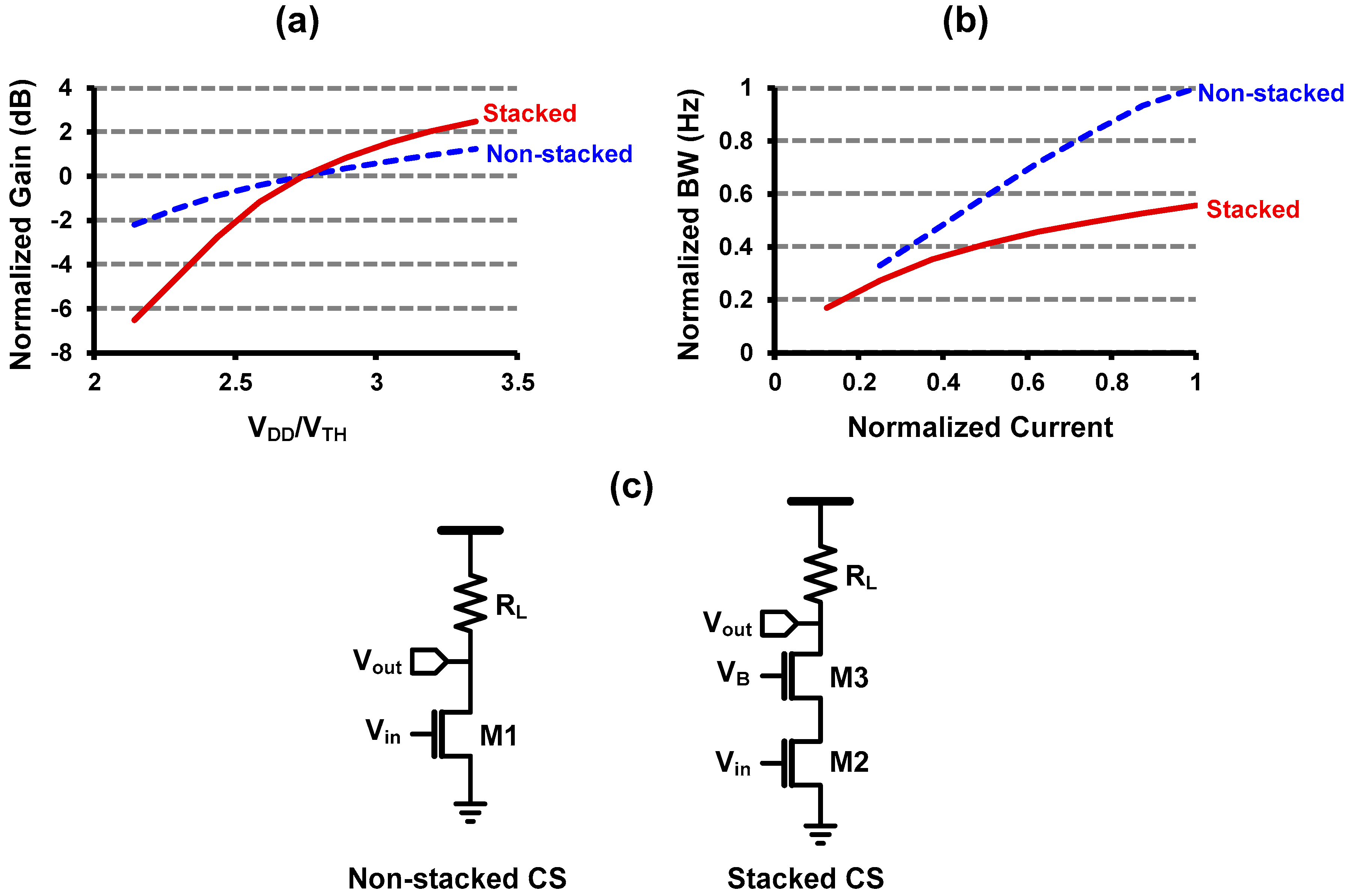
Since the 1960s, scaling of silicon technologies (Moore’s law) has dominantly driven the semiconductor industry, as the scaling is actually the almighty knob for all the challenges we have had; lower power consumption, higher speed, and higher density. However, the main focus of the scaling has been the improvement of digital circuit, for example high Ion/Ioff ratio, as the computing capability has been constrained by the power consumption, instead of the speed of the transistor [1,2]. Such digital-driven scaling leads to several issues in analog circuit design. For instance, the intrinsic gain of transistor has been significantly reduced due to the short-channel effect. Moreover, the threshold voltage of transistor has not been scaled at the same rate of the supply voltage scaling, in order for suppressing the leakage current [3]. That means the “normalized” voltage headroom for analog circuit has been reduced. Therefore, adopting conventional gain-boosting techniques (i.e., cascode) becomes more and more difficult in modern CMOS technology [4]. What makes things worse is that the gate-overdrive voltage of analog circuits should be decreased as the voltage headroom reduces, which increases the sensitivity of analog circuits to the device mismatch [5]. We can observe such trend in Figure 1, which compares the stacked common-source (CS) amplifier to the non-stacked CS amplifier [6,7]. Figure 1a,b shows the normalized gain of CS amplifiers with respect to VDD/VTH and the normalized large-signal bandwidth with respect to the normalized current dissipation, respectively. The gain of the stacked topology decreases much steeper than that of the non-stacked, which means that the gain enhancement from the cascode topology becomes less attractive in the modern CMOS technology where the voltage headroom is reduced. Moreover, the achievable bandwidth of the stacked amplifier is much less than the non-stacked amplifier even when it dissipates more current, because the increased self-loading from the stacked transistor degrades the rise/fall time. In addition, [6] revealed that the input-referred noise becomes even worse in the stacked topology because the transconductance gm increases due to the reduced gate-overdrive voltage.
In summary, what we could observe from the CMOS scaling trend is that the scaling has focused on improving the digital circuits; hence, the performance of analog circuits has been degraded due to the short-channel effect and the reduced voltage headroom. The analog circuit designers have come up with the fact that a CMOS inverter, which is the representative of the digital circuit family, can be the most powerful circuit in modern CMOS technologies, even in the analog domain [8,9]. First, there is no stacking; thus, it has not been affected by the reduced voltage headroom. Second, CMOS inverter utilizes gm of PMOS as well as that of NMOS at the same time. When we compare the two circuits given in Figure 2, we can find that they have the same load capacitance, including the self-loading. However, in case of the CMOS inverter, the overall gm is the sum of gmN and gmP; thus, we can get a higher bandwidth. This aspect becomes much powerful in recent process technologies, where strained silicon technique enhances the PMOS current density as much as that of NMOS [10,11,12]. In fact, when we consider the sizing, the P/N ratio of the inverter for analog intent is different to the digital intent. In order technology where the strained silicon technique is not adopted, digital inverter has PMOS which is generally twice larger than NMOS, because we have to match the strength of PMOS and NMOS, since we assume that only one of the PMOS and NMOS is turned on at a time. However, in such analog inverter, the optimum is at around P/N ratio of unity, where we can achieve the highest gm per input capacitance [13]. Note that the PMOS and NMOS continuously run together in analog mode. That means we were not able to fully utilize the gmP in older technology nodes. In other words, the strained silicon boosts the current density of PMOS to be matched to that of NMOS, and therefore it makes the analog inverter become more powerful.
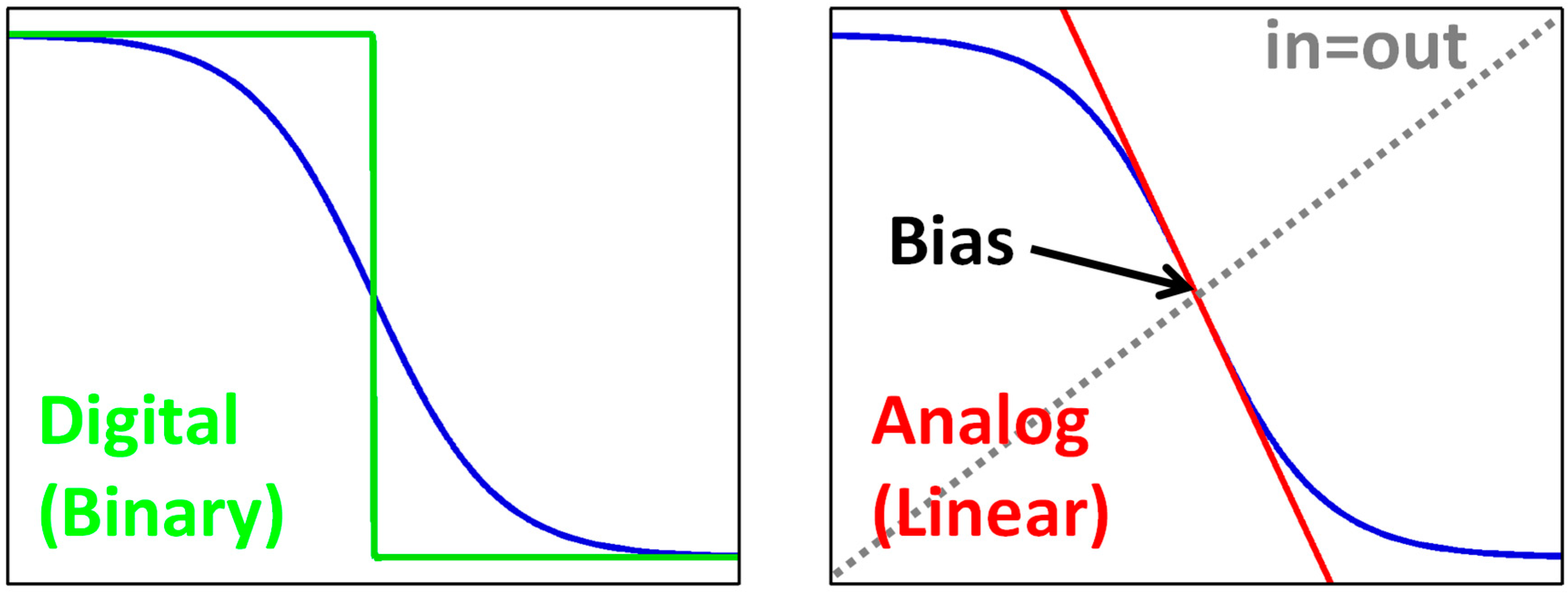
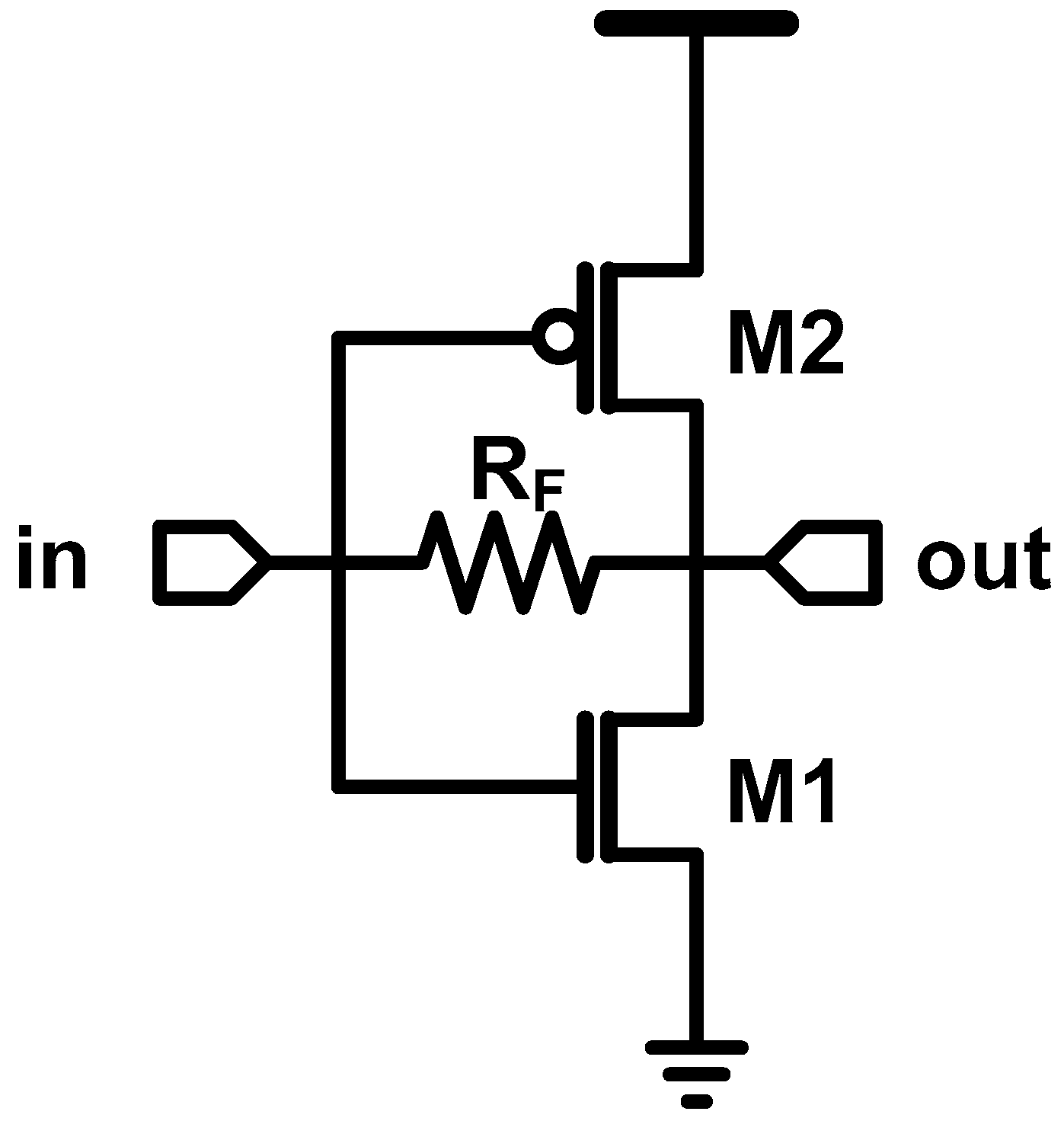
Some readers may wonder how a CMOS inverter acts like an analog circuit, because it is a representative digital circuit. In fact, the boundary of analog and digital is ambiguous, but “biasing” can be used to distinguish them, which is explained in Figure 3. The blue line shows the input-output transfer curve of an inverter. Note that the blue lines are the same for both figures. When we see the big picture (large signal), we can find a digital circuit. However, when we focus on a certain operating point (small signal), we can find an analog circuit. We can also find that the maximum gain is achieved at the point where the input and output are the same, that is, at the switching threshold. Analog designers found that such optimum bias point can be achieved with the self-biasing using the resistive feedback, as shown in Figure 4.
Nowadays, in order to take advantage of the CMOS inverter in modern process technology, there has been a lot of approaches to adopt CMOS inverter into analog circuits. This paper focuses on the applications of high-speed analog circuits, and introduces three examples of that, amplifier in optical communication receivers [6,14,15,16,17,18,19,20,21,22,23,24,25,26,27,28,29,30], high-speed clock and data buffer [13,31,32,33,34,35,36,37,38,39,40,41], and output driver for high-speed I/O transmitter [13,40,42,43,44,45,46,47,48,49,50].
2. CMOS Inverter as an Amplifier
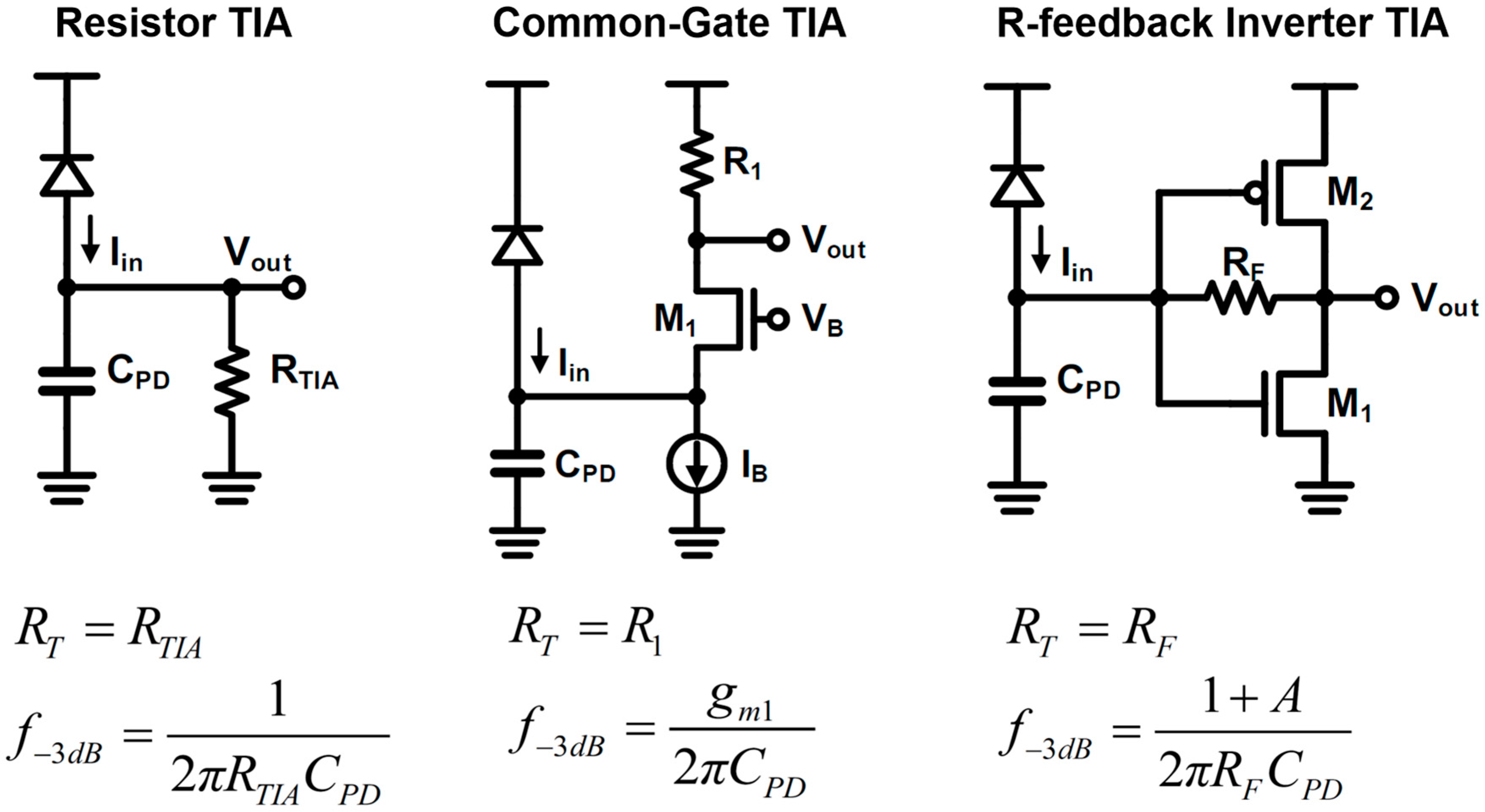
The first example we are going to cover is the use of a CMOS inverter as a high-speed amplifier, which is mostly adopted in optical communication receiver. In optical communication, high-speed serial data is transmitted by modulating the amplitude of light. At the receiving side, a photodetector (PD) converts the received light signal to the photocurrent. Due to the limited PD responsibility as well as and the limited extinction ratio at the transmit side, typically, the amplitude of photo-current signal ranges from tens of uA to hundreds of uA. In order to be processed in a CMOS integrated circuit (IC), the current-mode signal should be converted to voltage-mode. Thus, a trans-impedance amplifier is used at the very front-end of an optical receiver. As a result, the overall performance of the receiver is predominantly determined by the trans-impedance amplifier (TIA). Since there is an inherent trade-off between TIA gain/noise and bandwidth, compound semiconductor process was traditionally preferred to build the optical interface IC due to their high-speed characteristic. However, since continuous advance of CMOS technology has reduced the gap, nowadays, CMOS technology is becoming the mainstream for optical interface ICs.
We can see a brief history of CMOS TIA for optical receiver in Figure 5. The most primitive TIA is a resistor. But there is a strict trade-off between gain and bandwidth, because the gain equals the resistance R and the bandwidth is 1/2πRCPD. In addition, the signal-to-noise (SNR) is another main issue of concern. The total integrated noise due to the thermal noise of the resistor is given as to:
where k is the Boltzmann constant and T is the absolute temperature. Then, the input-referred noise is obtained by dividing (1) with the trans-impedance gain R as:
From (2) we can obtain the SNR to:
where we can observe that higher gain leads to a better SNR, which implies the trade-off of gain/noise over the bandwidth. Many circuit designers have tried to find a way to break the trade-off, and they found that the common-gate (CG) amplifier can break the trade-off. Because the photo-current directly flows to the load resistor, the trans-impedance gain equals to the resistance. On the other hand, the input impedance of the CG amplifier is 1/gm, so the pole at the input of CG amplifier is given as to:
Note that there is no R term in, which implies that the aforementioned trade-off is now broken, since CPD is generally much larger than the load capacitance of the CG amplifier. Since the 1/gm can be reduced by drawing more current by the current source (IB), we can achieve high gain as well as high bandwidth at the cost of power consumption. In addition, [51,52] proposed a regulated-cascode (RGC) TIA, which further improves the gain-bandwidth product of TIA. However, the effectiveness of such stacked configuration has been degraded due to the aforementioned scaling issue, now many researchers have ended up with the resistive feedback inverter TIA. The inverter-TIA still have a similar trade-off as the passive TIA; however, the input resistance of the resistive feedback inverter is R/(1 + A), where A is the gain of the inverter. That means that the trade-off is relaxed by the factor of A. Additionally, note that there is no other path that the photo-current can flow; the gain of this TIA equals R. Readers may consult [28] for a detailed history of TIA evolution.
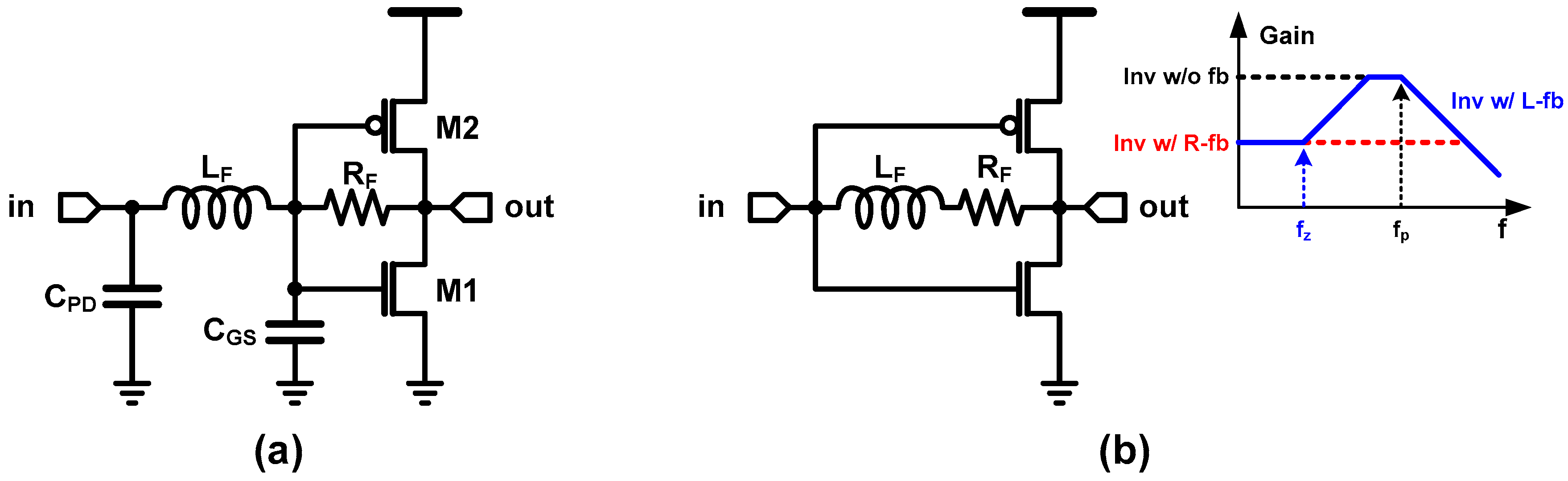
The resistive-feedback inverter TIA is also able to be combined with inductive peaking technique, to extend the bandwidth with less gain/power penalty. References [19,25] present the inverter TIA with series inductive peaking, which is illustrated in Figure 6a. Since an inductor blocks an instantaneous current flow, it enables sequential charging (or discharging) of the two adjacent capacitances (for example, PD capacitance and self-load at the input node, or self-load and load capacitances at the output node), which leads to a faster transient response. On the other hand, [6] added an inductor in series with the feedback resistor; that is, the inductive feedback as shown in Figure 6b. At a low frequency, the effect of the inductor is negligible; thus, the TIA simply follows the transfer gain of the resistive-feedback inverter. Note that such negative feedback increases the bandwidth at the cost of reduced low-frequency gain. On the other hand, the impedance of the inductor increases as the frequency increases; hence, after zero frequency, it surpasses that of the feedback resistor. That means that the total impedance in the feedback path increases, and thus the gain increases. If the inductive impedance is larger enough than the resistance, the transfer gain of the TIA follows that of the inverter without resistive feedback. At a very high frequency, the second order pole, which is introduced by the inductor and the capacitance as well as the intrinsic pole of the inverter, let the transfer gain decrease rapidly as the frequency increases. As a result, such inductive feedback leads to a high-frequency peaking, which can be used to compensate the dominant pole by the CPD. Recent state-of-the-arts works in [15,24,29] have combined the series peaking and the inductive feedback, and therefore considerable high-bandwidth at a quite impressive energy efficiency is achieved. Moreover, the authors in [29] saved inductor area by incorporating T-coil inductive peaking.
The application of CMOS inverter as an amplifier is not limited to the TIA. Optical receivers presented in [18,19,21,24,25,26,27] extend the usage of the CMOS inverter to the post limiting amplifier which follows the TIA. In addition, [16,17,30] present resistive-feedback-inverter-based low-noise amplifier (LNA) and variable gain amplifier (VGA), respectively. In such applications, a normal inverter stage and a resistive-feedback stage are placed alternately to retain the self-bias (resistive feedback) as well as high gain (inverter), as shown in Figure 7. Recalling Figure 3, the small-signal gain of inverter is maximized at the crossover voltage. Therefore, in order to maximize the overall gain of the amplifier chain, the common-mode voltage should be corrected. Due to the considerably large gain of the chain, the resistive feedback itself is not enough to retain a correct bias point. Such common-mode variation leads to some large-signal non-idealities, such as duty-cycle distortion. Therefore, a common-mode feedback is generally included as shown in the example of Figure 7. The DC component of the output signal is extracted through a low-pass filter (LPF) and then compared to the reference voltage (i.e., crossover voltage). The feedback adjusts the input common level until the common-mode voltage at the output becomes the same as the reference voltage.
To sum up, the resistive-feedback inverter has become a mainstream of TIA implementation, to fully utilize the CMOS process scaling, against the conventional TIA structures. Moreover, there have been many efforts to extend the application to other high-speed amplifiers. For evidence, taking advantage of the advanced CMOS technology node (14 nm FinFet), [25], where the inverter-based TIA and post amplifier are adopted, achieves the highest bandwidth optical receiver, which achieves 64 Gb/s with binary signaling.
3. High Speed Buffer
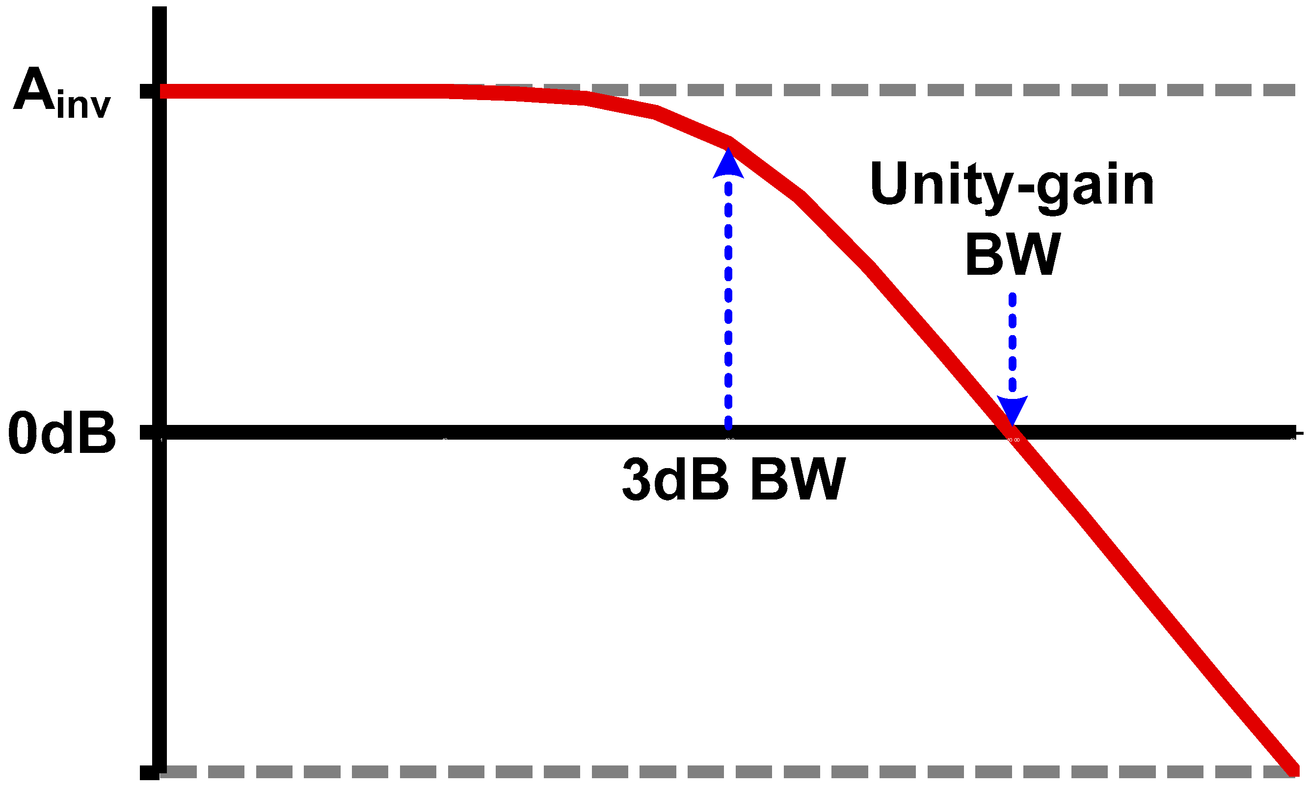
In the previous section, we focused on the small-signal behavior of CMOS inverter (with resistive feedback). Here, we will be care of more large-signal-like behavior compared to the amplifier operation. If the input signal swing is large enough, that is, entering to the noise margin region, the amplitude of the signal no longer needs to be considered as long as the gain of the “buffer” is larger than unity. However, taking into account the intrinsic gain of an inverter, the 3 dB bandwidth is typically 5–10× lower than the unity-gain bandwidth (Figure 8). If the main signal component is at between the 3 dB bandwidth and the unity-gain bandwidth, the signal experiences distortion while passing through the buffer even though the amplitude is not attenuated. For example, since the phase delay is not a constant over the frequency, a pattern-dependent jitter will be introduced to the non-return-to-zero (NRZ) datastream even if the Nyquist frequency is below the unity-gain bandwidth of the buffer [53]. Clock signal is another good and simpler example, as there is only a single frequency tone. Let us take into account additive white noise. The amplitude noise is filtered out by the noise margin of inverter; however, the phase noise propagates through the inverter. Moreover, if the clock frequency is higher than the 3 dB bandwidth, the low frequency noise has a larger gain than the fundamental frequency component. That leads to the jitter amplification [54]. Duty-cycle distortion is another important issue, since the duty-cycle is actually the DC component of the signal so the duty-cycle error is amplified after passing through a band-limited buffer [42].
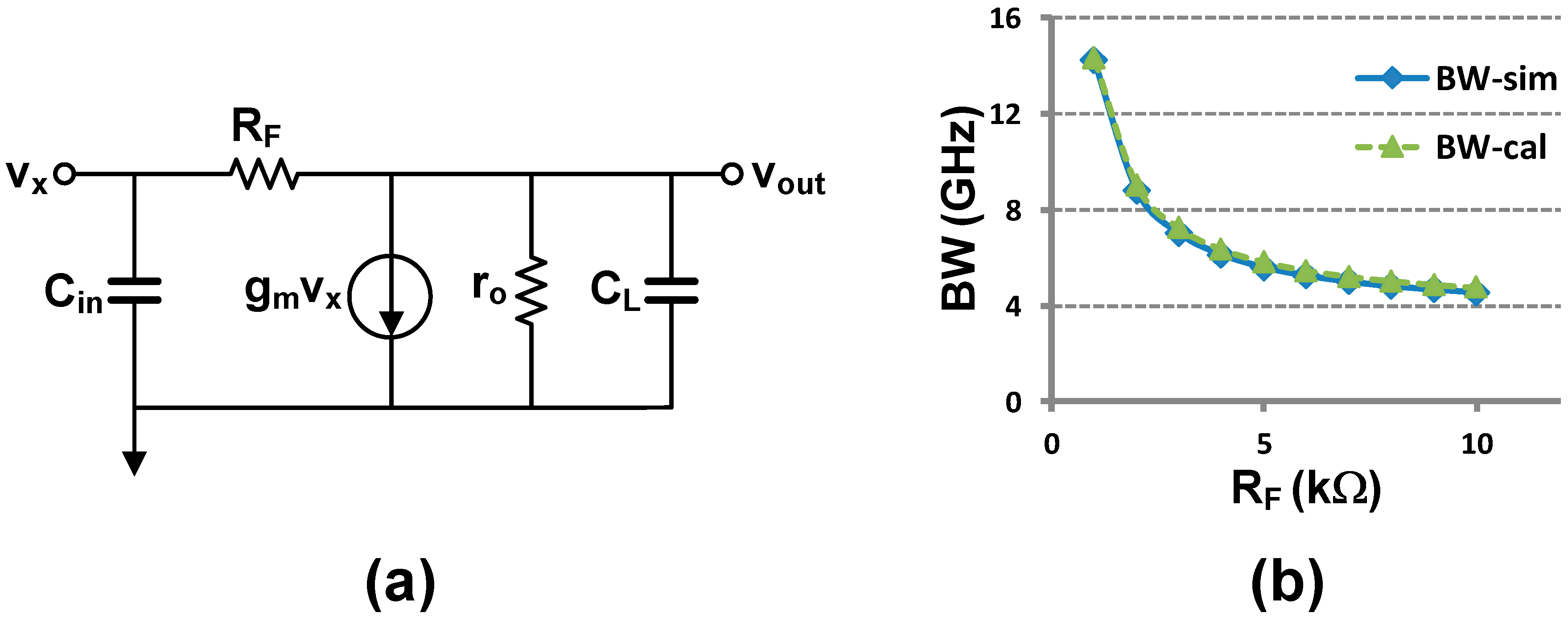
The above observation implies that the 3 dB bandwidth is more important than the unity-gain bandwidth while handling a high-speed analog signal, in contrary to the digital intent. The resistive feedback is also very useful to extend the 3 dB bandwidth of the inverter. We can obtain a quantitative analysis how the resistive feedback extends the bandwidth of the inverter, from the small signal model shown in Figure 9. Applying KCL to the output node, we obtain:
where gm is the sum of gmN and gmP. Equation (5) leads to the transfer function as:
where we can achieve the 3 dB bandwidth to:
Note that the 3 dB bandwidth of the inverter without feedback is 1/roCL. That is, the resistive feedback increases the 3 dB bandwidth by 1/RFCL. Simulated bandwidth shown in Figure 9b verifies (7). Moreover, thanks to the negative feedback, this circuit is less sensitive to the PVT variations compared to the normal CMOS inverter.
On the other hand, an AC-coupling capacitor is widely used at the input of the resistive feedback inverter, for clock buffer application [32,33,34,35,36,37,38,39] (Figure 10). The primary motivations of the AC coupling for the clock buffer are as follows:
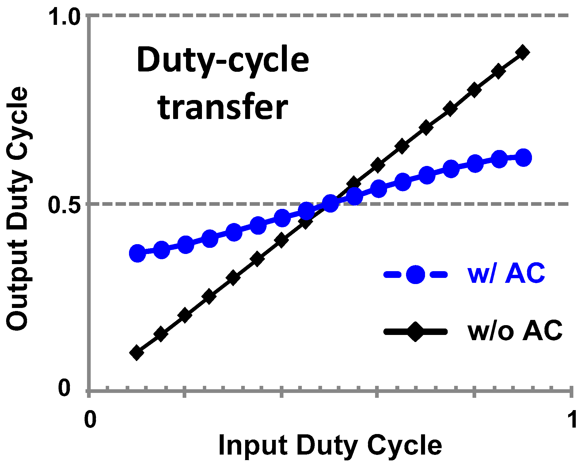
- Since AC coupling completely blocks the DC component of the clock signal, the duty-cycle distortion does not propagate. Thanks to the self-biasing to the cross-over voltage, the duty-cycle is restored to the ideal value regardless of the input duty-cycle (Figure 11).
- Combined with the low-pass characteristic of the inverter, AC coupling results in a band-pass characteristic. Because a band-pass filter attenuates all out-of-band noise, it suppresses phase noise and jitter from the input clock [54].
- Because the clock buffer does not have to deal with a wide-band signal, the high-frequency cut-off frequency can be fairly high (<~1/10 of the clock frequency). Therefore, a small capacitor can be used [39].
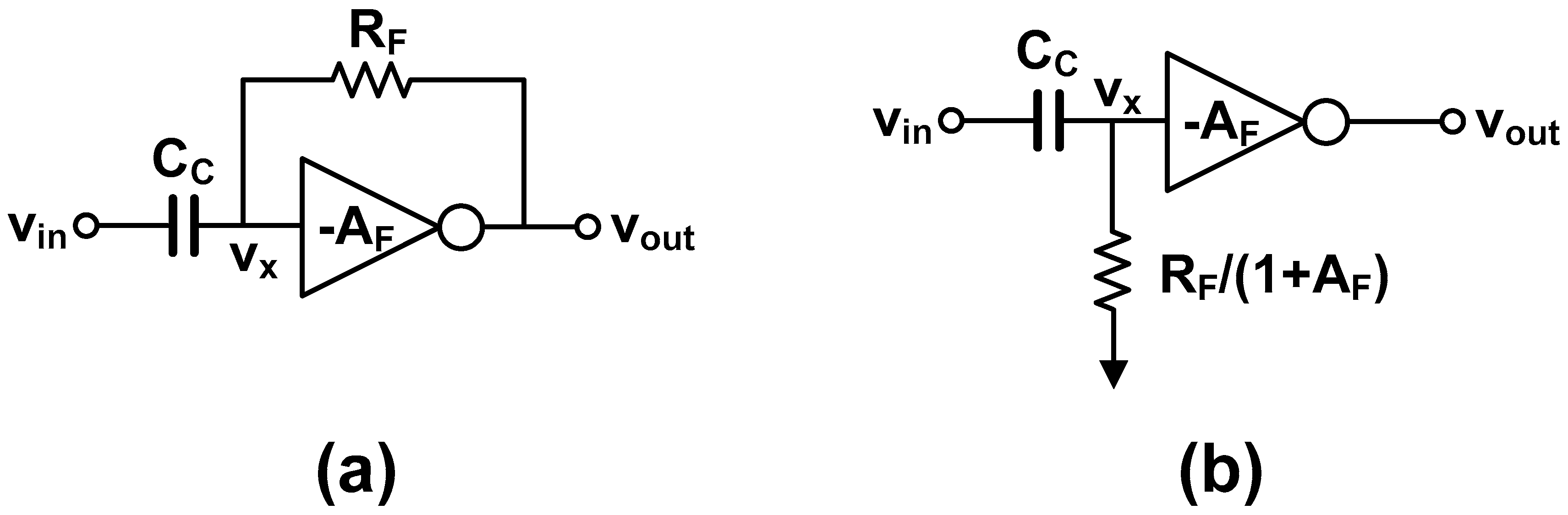
The high-pass cut-off frequency of the AC-coupled buffer is calculated as follows. Using Miller approximation, the feedback resistance RF is translated to the input resistance of RF/(1 + AF), where AF is the DC gain of the inverter. Then, we obtain:
where we can find that the high-pass cut-off frequency is:
For reference, the overall transfer function without Miller approximation is given in [39] as:
where CL is the load capacitance of the buffer. Figure 11 shows an example of the simulated duty-cycle transfer function of an AC-coupled inverter.
On the other hand, the bandwidth dependency on the feedback resistance can also be utilized to control the delay of a buffer chain. Conventionally, a current-starved inverter [55] or a variable capacitive-load inverter [56] have been widely used to build a variable delay line. However, basically, their mechanism is to reduce the bandwidth of CMOS inverter to increase the delay. As a result, such delay cells have a lower bandwidth than an inverter, and therefore, they have usually become the main limiting factor of the maximum speed of a chip. As a remedy, [13,40,41] proposed a resistive-feedback based delay line whose delay is controlled by adjusting the feedback resistance. As we observed in (7) and Figure 9b, the feedback extends the bandwidth of an inverter. That means that the resistive-feedback delay line actually increases the bandwidth to adjust the delay, instead of reducing the bandwidth. From another qualitative viewpoint of large signal, the resistive feedback decreases the voltage swing; therefore, the output rise/fall time is reduced. References [13,40] verified the large-signal effect as well, such that the resistive feedback reduces ISI considerably compared to the conventional delay line, at the cost of increased power consumption due to the short-circuit current induced by the reduced voltage swing.
4. Output Driver for High-Speed Wireline Communication
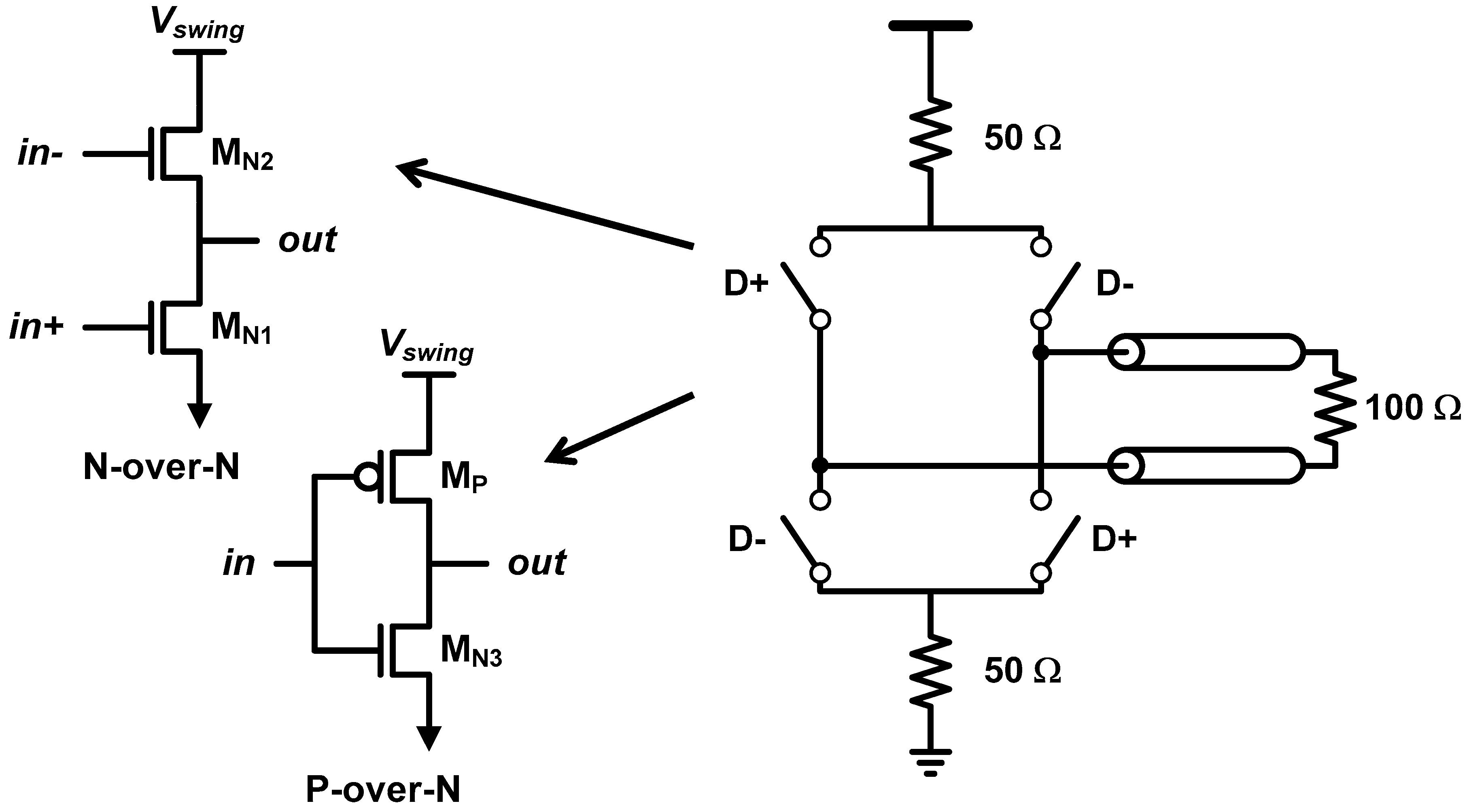
The last example is the output driver for high-speed I/O link. On the right side of Figure 12, we can find a conceptual diagram of a source-series terminated (SST) driver, which is also known as a voltage-mode driver [35,36,37,38,39,40,41,42,43,44,45,46,47,48,49,50]. Instead of relying on a parallel resistance to match the driver’s output impedance with the characteristic impedance of the transmission channel, the SST driver adopts series termination. Such series-terminated data transmission is conceptually enabled with a series combination of a 50-Ω resistance and an ideal switch driven by NRZ data. The main advantage of SST driver over the parallel-termination counterpart, which is represented by current-mode logic (CML) driver, is its low-power consumption. Assuming terminations at both transmit and receive sides (double termination), the series termination flows the signal current to 100-Ω resistance (I = Vswing/100), whereas the parallel termination flows to 25 Ω (I = Vswing/25). As a result, the parallel termination dissipates 4× higher current to achieve a same voltage swing. On the other hand, the main downside of SST driver originates to the fact that there is no ideal switch in IC. There are two types of practical SST implementation, N-over-N and P-over-N configurations, as shown in Figure 12. It is well known that the N-over-N works well only for low swing applications, whereas the P-over-N is appropriate for higher swing applications. Note that the P-over-N structure is a CMOS inverter. Basically, their approach is the same. Instead of using an ideal 0-Ω switch, they utilize the finite resistance of switch transistor; if the turn-on resistance equals to 50-Ω, a single transistor can work as the combination of the ideal switch and the resistor. The 50-Ω impedance is generally calibrated by adjusting the number of activated driver slices and the gate-overdrive voltage. The main challenge here is the non-linear nature of CMOS transistor does not let the transistors have a constant resistance over the swing range [42]. For example, when the output voltage increases, the VDS of the pull-down NMOS (MN1, MN3) increases and causes the NMOS to fall into the saturation region, where the output impedance becomes very high. Note that the linearity is a function of VDS, and the VDS range equals the output swing.
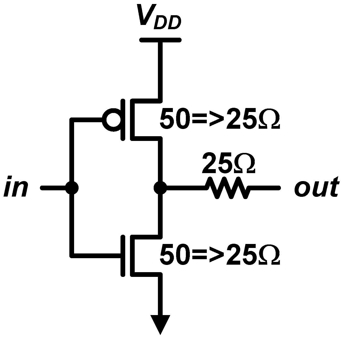
To resolve this issue, a series resistance is placed at the output of the SST driver, as shown in Figure 13 [37,46,47,48]. The turn-on resistance of the transistor is reduced here (i.e., 25 Ω) to make the sum with the series resistance be 50 Ω. The series resistor takes charge of a portion of the output swing, hence, the VDS of the transistors is reduced. The downside of this approach is the increased transistor size. If 25-Ω resistance is used, the size of transistor is doubled so that both the input capacitance and the output self-capacitance are doubled, each of which increases burdens of the pre-driver stage and degrades the bandwidth of the driver itself, respectively. Note that the transistors should operate in the linear region for better linearity, where the current density is much lower than that in the saturation region. Therefore, the device size is generally enormously large.
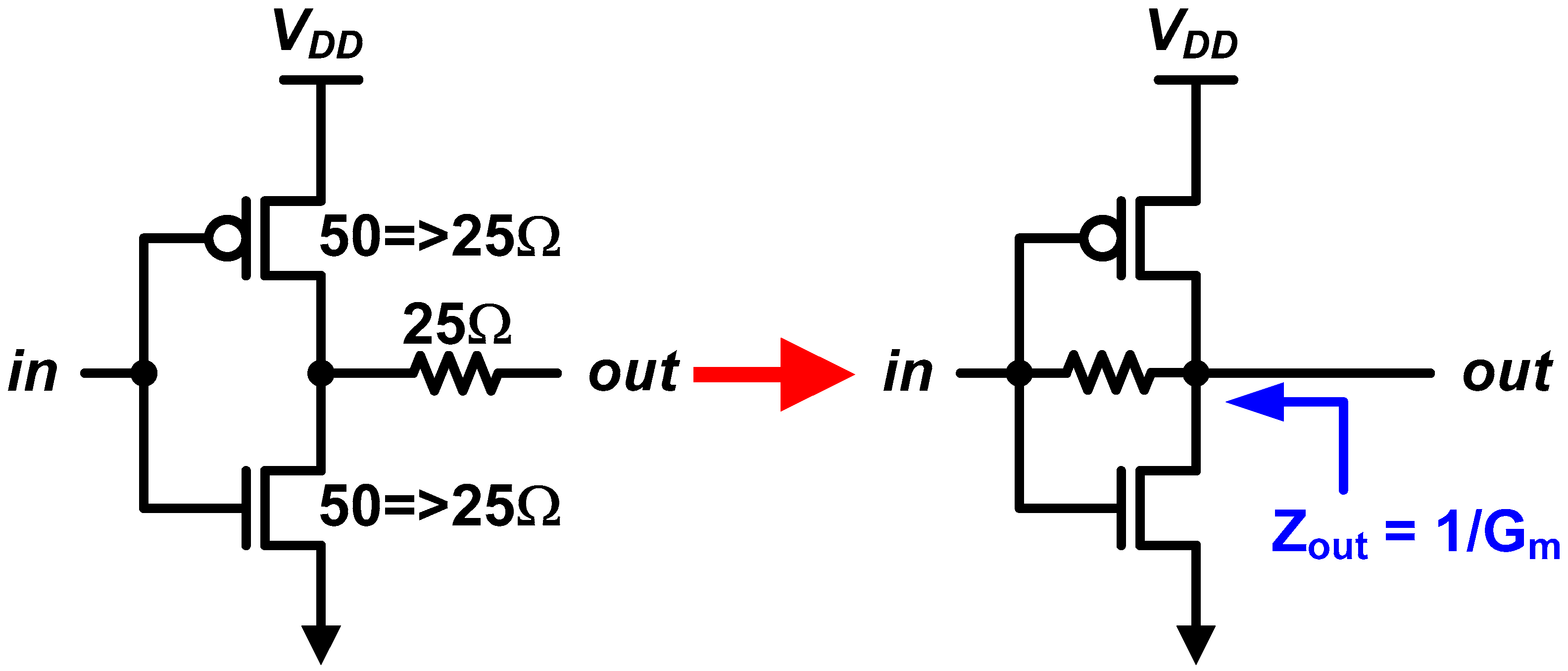
Rather than putting a series resistor, it has been proposed that using a feedback resistor can change the game [13,40,44,50], which is shown in Figure 14. As we studied, the feedback resistor sets the biasing point that the CMOS operates in the saturation region. In addition, the DC output impedance becomes 1/gm, instead of 1/gds. That means we can achieve a high current density of the saturation region and a low output impedance from 1/gm as well. In addition, the gm is easy to be regulated by using a well-known constant-gm bias circuit [13,57].
Although the feedback resistance does not affect the DC output impedance, the high-frequency output impedance, which affects the return loss of the transmitter, is a function of the feedback resistance. The output impedance is calculated as:
where Cin is the input capacitance of the driver [50]. We can find that the feedback introduces both zero (at ) and pole (at ). As a result, the output impedance becomes ro at a very high frequency. Therefore, a designer should carefully choose a proper RF such that guarantees the zero frequency is higher than the Nyquist frequency of the transmit data.
On the other hand, there are two downsides of the resistive-feedback SST driver; low output swing and power consumption. Since the transistor should operate in the deep saturation region to have high ro, the output impedance deviates from 1/gm, which is maintained by the constant-gm biasing, when the output swing increases. It also dissipates a higher current than that of the conventional SST driver due to the short-circuit current. However, as the data rate increases, the pre-driver’s dynamic switching power, which is consumed for driving high input capacitance, dramatically increases. Note that the dynamic power is proportional to the switching frequency and the capacitance, whereas the driver’s current consumption is fixed regardless of the data rate (I = Vswing/100Ω). As a result, it surpasses the static power consumption of the output driver [42]. As a result, the pre-driver power reduction, thanks to the small input capacitance of the resistive-feedback SST driver, is able to fully compensate the increased static power.
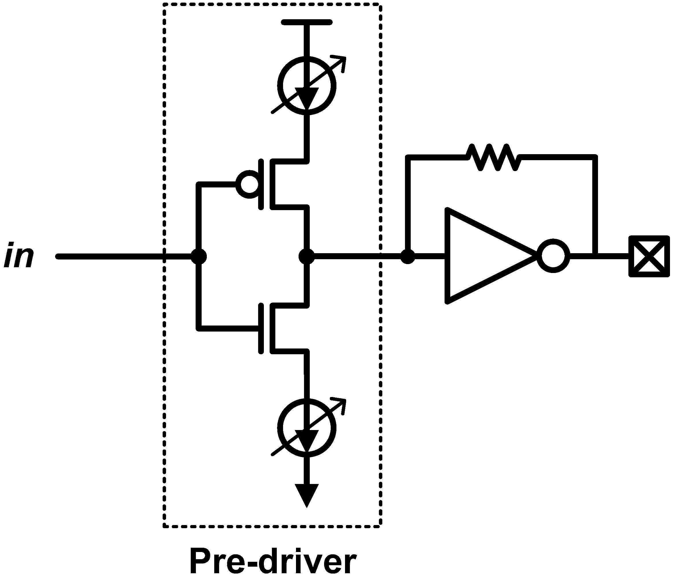
Another advantage of this driver is a simple slicing implementation because of its inherent current-driven nature. In the conventional drivers (including CML and SST), the output driver should be sliced to control the swing and the equalization coefficient; thus, it increases the complexity and the parasitic. On the other hand, in the resistive-feedback SST driver, the slicing can be included in the current-mode pre-driver as shown in Figure 15. That is, a simple current digital-to-analog convertor (DAC) in the pre-driver can replace the slicing at the output stage; thus, it significantly reduces the design complexity and parasitic effects. It has also been proven that the current DAC-based pre-driver is beneficial for pulse-amplitude modulation signaling in [40], where a fabricated 28-Gb/s PAM-4 transmitter chip is presented.
5. Conclusions
This paper introduces three state-of-the-art applications of CMOS inverter with resistor feedback, by providing the basic theories of those applications and the state-of-the-arts implementation results. The focus of this paper is not just enumerating the prior arts, but emphasizing the potential of CMOS inverter as an analog circuit. As discussed in the introduction, CMOS inverter becomes more powerful whereas the conventional analog circuits become less effective as technology scales down. As a result, I believe that there are a lot of undiscovered usages of the CMOS inverter, which will need thorough examination in future research.
Funding
This research received no external funding.
Conflicts of Interest
The authors declare no conflict of interest.
References
- Vertregt, M. The analog challenge of nanometer CMOS. In Proceedings of the 2006 IEEE International Electron Devices Meeting, San Francisco, CA, USA, 11–13 December 2006; pp. 1–8. [Google Scholar]
- Horowitz, M. 1.1 computing’s energy problem (and what we can do about it). In Proceedings of the 2014 IEEE International Solid-State Circuits Conference Digest of Technical Papers (ISSCC), San Francisco, CA, USA, 9–13 February 2014; pp. 10–14. [Google Scholar]
- Babayan-Mashhadi, S.; Lotfi, R. Analysis and design of a low-voltage low-power double-tail comparator. IEEE Trans. VLSI Syst. 2013, 22, 343–352. [Google Scholar] [CrossRef]
- Rajput, S.S.; Jamuar, S.S. Low voltage analog circuit design techniques. IEEE Circuits Syst. Mag. 2002, 2, 24–42. [Google Scholar] [CrossRef]
- Hou, C. 1.1 A smart design paradigm for smart chips. In Proceedings of the 2017 IEEE International Solid-State Circuits Conference (ISSCC), San Frsancisco, CA, USA, 5–9 February 2017; pp. 8–13. [Google Scholar]
- Bae, W.; Jeong, G.S.; Kim, Y.; Chi, H.K.; Jeong, D.K. Design of silicon photonic interconnect ICS in 65-nm CMOS technology. IEEE Trans. VLSI Syst. 2015, 24, 2234–2243. [Google Scholar] [CrossRef]
- Frans, Y.; McLeod, S.; Hedayati, H.; Elzeftawi, M.; Namkoong, J.; Lin, W.; Im, J.; Upadhyaya, P.; Chang, K. A 40-to-64 Gb/s NRZ transmitter with supply-regulated front-end in 16 nm FinFET. IEEE J. Solid-State Circuits 2016, 51, 3167–3177. [Google Scholar] [CrossRef]
- Okuma, Y.; Ishida, K.; Ryu, Y.; Zhang, X.; Chen, P.H.; Watanabe, K.; Sakurai, T. 0.5-V input digital LDO with 98.7% current efficiency and 2.7-µA quiescent current in 65nm CMOS. In Proceedings of the IEEE Custom Integrated Circuits Conference, San Jose, CA, USA, 19–22 September 2010; pp. 1–4. [Google Scholar]
- Chae, Y.; Han, G. Low voltage, low power, inverter-based switched-capacitor delta-sigma modulator. IEEE J. Solid-State Circuits 2009, 44, 458–472. [Google Scholar] [CrossRef]
- Thompson, S.E.; Sun, G.; Choi, Y.S.; Nishida, T. Uniaxial-process-induced strained-Si: Extending the CMOS roadmap. IEEE Trans. Electron Devices 2006, 53, 1010–1020. [Google Scholar] [CrossRef]
- Pidin, S.; Mori, T.; Inoue, K.; Fukuta, S.; Itoh, N.; Mutoh, E.; Saiki, T. A novel strain enhanced CMOS architecture using selectively deposited high tensile and high compressive silicon nitride films. In Proceedings of the IEDM Technical Digest. IEEE International Electron Devices Meeting, San Francisco, CA, USA, 13–15 December 2004; pp. 213–216. [Google Scholar]
- Ghani, T.; Armstrong, M.; Auth, C.; Bost, M.; Charvat, P.; Glass, G.; McIntyre, B. A 90nm high volume manufacturing logic technology featuring novel 45nm gate length strained silicon CMOS transistors. In Proceedings of the IEEE International Electron Devices Meeting, Washington, DC, USA, 8–10 December 2003; pp. 11.6.1–11.6.3. [Google Scholar]
- Jeong, G.S.; Chu, S.H.; Kim, Y.; Jang, S.; Kim, S.; Bae, W.; Jeong, D.K. A 20 Gb/s 0.4 pJ/b Energy-Efficient Transmitter Driver Utilizing Constant-Gm Bias. IEEE J. Solid-State Circuits 2016, 51, 2312–2327. [Google Scholar] [CrossRef]
- Woodward, T.K.; Krishnamoorthy, A.V. 1 Gbit/s CMOS photoreceiver with integrated detector operating at 850 nm. Electron. Lett. 1998, 34, 1252–1253. [Google Scholar] [CrossRef]
- Pan, Q.; Wang, Y.; Yue, C.P. A 42-dBΩ 25-Gb/s CMOS Transimpedance Amplifier with Multiple-Peaking Scheme for Optical Communications. IEEE Transactions on Circuits and Systems II: Express Briefs; IEEE: Piscataway, NJ, USA, 2019. [Google Scholar]
- Martins, M.A.; Mak, P.I.; Martins, R.P. A 0.02-to-6GHz SDR balun-LNA using a triple-stage inverter-based amplifier. In Proceedings of the 2012 IEEE International Symposium on Circuits and Systems, Seoul, North Korea, 20–23 May 2012; pp. 472–475. [Google Scholar]
- Costa, A.L.T.; Klimach, H.; Bampi, S. Ultra-low voltage wideband inductorless balun LNA with high gain and high IP2 for sub-GHz applications. In Proceedings of the 2016 IEEE International Symposium on Circuits and Systems (ISCAS), Montreal, QC, Canada, 22–25 May 2016; pp. 289–292. [Google Scholar]
- Proesel, J.; Schow, C.; Rylyakov, A. 25Gb/s 3.6 pJ/b and 15Gb/s 1.37 pJ/b VCSEL-based optical links in 90 nm CMOS. In Proceedings of the 2012 IEEE International Solid-State Circuits Conference, San Francisco, CA, USA, 19–23 February 2012; pp. 418–420. [Google Scholar]
- Kim, J.; Buckwalter, J.F. A 40-Gb/s optical transceiver front-end in 45 nm SOI CMOS. IEEE J. Solid-State Circuits 2012, 47, 615–626. [Google Scholar] [CrossRef]
- Sun, C.; Georgas, M.; Orcutt, J.; Moss, B.; Chen, Y.H.; Shainline, J.; Miller, D. A monolithically-integrated chip-to-chip optical link in bulk CMOS. IEEE J. Solid-State Circuits 2015, 50, 828–844. [Google Scholar] [CrossRef]
- Chu, S.H.; Bae, W.; Jeong, G.S.; Jang, S.; Kim, S.; Joo, J.; Kim, G.; Jeong, D.K. A 22 to 26.5 Gb/s optical receiver with all-digital clock and data recovery in a 65 nm CMOS process. IEEE J. Solid-State Circuits 2015, 50, 2603–2612. [Google Scholar] [CrossRef]
- Subramaniyan, H.K.; Klumperink, E.A.; Srinivasan, V.; Kiaei, A.; Nauta, B. RF transconductor linearization robust to process, voltage and temperature variations. IEEE J. Solid-State Circuits 2015, 50, 2591–2602. [Google Scholar] [CrossRef]
- Yu, K.; Li, C.; Li, H.; Titriku, A.; Shafik, A.; Wang, B.; Chiang, P.Y. A 25 gb/s hybrid-integrated silicon photonic source-synchronous receiver with microring wavelength stabilization. IEEE J. Solid-State Circuits 2016, 51, 2129–2141. [Google Scholar] [CrossRef]
- Shopov, S.; Voinigescu, S.P. A 3 × 60 Gb/s Transmitter/Repeater Front-End With 4.3 VPP Single-Ended Output Swing in a 28nm UTBB FD-SOI Technology. IEEE J. Solid-State Circuits 2016, 51, 1651–1662. [Google Scholar] [CrossRef]
- Ozkaya, I.; Cevrero, A.; Francese, P.A.; Menolfi, C.; Morf, T.; Brändli, M.; Kossel, M. A 64-Gb/s 1.4-pJ/b NRZ optical receiver data-path in 14-nm CMOS FinFET. IEEE J. Solid-State Circuits 2017, 52, 3458–3473. [Google Scholar] [CrossRef]
- Fard, M.M.P.; Liboiron-Ladouceur, O.; Cowan, G.E. 1.23-pJ/bit 25-Gb/s Inductor-Less Optical Receiver With Low-Voltage Silicon Photodetector. IEEE J. Solid-State Circuits 2018, 53, 1793–1805. [Google Scholar] [CrossRef]
- Hiratsuka, A.; Tsuchiya, A.; Onodera, H. Power-bandwidth trade-off analysis of multi-stage inverter-type transimpedance amplifier for optical communication. In Proceedings of the 2017 IEEE 60th International Midwest Symposium on Circuits and Systems (MWSCAS), Medford, MA, USA, 6–9 August 2017; pp. 795–798. [Google Scholar]
- Jeong, G.S.; Bae, W.; Jeong, D.K. Review of CMOS integrated circuit technologies for high-speed photo-detection. Sensors 2017, 17, 1962. [Google Scholar] [CrossRef]
- Li, H.; Balamurugan, G.; Jaussi, J.; Casper, B. A 112 Gb/s PAM4 Linear TIA with 0.96 pJ/bit Energy Efficiency in 28 nm CMOS. In Proceedings of the ESSCIRC 2018-IEEE 44th European Solid State Circuits Conference (ESSCIRC), Dresden, Germany, 3–6 September 2018; pp. 238–241. [Google Scholar]
- Wang, P.; Ytterdal, T. A 54- μW Inverter-Based Low-Noise Single-Ended to Differential VGA for Second Harmonic Ultrasound Probes in 65-nm CMOS. IEEE Trans. Circuits Syst. I Express Br. 2016, 63, 623–627. [Google Scholar]
- Li, H.; Chen, S.; Yang, L.; Bai, R.; Hu, W.; Zhong, F.Y.; Chiang, P.Y. A 0.8 V, 560fJ/bit, 14Gb/s injection-locked receiver with input duty-cycle distortion tolerable edge-rotating 5/4X sub-rate CDR in 65nm CMOS. In Proceedings of the 2014 Symposium on VLSI Circuits Digest of Technical Papers, Honolulu, HI, USA, 10–13 June 2014; pp. 1–2. [Google Scholar]
- Bae, J.; Kim, J.Y.; Yoo, H.J.A. 0.6 pJ/b 3Gb/s/ch Transceiver in 0.18 μm CMOS for 10mm On-chip Interconnects. In Proceedings of the 2008 IEEE International Symposium on Circuits and Systems, Seattle, WA, USA, 18–21 May 2008; pp. 2861–2864. [Google Scholar]
- Chen, S.; Zhou, L.; Zhuang, I.; Im, J.; Melek, D.; Namkoong, J.; Chang, K. A 4-to-16GHz inverter-based injection-locked quadrature clock generator with phase interpolators for multi-standard I/Os in 7nm FinFET. In Proceedings of the 2018 IEEE International Solid-State Circuits Conference-(ISSCC), San Francisco, CA, USA, 11–15 February 2018; pp. 390–392. [Google Scholar]
- Wang, H.; Lee, J. A 21-Gb/s 87-mW transceiver with FFE/DFE/analog equalizer in 65-nm CMOS technology. IEEE J. Solid-State Circuits 2010, 45, 909–920. [Google Scholar] [CrossRef]
- Song, Y.H.; Bai, R.; Hu, K.; Yang, H.W.; Chiang, P.Y.; Palermo, S. A 0.47–0.66 pJ/bit, 4.8–8 Gb/s I/O transceiver in 65 nm CMOS. IEEE J. Solid-State Circuits 2013, 48, 1276–1289. [Google Scholar] [CrossRef]
- Savoj, J.; Hsieh, K.C.H.; An, F.T.; Gong, J.; Im, J.; Jiang, X.; Turker, D.Z. A low-power 0.5–6.6 Gb/s wireline transceiver embedded in low-cost 28 nm FPGAs. IEEE J. Solid-State Circuits 2013, 48, 2582–2594. [Google Scholar] [CrossRef]
- Menolfi, C.; Toifl, T.; Buchmann, P.; Kossel, M.; Morf, T.; Weiss, J.; Schmatz, M. A 16Gb/s source-series terminated transmitter in 65nm CMOS SOI. In Proceedings of the 2007 IEEE International Solid-State Circuits Conference. Digest of Technical Papers, San Francisco, CA, USA, 11–15 February 2007; pp. 446–614. [Google Scholar]
- Song, Y.H.; Yang, H.W.; Li, H.; Chiang, P.Y.; Palermo, S. An 8–16 Gb/s, 0.65–1.05 pJ/b, voltage-mode transmitter with analog impedance modulation equalization and sub-3 ns power-state transitioning. IEEE J. Solid-State Circuits 2014, 49, 2631–2643. [Google Scholar] [CrossRef]
- Bae, W.; Ju, H.; Park, K.; Cho, S.Y.; Jeong, D.K. A 7.6 mW, 414 fs RMS-jitter 10 GHz phase-locked loop for a 40 Gb/s serial link transmitter based on a two-stage ring oscillator in 65 nm CMOS. IEEE J. Solid-State Circuits 2016, 51, 2357–2367. [Google Scholar] [CrossRef]
- Ju, H.; Choi, M.C.; Jeong, G.S.; Bae, W.; Jeong, D.K. A 28 Gb/s 1.6 pJ/b PAM-4 Transmitter Using Fractionally Spaced 3-Tap FFE and $ G_ {m} $-Regulated Resistive-Feedback Driver. IEEE Trans. Circuits Syst. Ii: Express Br. 2017, 64, 1377–1381. [Google Scholar] [CrossRef]
- Jeong, G.S.; Hwang, J.; Choi, H.S.; Do, H.; Koh, D.; Yun, D.; Joo, J. 25-Gb/s Clocked Pluggable Optics for High-Density Data Center Interconnections. IEEE Trans. Circuits Syst. Ii: Express Br. 2018, 65, 1395–1399. [Google Scholar] [CrossRef]
- Bae, W.; Ju, H.; Park, K.; Han, J.; Jeong, D.K. A supply-scalable-serializing transmitter with controllable output swing and equalization for next-generation standards. IEEE Trans. Ind. Electron. 2018, 65, 5979–5989. [Google Scholar] [CrossRef]
- Bae, W.; Jeong, D.K. A power-efficient 600-mVpp voltage-mode driver with independently matched pull-up and pull-down impedances. Int. J. Circuit Theory Appl. 2015, 43, 2057–2071. [Google Scholar] [CrossRef]
- Ahn, G.; Jeong, D.K.; Kim, G. A 2-Gbaud 0.7-V swing voltage-mode driver and on-chip terminator for high-speed NRZ data transmission. IEEE J. Solid-State Circuits 2000, 35, 915–918. [Google Scholar]
- Fukuda, K.; Yamashita, H.; Ono, G.; Nemoto, R.; Suzuki, E.; Masuda, N.; Saito, T. A 12.3-mW 12.5-Gb/s complete transceiver in 65-nm CMOS process. IEEE J. Solid-State Circuits 2010, 45, 2838–2849. [Google Scholar] [CrossRef]
- Kaviani, K.; Wu, T.; Wei, J.; Amirkhany, A.; Shen, J.; Chin, T.J.; Chuang, B.R. A tri-modal 20-Gbps/link differential/DDR3/GDDR5 memory interface. IEEE J. Solid-State Circuits 2012, 47, 926–937. [Google Scholar] [CrossRef]
- Kaviani, K.; Amirkhany, A.; Huang, C.; Le, P.; Beyene, W.T.; Madden, C.; Yuan, X.C. A 0.4-mW/Gb/s near-ground receiver front-end with replica transconductance termination calibration for a 16-Gb/s source-series terminated transceiver. IEEE J. Solid-State Circuits 2013, 48, 636–648. [Google Scholar] [CrossRef]
- Chan, K.L.; Tan, K.H.; Frans, Y.; Im, J.; Upadhyaya, P.; Lim, S.W.; Chiang, P.C. A 32.75-Gb/s voltage-mode transmitter with three-tap FFE in 16-nm CMOS. IEEE J. Solid-State Circuits 2017, 52, 2663–2678. [Google Scholar] [CrossRef]
- Upadhyaya, P.; Poon, C.F.; Lim, S.W.; Cho, J.; Roldan, A.; Zhang, W.; Zhang, H. A Fully Adaptive 19–58-Gb/s PAM-4 and 9.5–29-Gb/s NRZ Wireline Transceiver with Configurable ADC in 16-nm FinFET. IEEE J. Solid-State Circuits 2018, 54, 18–28. [Google Scholar] [CrossRef]
- Bae, W.; Jeong, G.S.; Jeong, D.K. A 1-pJ/bit, 10-Gb/s/ch forwarded-clock transmitter using a resistive feedback inverter-based driver in 65-nm CMOS. IEEE Trans. Circuits Syst. Express Br. 2016, 63, 1106–1110. [Google Scholar] [CrossRef]
- Park, S.M.; Toumazou, C. A packaged low-noise high-speed regulated cascode transimpedance amplifier using a 0.6 µm N-well CMOS technology. In Proceedings of the 26th European Solid-State Circuits Conference, Stockholm, Sweden, 19–21 September 2000; pp. 431–434. [Google Scholar]
- Kromer, C.; Sialm, G.; Morf, T.; Schmatz, M.L.; Ellinger, F.; Erni, D.; Jackel, H. A low-power 20-GHz 52-dB/spl Omega/transimpedance amplifier in 80-nm CMOS. IEEE J. Solid-State Circuits 2004, 39, 885–894. [Google Scholar] [CrossRef]
- Bae, W.; Nikolić, B.; Jeong, D.K. Use of Phase Delay Analysis for Evaluating Wideband Circuits: An Alternative to Group Delay Analysis. Ieee Trans. VLSI Syst. 2017, 25, 3543–3547. [Google Scholar] [CrossRef]
- Casper, B.; O’Mahony, F. Clocking analysis, implementation and measurement techniques for high-speed data links—A tutorial. IEEE Trans. Circuits Syst. I: Regul. Pap. 2009, 56, 17–39. [Google Scholar] [CrossRef]
- Jeong, D.K.; Borriello, G.; Hodges, D.A.; Katz, R.H. Design of PLL-based clock generation circuits. IEEE J. Solid-State Circuits 1987, 22, 255–261. [Google Scholar] [CrossRef]
- Mansuri, M.; Yang, C.K. A low-power adaptive bandwidth PLL and clock buffer with supply-noise compensation. IEEE J. Solid-State Circuits 2003, 38, 1804–1812. [Google Scholar] [CrossRef]
- Johns, D.A.; Martin, K. Analog Integrated Circuit Design; John Wiley & Sons: Hoboken, NJ, USA, 2008. [Google Scholar]
Figure 1.
Comparison of stacked over non-stacked structure using common-source (CS) amplifier topology. (a) Gain degradation as a function of VDD/VTH [6], (b) large-signal bandwidth degradation as a function of current consumption [7], (c) circuit diagram of a CS amplifier.

Figure 2.
Utilization of gm of PMOS in a CMOS inverter.

Figure 3.
Inverter gain curve and distinction between digital and analog.

Figure 4.
CMOS inverter with resistive feedback.

Figure 5.
Trans-impedance amplifier examples.

Figure 6.
(a) Inverter TIA with series peaking, (b) with inductive feedback.

Figure 7.
Inverter-based multi-stage amplifier with common-mode feedback.

Figure 8.
Magnitude response of CMOS inverter.

Figure 9.
(a) Small signal diagram of resistive feedback inverter, (b) verification of (7).

Figure 10.
(a) AC-coupled resistive feedback inverter and (b) Miller approximation to calculate high-pass cut-off frequency.
Figure 10.
(a) AC-coupled resistive feedback inverter and (b) Miller approximation to calculate high-pass cut-off frequency.

Figure 11.
Duty cycle transfer curve of AC-coupled buffer.

Figure 12.
Conceptual diagram of source-series terminated (SST) driver and practical implementation of N-over-N and P-over-N SST configurations.
Figure 12.
Conceptual diagram of source-series terminated (SST) driver and practical implementation of N-over-N and P-over-N SST configurations.

Figure 13.
SST driver with series resistance.

Figure 14.
Output driver based on resistive-feedback inverter.

Figure 15.
Current-mode pre-driver for resistive-feedback SST driver.

© 2019 by the author. Licensee MDPI, Basel, Switzerland. This article is an open access article distributed under the terms and conditions of the Creative Commons Attribution (CC BY) license (http://creativecommons.org/licenses/by/4.0/).
Share and Cite
MDPI and ACS Style
Bae, W. CMOS Inverter as Analog Circuit: An Overview. J. Low Power Electron. Appl. 2019, 9, 26. https://0-doi-org.brum.beds.ac.uk/10.3390/jlpea9030026
AMA Style
Bae W. CMOS Inverter as Analog Circuit: An Overview. Journal of Low Power Electronics and Applications. 2019; 9(3):26. https://0-doi-org.brum.beds.ac.uk/10.3390/jlpea9030026
Chicago/Turabian StyleBae, Woorham. 2019. "CMOS Inverter as Analog Circuit: An Overview" Journal of Low Power Electronics and Applications 9, no. 3: 26. https://0-doi-org.brum.beds.ac.uk/10.3390/jlpea9030026
Note that from the first issue of 2016, this journal uses article numbers instead of page numbers. See further details here.